JP5148076B2 - 半導体デバイスに格納された電荷の分布を抽出するための方法 - Google Patents
半導体デバイスに格納された電荷の分布を抽出するための方法 Download PDFInfo
- Publication number
- JP5148076B2 JP5148076B2 JP2006154455A JP2006154455A JP5148076B2 JP 5148076 B2 JP5148076 B2 JP 5148076B2 JP 2006154455 A JP2006154455 A JP 2006154455A JP 2006154455 A JP2006154455 A JP 2006154455A JP 5148076 B2 JP5148076 B2 JP 5148076B2
- Authority
- JP
- Japan
- Prior art keywords
- charge
- pulse
- voltage
- curve
- semiconductor device
- Prior art date
- Legal status (The legal status is an assumption and is not a legal conclusion. Google has not performed a legal analysis and makes no representation as to the accuracy of the status listed.)
- Expired - Fee Related
Links
- 238000009826 distribution Methods 0.000 title claims abstract description 80
- 238000000034 method Methods 0.000 title claims abstract description 42
- 239000004065 semiconductor Substances 0.000 title claims abstract description 42
- 238000005086 pumping Methods 0.000 claims abstract description 135
- 230000005527 interface trap Effects 0.000 claims description 35
- 230000008859 change Effects 0.000 claims description 13
- 238000004364 calculation method Methods 0.000 claims description 2
- 230000003247 decreasing effect Effects 0.000 claims description 2
- 239000002800 charge carrier Substances 0.000 claims 2
- 230000000116 mitigating effect Effects 0.000 claims 1
- 238000005259 measurement Methods 0.000 abstract description 46
- 238000012360 testing method Methods 0.000 abstract description 7
- 238000000605 extraction Methods 0.000 description 27
- 239000000758 substrate Substances 0.000 description 13
- 150000004767 nitrides Chemical class 0.000 description 12
- 238000003860 storage Methods 0.000 description 12
- 238000002347 injection Methods 0.000 description 9
- 239000007924 injection Substances 0.000 description 9
- 230000006870 function Effects 0.000 description 8
- 239000000969 carrier Substances 0.000 description 7
- 230000015556 catabolic process Effects 0.000 description 7
- 238000006731 degradation reaction Methods 0.000 description 7
- VYPSYNLAJGMNEJ-UHFFFAOYSA-N Silicium dioxide Chemical compound O=[Si]=O VYPSYNLAJGMNEJ-UHFFFAOYSA-N 0.000 description 6
- 230000009471 action Effects 0.000 description 6
- 229910052814 silicon oxide Inorganic materials 0.000 description 6
- 239000000463 material Substances 0.000 description 5
- 230000007246 mechanism Effects 0.000 description 5
- 229910021420 polycrystalline silicon Inorganic materials 0.000 description 5
- XUIMIQQOPSSXEZ-UHFFFAOYSA-N Silicon Chemical compound [Si] XUIMIQQOPSSXEZ-UHFFFAOYSA-N 0.000 description 4
- 229910052710 silicon Inorganic materials 0.000 description 4
- 239000010703 silicon Substances 0.000 description 4
- 125000006850 spacer group Chemical group 0.000 description 4
- 229910052581 Si3N4 Inorganic materials 0.000 description 3
- 239000003990 capacitor Substances 0.000 description 3
- 230000007423 decrease Effects 0.000 description 3
- 238000005516 engineering process Methods 0.000 description 3
- 230000014759 maintenance of location Effects 0.000 description 3
- 238000001208 nuclear magnetic resonance pulse sequence Methods 0.000 description 3
- 229920005591 polysilicon Polymers 0.000 description 3
- HQVNEWCFYHHQES-UHFFFAOYSA-N silicon nitride Chemical compound N12[Si]34N5[Si]62N3[Si]51N64 HQVNEWCFYHHQES-UHFFFAOYSA-N 0.000 description 3
- 238000009825 accumulation Methods 0.000 description 2
- 239000003989 dielectric material Substances 0.000 description 2
- 238000007667 floating Methods 0.000 description 2
- 230000014509 gene expression Effects 0.000 description 2
- 239000012212 insulator Substances 0.000 description 2
- 238000004519 manufacturing process Methods 0.000 description 2
- 238000000691 measurement method Methods 0.000 description 2
- 238000005457 optimization Methods 0.000 description 2
- 239000002245 particle Substances 0.000 description 2
- 238000012545 processing Methods 0.000 description 2
- 230000003252 repetitive effect Effects 0.000 description 2
- 230000035945 sensitivity Effects 0.000 description 2
- 241001582326 Renia Species 0.000 description 1
- ATJFFYVFTNAWJD-UHFFFAOYSA-N Tin Chemical compound [Sn] ATJFFYVFTNAWJD-UHFFFAOYSA-N 0.000 description 1
- PNEYBMLMFCGWSK-UHFFFAOYSA-N aluminium oxide Inorganic materials [O-2].[O-2].[O-2].[Al+3].[Al+3] PNEYBMLMFCGWSK-UHFFFAOYSA-N 0.000 description 1
- 238000010205 computational analysis Methods 0.000 description 1
- 230000007850 degeneration Effects 0.000 description 1
- 238000011161 development Methods 0.000 description 1
- 230000000694 effects Effects 0.000 description 1
- 230000005684 electric field Effects 0.000 description 1
- 230000005669 field effect Effects 0.000 description 1
- -1 for example Substances 0.000 description 1
- 229910052732 germanium Inorganic materials 0.000 description 1
- GNPVGFCGXDBREM-UHFFFAOYSA-N germanium atom Chemical compound [Ge] GNPVGFCGXDBREM-UHFFFAOYSA-N 0.000 description 1
- 229910000449 hafnium oxide Inorganic materials 0.000 description 1
- WIHZLLGSGQNAGK-UHFFFAOYSA-N hafnium(4+);oxygen(2-) Chemical compound [O-2].[O-2].[Hf+4] WIHZLLGSGQNAGK-UHFFFAOYSA-N 0.000 description 1
- 239000002784 hot electron Substances 0.000 description 1
- 230000006872 improvement Effects 0.000 description 1
- 230000010354 integration Effects 0.000 description 1
- 238000002955 isolation Methods 0.000 description 1
- 229910052751 metal Inorganic materials 0.000 description 1
- 239000002184 metal Substances 0.000 description 1
- 239000002082 metal nanoparticle Substances 0.000 description 1
- 229910044991 metal oxide Inorganic materials 0.000 description 1
- 150000004706 metal oxides Chemical class 0.000 description 1
- 150000002739 metals Chemical class 0.000 description 1
- 239000013081 microcrystal Substances 0.000 description 1
- 238000012986 modification Methods 0.000 description 1
- 230000004048 modification Effects 0.000 description 1
- 239000002159 nanocrystal Substances 0.000 description 1
- 239000003973 paint Substances 0.000 description 1
- 230000008569 process Effects 0.000 description 1
- 230000000750 progressive effect Effects 0.000 description 1
- 230000000717 retained effect Effects 0.000 description 1
- 230000000630 rising effect Effects 0.000 description 1
- 229920006395 saturated elastomer Polymers 0.000 description 1
- HBMJWWWQQXIZIP-UHFFFAOYSA-N silicon carbide Chemical compound [Si+]#[C-] HBMJWWWQQXIZIP-UHFFFAOYSA-N 0.000 description 1
- 229910010271 silicon carbide Inorganic materials 0.000 description 1
- 239000007787 solid Substances 0.000 description 1
- 238000010408 sweeping Methods 0.000 description 1
- 238000012546 transfer Methods 0.000 description 1
- 230000005641 tunneling Effects 0.000 description 1
Images


Classifications
-
- G—PHYSICS
- G11—INFORMATION STORAGE
- G11C—STATIC STORES
- G11C16/00—Erasable programmable read-only memories
- G11C16/02—Erasable programmable read-only memories electrically programmable
- G11C16/04—Erasable programmable read-only memories electrically programmable using variable threshold transistors, e.g. FAMOS
- G11C16/0466—Erasable programmable read-only memories electrically programmable using variable threshold transistors, e.g. FAMOS comprising cells with charge storage in an insulating layer, e.g. metal-nitride-oxide-silicon [MNOS], silicon-oxide-nitride-oxide-silicon [SONOS]
- G11C16/0475—Erasable programmable read-only memories electrically programmable using variable threshold transistors, e.g. FAMOS comprising cells with charge storage in an insulating layer, e.g. metal-nitride-oxide-silicon [MNOS], silicon-oxide-nitride-oxide-silicon [SONOS] comprising two or more independent storage sites which store independent data
-
- G—PHYSICS
- G11—INFORMATION STORAGE
- G11C—STATIC STORES
- G11C16/00—Erasable programmable read-only memories
- G11C16/02—Erasable programmable read-only memories electrically programmable
- G11C16/06—Auxiliary circuits, e.g. for writing into memory
- G11C16/26—Sensing or reading circuits; Data output circuits
-
- G—PHYSICS
- G11—INFORMATION STORAGE
- G11C—STATIC STORES
- G11C16/00—Erasable programmable read-only memories
- G11C16/02—Erasable programmable read-only memories electrically programmable
- G11C16/06—Auxiliary circuits, e.g. for writing into memory
- G11C16/34—Determination of programming status, e.g. threshold voltage, overprogramming or underprogramming, retention
- G11C16/349—Arrangements for evaluating degradation, retention or wearout, e.g. by counting erase cycles
- G11C16/3495—Circuits or methods to detect or delay wearout of nonvolatile EPROM or EEPROM memory devices, e.g. by counting numbers of erase or reprogram cycles, by using multiple memory areas serially or cyclically
Landscapes
- Engineering & Computer Science (AREA)
- Microelectronics & Electronic Packaging (AREA)
- Semiconductor Memories (AREA)
- Non-Volatile Memory (AREA)
- Testing Of Individual Semiconductor Devices (AREA)
- Read Only Memory (AREA)
- Die Bonding (AREA)
- Semiconductor Integrated Circuits (AREA)
- Electronic Switches (AREA)
- Crystals, And After-Treatments Of Crystals (AREA)
Description

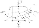
2 基板
3 ゲート電極
4 ゲート誘電体
5 スペーサ
6 ソース
7 ドレイン
8 チャンネル領域
9 別の層
10 電荷トラッピング層
11 別の誘電体の層
Claims (4)
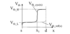
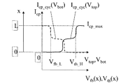
- 有効長Leffを持つ電荷トラッピング層(4)の下方にあるチャンネル(8)および、電荷トラッピング層(4)の上方で、チャンネル層(8)の反対側に配置されたゲート電極(3)を持つ半導体デバイスの電荷トラッピング層(10)に格納された電荷の空間的な分布(Nnt)を抽出するための方法であって、
a)半導体デバイス(1)をプログラミング動作に供し、電荷トラッピング層(10)内でチャンネル長(8)に沿って電荷が単調に増加し、その結果、チャンネル長(8)に沿って単調に変化するしきい値プロフィールVth(x)とすることにより、半導体デバイス(1)を基準状態にするステップと、
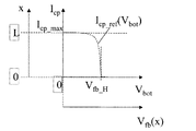
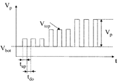
b)前記基準状態にある前記半導体デバイスについて、電圧パルス列を前記ゲート電極に印加して、電圧(Vbot)の関数として電荷ポンピング電流Icp(Vbot)を測定することによって、第1電荷ポンピングカーブを決定し、この場合、このパルス列での各パルスが同じトップレベル電圧を有し、パルスのベースレベル電圧を低下させることによって、パルスの振幅は時間とともに単調に増加するようにし、そして、電圧パルス列を前記ゲート電極に印加して、電圧(Vtop)の関数として電荷ポンピング電流Icp(Vtop)を測定することによって、第2電荷ポンピングカーブを決定し、この場合、このパルス列での各パルスが同じベースレベル電圧を有し、パルスのトップレベル電圧を上昇させることによって、パルスの振幅は時間とともに単調に増加するようにしたステップと、
c)前記半導体デバイスを動作させるステップと、
d)前記動作中の半導体デバイスについて、電圧パルス列を前記ゲート電極に印加して、電圧(Vbot)の関数として電荷ポンピング電流Icp(Vbot)を測定することによって、第1電荷ポンピングカーブを決定し、この場合、このパルス列での各パルスが同じトップレベル電圧を有し、パルスのベースレベル電圧を低下させることによって、パルスの振幅は時間とともに単調に増加するようにし、そして、電圧パルス列を前記ゲート電極に印加して、電圧(Vtop)の関数として電荷ポンピング電流Icp(Vtop)を測定することによって、第2電荷ポンピングカーブを決定し、この場合、このパルス列での各パルスが同じベースレベル電圧を有し、パルスのトップレベル電圧を上昇させることによって、パルスの振幅は時間とともに単調に増加するようにしたステップと、
e)前記決定した電荷ポンピングカーブからのデータを結合して、前記空間的な分布を取得するステップと、を含み、
ステップe)は、
r)開始値および電荷ポンピング電流Icpの範囲を選択し、電荷ポンピング電流Icpの前記選択した値について全ての前記決定した電荷ポンピングカーブにおいて、対応するデータポイントを決定するステップと、
s)電荷ポンピング電流Icpの前記開始値および前記範囲から、前記対応したデータポイントを用いて、下記の数式
ここで、Vth_fer(x)は、基準デバイスのしきい値電圧カーブ、
Vfb_ref(X)は、基準デバイスのフラットバンド電圧カーブ、
Vth_cyc(x)は、少なくとも1つのプログラム/消去動作後の半導体デバイスのしきい値電圧カーブ、
Vfb_cyc(x)は、少なくとも1つのプログラム/消去動作後の半導体デバイスのフラットバンド電圧カーブ、
qは、電子電荷の絶対値、
Nit(x)は、インターフェーストラップ数(個/cm 2 )、
Nnt(x)は、電荷トラッピング層(10)に存在する荷電キャリア数(個/cm 2 )、
fは、変化するレベルの電圧信号の周波数、
Qntは、電荷トラッピング層(10)に存在する電荷(C/cm 2 )、
Qitは、インターフェーストラップに存在する電荷(C/cm 2 )、
xは、半導体デバイスのチャンネルに沿った座標、
Cは、誘電体スタック(4)のキャパシタンス(F/cm 2 )であり、
さらに、t)その後、取得したチャンネル長Lcalcが、前記半導体デバイスの前記有効チャンネル長Leffと実質的に等しいか否かを比較するステップと、
u)等しくなければ、ステップr)〜t)を繰り返すステップと、を含む方法。 - 前記電荷ポンピングカーブからの前記データはさらに結合されて、チャンネル(8)と、電荷トラッピング層(10)をチャンネル層(8)から分離する誘電体スタック(11)との間のインターフェースに存在するトラップ内の電荷空間分布(Nit)を得ることを特徴とする請求項1記載の方法。
- 前記計算で得たチャンネル長Lcalcと、前記有効長Leffとの差が1%未満である請求項1または2記載の方法。
- 電荷ポンピングカーブからトラップ内の前記電荷空間分布(Nit)を得ることは、
y)電荷ポンピングカーブの1つにおいて、開始ポイントを選択するステップと、
z)電荷ポンピングカーブの選択された部分についての開始ポイントから下記の数式
aa)下記の数式
ここで、Vth_fer(x)は、基準デバイスのしきい値電圧カーブ、
Vfb_ref(X)は、基準デバイスのフラットバンド電圧カーブ、
Vth_cyc(x)は、少なくとも1つのプログラム/消去動作後の半導体デバイスのしきい値電圧カーブ、
Vfb_cyc(x)は、少なくとも1つのプログラム/消去動作後の半導体デバイスのフラットバンド電圧カーブ、
qは、電子電荷の絶対値、
ΔNit(x)は、インターフェーストラップ数(個/cm2)、
ΔNnt(x)は、電荷トラッピング層(10)に存在する荷電キャリア数(個/cm2)、
fは、変化するレベルの電圧信号の周波数、
Qntは、電荷トラッピング層(10)に存在する電荷(C/cm2)、
Qitは、インターフェーストラップに存在する電荷(C/cm2)、
xは、半導体デバイスのチャンネルに沿った座標、
Cは、誘電体スタック(4)のキャパシタンス(F/cm2)である、請求項2記載の方法。
Applications Claiming Priority (6)
| Application Number | Priority Date | Filing Date | Title |
|---|---|---|---|
| US68707605P | 2005-06-03 | 2005-06-03 | |
| US60/687,076 | 2005-06-03 | ||
| US70485905P | 2005-08-01 | 2005-08-01 | |
| US60/704,859 | 2005-08-01 | ||
| EP05109600A EP1732080B1 (en) | 2005-06-03 | 2005-10-14 | Method for extracting the distribution of charge stored in a semiconductor device |
| EP05109600.6 | 2005-10-14 |
Publications (2)
| Publication Number | Publication Date |
|---|---|
| JP2006352111A JP2006352111A (ja) | 2006-12-28 |
| JP5148076B2 true JP5148076B2 (ja) | 2013-02-20 |
Family
ID=36975251
Family Applications (2)
| Application Number | Title | Priority Date | Filing Date |
|---|---|---|---|
| JP2006154455A Expired - Fee Related JP5148076B2 (ja) | 2005-06-03 | 2006-06-02 | 半導体デバイスに格納された電荷の分布を抽出するための方法 |
| JP2008514128A Expired - Fee Related JP5191382B2 (ja) | 2005-06-03 | 2006-06-06 | 半導体デバイスに蓄積される電荷の分布の抽出方法 |
Family Applications After (1)
| Application Number | Title | Priority Date | Filing Date |
|---|---|---|---|
| JP2008514128A Expired - Fee Related JP5191382B2 (ja) | 2005-06-03 | 2006-06-06 | 半導体デバイスに蓄積される電荷の分布の抽出方法 |
Country Status (6)
| Country | Link |
|---|---|
| US (2) | US7388785B2 (ja) |
| EP (2) | EP1732080B1 (ja) |
| JP (2) | JP5148076B2 (ja) |
| AT (2) | ATE409350T1 (ja) |
| DE (2) | DE602005009937D1 (ja) |
| WO (1) | WO2006128922A1 (ja) |
Families Citing this family (11)
| Publication number | Priority date | Publication date | Assignee | Title |
|---|---|---|---|---|
| ATE460735T1 (de) * | 2005-06-03 | 2010-03-15 | Imec | Verfahren zur steuerung einen nichtflüchtigen ladungshaftstellen-speicheranordnungen und verfahren zur bestimmung der programmier- /löschparameter |
| JP2007073969A (ja) * | 2005-09-07 | 2007-03-22 | Samsung Electronics Co Ltd | 電荷トラップ型メモリ素子及びその製造方法 |
| US8394683B2 (en) * | 2008-01-15 | 2013-03-12 | Micron Technology, Inc. | Methods of forming semiconductor constructions, and methods of forming NAND unit cells |
| US8841682B2 (en) * | 2009-08-27 | 2014-09-23 | Cree, Inc. | Transistors with a gate insulation layer having a channel depleting interfacial charge and related fabrication methods |
| US8941171B2 (en) * | 2010-07-02 | 2015-01-27 | Micron Technology, Inc. | Flatband voltage adjustment in a semiconductor device |
| JP5801049B2 (ja) * | 2010-12-28 | 2015-10-28 | ラピスセミコンダクタ株式会社 | 半導体記憶装置へのデータの書込み方法及び半導体記憶装置 |
| CN102163568B (zh) * | 2011-03-07 | 2012-10-10 | 北京大学 | 一种提取mos管沿沟道电荷分布的方法 |
| US8832619B2 (en) * | 2013-01-28 | 2014-09-09 | Taiwan Semiconductor Manufacturing Co., Ltd. | Analytical model for predicting current mismatch in metal oxide semiconductor arrays |
| KR102606738B1 (ko) * | 2017-02-10 | 2023-11-24 | 글로벌웨이퍼스 씨오., 엘티디. | 반도체 구조들을 평가하기 위한 방법들 |
| KR102783321B1 (ko) | 2020-08-25 | 2025-03-20 | 삼성디스플레이 주식회사 | 표시 장치 및 이의 구동 방법 |
| CN121389677B (zh) * | 2025-12-26 | 2026-03-24 | 兰州理工大学 | 基于隧穿效应与空穴抽出受限的空间电荷分布计算方法 |
Family Cites Families (16)
| Publication number | Priority date | Publication date | Assignee | Title |
|---|---|---|---|---|
| US5583810A (en) | 1991-01-31 | 1996-12-10 | Interuniversitair Micro-Elektronica Centrum Vzw | Method for programming a semiconductor memory device |
| JP3247396B2 (ja) * | 1991-03-29 | 2002-01-15 | 株式会社東芝 | 半導体装置の評価方法 |
| IL125604A (en) * | 1997-07-30 | 2004-03-28 | Saifun Semiconductors Ltd | Non-volatile electrically erasable and programmble semiconductor memory cell utilizing asymmetrical charge |
| US6768165B1 (en) | 1997-08-01 | 2004-07-27 | Saifun Semiconductors Ltd. | Two bit non-volatile electrically erasable and programmable semiconductor memory cell utilizing asymmetrical charge trapping |
| US6331953B1 (en) * | 2000-02-16 | 2001-12-18 | Advanced Micro Devices | Intelligent ramped gate and ramped drain erasure for non-volatile memory cells |
| US6928001B2 (en) | 2000-12-07 | 2005-08-09 | Saifun Semiconductors Ltd. | Programming and erasing methods for a non-volatile memory cell |
| US6490204B2 (en) * | 2000-05-04 | 2002-12-03 | Saifun Semiconductors Ltd. | Programming and erasing methods for a reference cell of an NROM array |
| US6396741B1 (en) | 2000-05-04 | 2002-05-28 | Saifun Semiconductors Ltd. | Programming of nonvolatile memory cells |
| US6801453B2 (en) * | 2002-04-02 | 2004-10-05 | Macronix International Co., Ltd. | Method and apparatus of a read scheme for non-volatile memory |
| KR100542701B1 (ko) | 2003-11-18 | 2006-01-11 | 주식회사 하이닉스반도체 | 낸드 플래시 메모리 소자의 문턱전압 측정 방법 |
| US7151692B2 (en) * | 2004-01-27 | 2006-12-19 | Macronix International Co., Ltd. | Operation scheme for programming charge trapping non-volatile memory |
| US7075828B2 (en) | 2004-04-26 | 2006-07-11 | Macronix International Co., Intl. | Operation scheme with charge balancing erase for charge trapping non-volatile memory |
| US7345920B2 (en) | 2004-09-09 | 2008-03-18 | Macronix International Co., Ltd. | Method and apparatus for sensing in charge trapping non-volatile memory |
| US20060113586A1 (en) * | 2004-11-29 | 2006-06-01 | Macronix International Co., Ltd. | Charge trapping dielectric structure for non-volatile memory |
| JP2006196650A (ja) * | 2005-01-13 | 2006-07-27 | Sharp Corp | 半導体不揮発性メモリ装置およびその消去方法 |
| ATE460735T1 (de) | 2005-06-03 | 2010-03-15 | Imec | Verfahren zur steuerung einen nichtflüchtigen ladungshaftstellen-speicheranordnungen und verfahren zur bestimmung der programmier- /löschparameter |
-
2005
- 2005-10-14 DE DE602005009937T patent/DE602005009937D1/de not_active Expired - Lifetime
- 2005-10-14 EP EP05109600A patent/EP1732080B1/en not_active Expired - Lifetime
- 2005-10-14 AT AT05109600T patent/ATE409350T1/de not_active IP Right Cessation
-
2006
- 2006-06-02 JP JP2006154455A patent/JP5148076B2/ja not_active Expired - Fee Related
- 2006-06-02 US US11/445,551 patent/US7388785B2/en active Active
- 2006-06-06 AT AT06763541T patent/ATE445901T1/de not_active IP Right Cessation
- 2006-06-06 JP JP2008514128A patent/JP5191382B2/ja not_active Expired - Fee Related
- 2006-06-06 WO PCT/EP2006/062944 patent/WO2006128922A1/en not_active Ceased
- 2006-06-06 EP EP06763541A patent/EP1886320B1/en not_active Not-in-force
- 2006-06-06 DE DE602006009797T patent/DE602006009797D1/de active Active
- 2006-06-06 US US11/916,796 patent/US7933153B2/en not_active Expired - Fee Related
Also Published As
| Publication number | Publication date |
|---|---|
| EP1886320A1 (en) | 2008-02-13 |
| US20060284082A1 (en) | 2006-12-21 |
| EP1886320B1 (en) | 2009-10-14 |
| ATE445901T1 (de) | 2009-10-15 |
| US7933153B2 (en) | 2011-04-26 |
| WO2006128922A1 (en) | 2006-12-07 |
| JP5191382B2 (ja) | 2013-05-08 |
| DE602005009937D1 (de) | 2008-11-06 |
| JP2008546194A (ja) | 2008-12-18 |
| EP1732080B1 (en) | 2008-09-24 |
| ATE409350T1 (de) | 2008-10-15 |
| US7388785B2 (en) | 2008-06-17 |
| EP1732080A1 (en) | 2006-12-13 |
| JP2006352111A (ja) | 2006-12-28 |
| US20090135652A1 (en) | 2009-05-28 |
| DE602006009797D1 (de) | 2009-11-26 |
Similar Documents
| Publication | Publication Date | Title |
|---|---|---|
| US20090141563A1 (en) | Method for Operating a Non-Volatile Charge-Trapping Memory Device and Method for Determining Programming/Erase Conditions | |
| US7688626B2 (en) | Depletion mode bandgap engineered memory | |
| US7642585B2 (en) | Non-volatile memory cells, memory arrays including the same and methods of operating cells and arrays | |
| JP4800683B2 (ja) | 一列の電荷トラッピングメモリセルを作動させるための方法および装置 | |
| US7483307B2 (en) | Method and apparatus for sensing in charge trapping non-volatile memory | |
| JP5148076B2 (ja) | 半導体デバイスに格納された電荷の分布を抽出するための方法 | |
| CN100539161C (zh) | 具有未掺杂源极与汲极区的陷入储存快闪记忆胞结构 | |
| US7072219B1 (en) | Method and apparatus for operating a non-volatile memory array | |
| JP4414126B2 (ja) | 不揮発性メモリ装置の消去方法。 | |
| CN101833993B (zh) | 扩大存储单元操作区间的方法及应用其的非挥发存储器阵列 | |
| US9852801B1 (en) | Method for determining a leakage current through an inter-gate dielectric structure of a flash memory cell | |
| US7130215B2 (en) | Method and apparatus for operating a non-volatile memory device | |
| US20080158966A1 (en) | Variable Program and Program Verification Methods for a Virtual Ground Memory in Easing Buried Drain Contacts | |
| JP2009238858A (ja) | 半導体装置の荷電中心位置の評価方法、半導体装置の荷電中心位置の評価装置、及び半導体装置の荷電中心位置の評価プログラム | |
| CN103761989B (zh) | 利用单电荷技术测量sonos存储器中局域电荷分布的方法 | |
| US7072220B1 (en) | Method and apparatus for operating a non-volatile memory array | |
| US7327611B2 (en) | Method and apparatus for operating charge trapping nonvolatile memory |
Legal Events
| Date | Code | Title | Description |
|---|---|---|---|
| A621 | Written request for application examination |
Free format text: JAPANESE INTERMEDIATE CODE: A621 Effective date: 20090508 |
|
| A977 | Report on retrieval |
Free format text: JAPANESE INTERMEDIATE CODE: A971007 Effective date: 20120315 |
|
| A131 | Notification of reasons for refusal |
Free format text: JAPANESE INTERMEDIATE CODE: A131 Effective date: 20120403 |
|
| A601 | Written request for extension of time |
Free format text: JAPANESE INTERMEDIATE CODE: A601 Effective date: 20120629 |
|
| A602 | Written permission of extension of time |
Free format text: JAPANESE INTERMEDIATE CODE: A602 Effective date: 20120704 |
|
| A601 | Written request for extension of time |
Free format text: JAPANESE INTERMEDIATE CODE: A601 Effective date: 20120801 |
|
| A602 | Written permission of extension of time |
Free format text: JAPANESE INTERMEDIATE CODE: A602 Effective date: 20120806 |
|
| A601 | Written request for extension of time |
Free format text: JAPANESE INTERMEDIATE CODE: A601 Effective date: 20120903 |
|
| A602 | Written permission of extension of time |
Free format text: JAPANESE INTERMEDIATE CODE: A602 Effective date: 20120906 |
|
| A521 | Request for written amendment filed |
Free format text: JAPANESE INTERMEDIATE CODE: A523 Effective date: 20121002 |
|
| TRDD | Decision of grant or rejection written | ||
| A01 | Written decision to grant a patent or to grant a registration (utility model) |
Free format text: JAPANESE INTERMEDIATE CODE: A01 Effective date: 20121030 |
|
| A61 | First payment of annual fees (during grant procedure) |
Free format text: JAPANESE INTERMEDIATE CODE: A61 Effective date: 20121128 |
|
| R150 | Certificate of patent or registration of utility model |
Ref document number: 5148076 Country of ref document: JP Free format text: JAPANESE INTERMEDIATE CODE: R150 Free format text: JAPANESE INTERMEDIATE CODE: R150 |
|
| FPAY | Renewal fee payment (event date is renewal date of database) |
Free format text: PAYMENT UNTIL: 20151207 Year of fee payment: 3 |
|
| R250 | Receipt of annual fees |
Free format text: JAPANESE INTERMEDIATE CODE: R250 |
|
| R250 | Receipt of annual fees |
Free format text: JAPANESE INTERMEDIATE CODE: R250 |
|
| R250 | Receipt of annual fees |
Free format text: JAPANESE INTERMEDIATE CODE: R250 |
|
| R250 | Receipt of annual fees |
Free format text: JAPANESE INTERMEDIATE CODE: R250 |
|
| R250 | Receipt of annual fees |
Free format text: JAPANESE INTERMEDIATE CODE: R250 |
|
| R250 | Receipt of annual fees |
Free format text: JAPANESE INTERMEDIATE CODE: R250 |
|
| LAPS | Cancellation because of no payment of annual fees |