JP5224014B2 - イオンビームに対して汚染粒子を除去するためのシステム及び方法 - Google Patents
イオンビームに対して汚染粒子を除去するためのシステム及び方法 Download PDFInfo
- Publication number
- JP5224014B2 JP5224014B2 JP2002524184A JP2002524184A JP5224014B2 JP 5224014 B2 JP5224014 B2 JP 5224014B2 JP 2002524184 A JP2002524184 A JP 2002524184A JP 2002524184 A JP2002524184 A JP 2002524184A JP 5224014 B2 JP5224014 B2 JP 5224014B2
- Authority
- JP
- Japan
- Prior art keywords
- ion beam
- particles
- electric field
- ion
- ions
- Prior art date
- Legal status (The legal status is an assumption and is not a legal conclusion. Google has not performed a legal analysis and makes no representation as to the accuracy of the status listed.)
- Expired - Lifetime
Links
- 239000002245 particle Substances 0.000 title claims description 174
- 238000010884 ion-beam technique Methods 0.000 title claims description 149
- 238000000034 method Methods 0.000 title claims description 18
- 239000000356 contaminant Substances 0.000 title description 24
- 150000002500 ions Chemical class 0.000 claims description 88
- 230000005684 electric field Effects 0.000 claims description 66
- 238000005468 ion implantation Methods 0.000 claims description 21
- 239000000758 substrate Substances 0.000 claims description 12
- 238000012545 processing Methods 0.000 claims description 10
- 238000002513 implantation Methods 0.000 claims description 9
- 230000002401 inhibitory effect Effects 0.000 claims description 7
- 238000011109 contamination Methods 0.000 claims description 6
- 238000012546 transfer Methods 0.000 claims description 6
- 230000008569 process Effects 0.000 claims description 4
- 238000011144 upstream manufacturing Methods 0.000 claims description 3
- 235000012431 wafers Nutrition 0.000 description 22
- 239000000463 material Substances 0.000 description 16
- 239000004065 semiconductor Substances 0.000 description 12
- 238000004458 analytical method Methods 0.000 description 10
- 230000001133 acceleration Effects 0.000 description 5
- 238000010586 diagram Methods 0.000 description 5
- 230000006870 function Effects 0.000 description 5
- 238000004519 manufacturing process Methods 0.000 description 5
- 238000000354 decomposition reaction Methods 0.000 description 4
- 238000000605 extraction Methods 0.000 description 3
- 239000012535 impurity Substances 0.000 description 3
- 238000006386 neutralization reaction Methods 0.000 description 3
- 229920002120 photoresistant polymer Polymers 0.000 description 3
- 229910052782 aluminium Inorganic materials 0.000 description 2
- XAGFODPZIPBFFR-UHFFFAOYSA-N aluminium Chemical compound [Al] XAGFODPZIPBFFR-UHFFFAOYSA-N 0.000 description 2
- 230000003116 impacting effect Effects 0.000 description 2
- ZOXJGFHDIHLPTG-UHFFFAOYSA-N Boron Chemical compound [B] ZOXJGFHDIHLPTG-UHFFFAOYSA-N 0.000 description 1
- GYHNNYVSQQEPJS-UHFFFAOYSA-N Gallium Chemical compound [Ga] GYHNNYVSQQEPJS-UHFFFAOYSA-N 0.000 description 1
- OAICVXFJPJFONN-UHFFFAOYSA-N Phosphorus Chemical compound [P] OAICVXFJPJFONN-UHFFFAOYSA-N 0.000 description 1
- XUIMIQQOPSSXEZ-UHFFFAOYSA-N Silicon Chemical compound [Si] XUIMIQQOPSSXEZ-UHFFFAOYSA-N 0.000 description 1
- 230000009471 action Effects 0.000 description 1
- 229910052787 antimony Inorganic materials 0.000 description 1
- WATWJIUSRGPENY-UHFFFAOYSA-N antimony atom Chemical compound [Sb] WATWJIUSRGPENY-UHFFFAOYSA-N 0.000 description 1
- 229910052785 arsenic Inorganic materials 0.000 description 1
- RQNWIZPPADIBDY-UHFFFAOYSA-N arsenic atom Chemical compound [As] RQNWIZPPADIBDY-UHFFFAOYSA-N 0.000 description 1
- 230000000712 assembly Effects 0.000 description 1
- 238000000429 assembly Methods 0.000 description 1
- 230000004888 barrier function Effects 0.000 description 1
- 230000008901 benefit Effects 0.000 description 1
- 239000008280 blood Substances 0.000 description 1
- 210000004369 blood Anatomy 0.000 description 1
- 229910052796 boron Inorganic materials 0.000 description 1
- 230000008859 change Effects 0.000 description 1
- 239000011248 coating agent Substances 0.000 description 1
- 238000000576 coating method Methods 0.000 description 1
- 238000004891 communication Methods 0.000 description 1
- 238000010276 construction Methods 0.000 description 1
- 239000013078 crystal Substances 0.000 description 1
- 239000002019 doping agent Substances 0.000 description 1
- 230000009977 dual effect Effects 0.000 description 1
- 239000012777 electrically insulating material Substances 0.000 description 1
- 238000005516 engineering process Methods 0.000 description 1
- 239000012530 fluid Substances 0.000 description 1
- 239000003574 free electron Substances 0.000 description 1
- 229910052733 gallium Inorganic materials 0.000 description 1
- 239000011521 glass Substances 0.000 description 1
- 239000007943 implant Substances 0.000 description 1
- 229910052738 indium Inorganic materials 0.000 description 1
- APFVFJFRJDLVQX-UHFFFAOYSA-N indium atom Chemical compound [In] APFVFJFRJDLVQX-UHFFFAOYSA-N 0.000 description 1
- 238000004949 mass spectrometry Methods 0.000 description 1
- 230000007246 mechanism Effects 0.000 description 1
- 230000005012 migration Effects 0.000 description 1
- 238000013508 migration Methods 0.000 description 1
- 238000012986 modification Methods 0.000 description 1
- 230000004048 modification Effects 0.000 description 1
- 229910052698 phosphorus Inorganic materials 0.000 description 1
- 239000011574 phosphorus Substances 0.000 description 1
- 230000001902 propagating effect Effects 0.000 description 1
- 230000004044 response Effects 0.000 description 1
- 238000007493 shaping process Methods 0.000 description 1
- 229910052710 silicon Inorganic materials 0.000 description 1
- 239000010703 silicon Substances 0.000 description 1
- 125000006850 spacer group Chemical group 0.000 description 1
- 229910001220 stainless steel Inorganic materials 0.000 description 1
- 239000010935 stainless steel Substances 0.000 description 1
- WFKWXMTUELFFGS-UHFFFAOYSA-N tungsten Chemical compound [W] WFKWXMTUELFFGS-UHFFFAOYSA-N 0.000 description 1
- 229910052721 tungsten Inorganic materials 0.000 description 1
- 239000010937 tungsten Substances 0.000 description 1
- 239000011364 vaporized material Substances 0.000 description 1
- 238000004804 winding Methods 0.000 description 1
Images



Classifications
-
- H—ELECTRICITY
- H01—ELECTRIC ELEMENTS
- H01J—ELECTRIC DISCHARGE TUBES OR DISCHARGE LAMPS
- H01J37/00—Discharge tubes with provision for introducing objects or material to be exposed to the discharge, e.g. for the purpose of examination or processing thereof
- H01J37/30—Electron-beam or ion-beam tubes for localised treatment of objects
-
- H—ELECTRICITY
- H01—ELECTRIC ELEMENTS
- H01J—ELECTRIC DISCHARGE TUBES OR DISCHARGE LAMPS
- H01J37/00—Discharge tubes with provision for introducing objects or material to be exposed to the discharge, e.g. for the purpose of examination or processing thereof
- H01J37/02—Details
- H01J37/026—Means for avoiding or neutralising unwanted electrical charges on tube components
-
- H—ELECTRICITY
- H01—ELECTRIC ELEMENTS
- H01J—ELECTRIC DISCHARGE TUBES OR DISCHARGE LAMPS
- H01J37/00—Discharge tubes with provision for introducing objects or material to be exposed to the discharge, e.g. for the purpose of examination or processing thereof
- H01J37/30—Electron-beam or ion-beam tubes for localised treatment of objects
- H01J37/3002—Details
-
- H—ELECTRICITY
- H01—ELECTRIC ELEMENTS
- H01J—ELECTRIC DISCHARGE TUBES OR DISCHARGE LAMPS
- H01J37/00—Discharge tubes with provision for introducing objects or material to be exposed to the discharge, e.g. for the purpose of examination or processing thereof
- H01J37/30—Electron-beam or ion-beam tubes for localised treatment of objects
- H01J37/317—Electron-beam or ion-beam tubes for localised treatment of objects for changing properties of the objects or for applying thin layers thereon, e.g. for ion implantation
- H01J37/3171—Electron-beam or ion-beam tubes for localised treatment of objects for changing properties of the objects or for applying thin layers thereon, e.g. for ion implantation for ion implantation
-
- H—ELECTRICITY
- H01—ELECTRIC ELEMENTS
- H01J—ELECTRIC DISCHARGE TUBES OR DISCHARGE LAMPS
- H01J2237/00—Discharge tubes exposing object to beam, e.g. for analysis treatment, etching, imaging
- H01J2237/004—Charge control of objects or beams
-
- H—ELECTRICITY
- H01—ELECTRIC ELEMENTS
- H01J—ELECTRIC DISCHARGE TUBES OR DISCHARGE LAMPS
- H01J2237/00—Discharge tubes exposing object to beam, e.g. for analysis treatment, etching, imaging
- H01J2237/02—Details
- H01J2237/022—Avoiding or removing foreign or contaminating particles, debris or deposits on sample or tube
-
- H—ELECTRICITY
- H01—ELECTRIC ELEMENTS
- H01J—ELECTRIC DISCHARGE TUBES OR DISCHARGE LAMPS
- H01J2237/00—Discharge tubes exposing object to beam, e.g. for analysis treatment, etching, imaging
- H01J2237/30—Electron or ion beam tubes for processing objects
- H01J2237/317—Processing objects on a microscale
- H01J2237/31701—Ion implantation
- H01J2237/31705—Impurity or contaminant control
Landscapes
- Chemical & Material Sciences (AREA)
- Analytical Chemistry (AREA)
- Physical Vapour Deposition (AREA)
- Plasma Technology (AREA)
- Electron Sources, Ion Sources (AREA)
- Cleaning In General (AREA)
Description
(発明の開示)
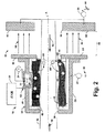
本発明の1つは、イオンビームに対する汚染粒子を容易に取り除くためのシステムおよび方法に関する。イオンビームは、イオンビームの粒子と異なる極性に荷電された粒子が存在する領域の中を移動する。この粒子が荷電される場所よりも下流に電界を発生して、この電界によってイオンビームの流れとともに移動する汚染粒子をイオンビーム流れから離れる方向に向かわせるようにする。電界はまた、イオンビームを所望レベルに加速するための加速領域を与える。その結果、本発明によれば、粒子は、イオンビームの移動方向から離れる、即ち、取り除くことができる。これにより、ワークピースの汚染を軽減する。
本発明のシステム及び方法は、イオンビームに対して汚染粒子を取り除くためのシステム及び方法を提供するためのイオンビーム処理の分野に用いることができる。
Claims (8)
- イオンビームに伴う粒子の移送を抑止するためのシステムであって、
イオンビーム(16)の極性と異なる極性に前記粒子を荷電するための粒子荷電システム(12)と、
この粒子荷電システム(12)に対して下流に電界(50)を発生して、この電界(50)がイオンビーム(16)内に置かれた荷電粒子を前記イオンビーム(16)の移動方向(18)から離れるように作動させる電界発生器(52)とを含み、
前記粒子荷電システム(12)は、イオンビーム(16)が移動する領域内に電子を供給する電子発生装置を含み、前記電子が粒子を負に荷電させ、
前記電子発生装置は、前記粒子を負に荷電する領域内に電子を放出するプラズマ電子フラッド装置(20,22,24)を含み、前記電界(50)が、電子および負電荷の粒子に力を作用させ、前記電子および負電荷の粒子をイオンビームの移動方向から離れるように強制し、
前記粒子荷電システム(12)は、前記領域を規定する内側表面を有する、伸長した側壁部分(30)を含み、さらに、前記粒子荷電システム(12)は、前記領域中の電子の密度を増加するために、前記側壁部分(30)の内側表面に位置する、少なくとも1つの永久磁石(48)を含んでいることを特徴とするシステム。
- 前記電界発生器(52)は、前記イオンビーム(16)の移動方向(18)にほぼ平行な方向(62)に電界(50)を発生し、この電界(50)は、イオンビーム(16)を前記移動方向(18)に加速することを特徴とする請求項1記載のシステム。
- 前記電界発生器(52)は、空間に離間しかつ互いに向き合うように配置された第1、第2の電極(38,52)をさらに含み、前記電界(50)の向きがイオンビームの移動方向(18)にほぼ一致することを特徴とする請求項1記載のシステム。
- 前記電界(50)は、イオンビーム(16)内の複数のイオンに力を作用し、イオンを所定のレベルに加速することを特徴とする請求項3記載のシステム。
- 請求項2または請求項3に記載のシステムであって、
前記粒子荷電システム(12)の前記電子発生装置が、イオンビームを取り囲むプラズマ領域内にプラズマを供給しており、
前記プラズマ領域内に置かれた粒子が負に荷電され、前記電界(50)が、前記イオンビーム(16)内に置かれた前記負に荷電された粒子を、前記イオンビーム(16)の移動方向から離れるように作動させることを特徴とするシステム。
- イオン注入ステーション(216)に配置される基板(W)を処理するために、イオン(106)を放出するイオン源(104,210)と、
所定質量のイオンを注入軌道に偏向するための分析磁石装置(212)と、
該分析磁石装置(202)から偏向したイオンと共に粒子を運搬しないように、請求項1ないし3のいずれかに記載の粒子の移送を抑止するためのシステムからなる粒子除去システム(202)と、
前記粒子除去システム(202)からのイオンを処理するために前記イオン注入ステーション(216)において支持される基板(W)とを含み、これにより、この基板(W)における粒子汚染が軽減されることを特徴とするイオン注入システム。
- 第1電極(256)は、第2電極(260)に対して上流側に配置されており、この第1電極(256)は、粒子荷電システムの下流端に連結して作動することを特徴とする請求項6記載のシステム。
- イオンビームに伴う粒子の移送を抑止するための方法であって、
汚染した粒子を負に荷電するために前記イオンビームが移動する領域内に電子(320)を注入する工程と、
荷電された前記汚染した粒子をイオンビームの移動方向から離れるように強制するために作動可能な電界(330)を発生する工程とを有し、
前記電界を発生する工程は、イオンビームの移動方向にほぼ平行な電界(330)を発生し、さらに、イオンビームの移動方向にイオンビーム(350)を加速するステップを含み、そして、前記領域の外側境界線の近くに磁界を発生して、領域内の電子の密度を改善することを特徴とする方法。
Applications Claiming Priority (3)
| Application Number | Priority Date | Filing Date | Title |
|---|---|---|---|
| US09/654,379 | 2000-09-01 | ||
| US09/654,379 US6476399B1 (en) | 2000-09-01 | 2000-09-01 | System and method for removing contaminant particles relative to an ion beam |
| PCT/GB2001/003709 WO2002019376A2 (en) | 2000-09-01 | 2001-08-17 | System and method for removing contaminant particles relative to an ion beam |
Publications (2)
| Publication Number | Publication Date |
|---|---|
| JP2004508666A JP2004508666A (ja) | 2004-03-18 |
| JP5224014B2 true JP5224014B2 (ja) | 2013-07-03 |
Family
ID=24624619
Family Applications (1)
| Application Number | Title | Priority Date | Filing Date |
|---|---|---|---|
| JP2002524184A Expired - Lifetime JP5224014B2 (ja) | 2000-09-01 | 2001-08-17 | イオンビームに対して汚染粒子を除去するためのシステム及び方法 |
Country Status (8)
| Country | Link |
|---|---|
| US (1) | US6476399B1 (ja) |
| EP (1) | EP1314180A2 (ja) |
| JP (1) | JP5224014B2 (ja) |
| KR (1) | KR100904313B1 (ja) |
| CN (1) | CN100375218C (ja) |
| AU (1) | AU2001279952A1 (ja) |
| TW (1) | TW497159B (ja) |
| WO (1) | WO2002019376A2 (ja) |
Families Citing this family (17)
| Publication number | Priority date | Publication date | Assignee | Title |
|---|---|---|---|---|
| WO2001043157A1 (en) * | 1999-12-13 | 2001-06-14 | Semequip, Inc. | Ion implantation ion source, system and method |
| JP2004134354A (ja) * | 2002-08-13 | 2004-04-30 | Nissin Electric Co Ltd | 熱電子発生源およびそれを備えるイオンビーム照射装置 |
| US20040227106A1 (en) * | 2003-05-13 | 2004-11-18 | Halling Alfred M. | System and methods for ion beam containment using localized electrostatic fields in an ion beam passageway |
| US7820981B2 (en) | 2003-12-12 | 2010-10-26 | Semequip, Inc. | Method and apparatus for extending equipment uptime in ion implantation |
| US7075030B2 (en) * | 2004-08-30 | 2006-07-11 | Brookhaven Science Associates, Llc | Shielded beam delivery apparatus and method |
| US7402816B2 (en) * | 2004-11-19 | 2008-07-22 | Varian Semiconductor Equipment Associates, Inc. | Electron injection in ion implanter magnets |
| US20070278417A1 (en) * | 2005-07-01 | 2007-12-06 | Horsky Thomas N | Ion implantation ion source, system and method |
| KR100671158B1 (ko) * | 2005-08-11 | 2007-01-17 | 동부일렉트로닉스 주식회사 | 파티클 제거 장치 및 이를 포함하는 이온 주입 장치 |
| US7675046B2 (en) * | 2006-09-27 | 2010-03-09 | Varian Semiconductor Equipment Associates, Inc | Terminal structure of an ion implanter |
| US7800083B2 (en) * | 2007-11-06 | 2010-09-21 | Axcelis Technologies, Inc. | Plasma electron flood for ion beam implanter |
| US8941968B2 (en) * | 2010-06-08 | 2015-01-27 | Axcelis Technologies, Inc. | Heated electrostatic chuck including mechanical clamp capability at high temperature |
| CN102486986B (zh) * | 2010-12-03 | 2015-06-03 | 中芯国际集成电路制造(北京)有限公司 | 等离子清洁装置 |
| CN102677160B (zh) * | 2012-05-29 | 2015-02-04 | 江苏中电振华晶体技术有限公司 | 一种泡生法生长蓝宝石的引晶方法及系统 |
| US9209032B2 (en) * | 2013-03-15 | 2015-12-08 | Tokyo Electron Limited | Electric pressure systems for control of plasma properties and uniformity |
| US9721750B2 (en) | 2015-07-28 | 2017-08-01 | Varian Semiconductor Equipment Associates, Inc. | Controlling contamination particle trajectory from a beam-line electrostatic element |
| US9685298B1 (en) * | 2016-02-01 | 2017-06-20 | Varian Semiconductor Equipment Associates, Inc. | Apparatus and method for contamination control in ion beam apparatus |
| CA3089085A1 (en) * | 2018-01-22 | 2019-07-25 | Riken | Accelerator and accelerator system |
Family Cites Families (22)
| Publication number | Priority date | Publication date | Assignee | Title |
|---|---|---|---|---|
| US4683922A (en) | 1986-01-24 | 1987-08-04 | Allied Corporation | Particle deflector and method of distributing dissimilar particles |
| US4825087A (en) * | 1987-05-13 | 1989-04-25 | Applied Materials, Inc. | System and methods for wafer charge reduction for ion implantation |
| JP2716518B2 (ja) * | 1989-04-21 | 1998-02-18 | 東京エレクトロン株式会社 | イオン注入装置及びイオン注入方法 |
| JPH0462747A (ja) * | 1990-07-02 | 1992-02-27 | Nippon Telegr & Teleph Corp <Ntt> | 酸素2価イオンの取出し方法 |
| US5134299A (en) | 1991-03-13 | 1992-07-28 | Eaton Corporation | Ion beam implantation method and apparatus for particulate control |
| JP3123123B2 (ja) * | 1991-06-05 | 2001-01-09 | 日新電機株式会社 | イオン注入装置 |
| US5466929A (en) * | 1992-02-21 | 1995-11-14 | Hitachi, Ltd. | Apparatus and method for suppressing electrification of sample in charged beam irradiation apparatus |
| JPH05234562A (ja) * | 1992-02-21 | 1993-09-10 | Hitachi Ltd | イオンビーム中性化装置 |
| JP3054302B2 (ja) | 1992-12-02 | 2000-06-19 | アプライド マテリアルズ インコーポレイテッド | イオン注入中の半導体ウェハにおける帯電を低減するプラズマ放出システム |
| JPH06243816A (ja) * | 1993-02-18 | 1994-09-02 | Nissin Electric Co Ltd | イオン注入装置 |
| JP3395265B2 (ja) * | 1993-06-30 | 2003-04-07 | ソニー株式会社 | イオン注入装置における中性粒子除去方法及びイオン注入装置 |
| US5384465A (en) * | 1993-09-17 | 1995-01-24 | Applied Materials, Inc. | Spectrum analyzer in an ion implanter |
| GB2343546B (en) * | 1995-11-08 | 2000-06-21 | Applied Materials Inc | An ion implanter with deceleration lens assembly |
| US5656092A (en) | 1995-12-18 | 1997-08-12 | Eaton Corporation | Apparatus for capturing and removing contaminant particles from an interior region of an ion implanter |
| US5760409A (en) * | 1996-06-14 | 1998-06-02 | Eaton Corporation | Dose control for use in an ion implanter |
| US5703375A (en) * | 1996-08-02 | 1997-12-30 | Eaton Corporation | Method and apparatus for ion beam neutralization |
| GB9710380D0 (en) * | 1997-05-20 | 1997-07-16 | Applied Materials Inc | Electron flood apparatus for neutralising charge build-up on a substrate during ion implantation |
| JP3627206B2 (ja) * | 1997-11-28 | 2005-03-09 | 住友イートンノバ株式会社 | イオン注入装置及びイオン注入方法 |
| US6135128A (en) * | 1998-03-27 | 2000-10-24 | Eaton Corporation | Method for in-process cleaning of an ion source |
| KR100282492B1 (ko) * | 1998-04-13 | 2001-02-15 | 윤종용 | 불순물차단장치를구비하는이온주입장치 |
| US6359286B1 (en) * | 1998-07-10 | 2002-03-19 | Applied Materials, Inc. | Method and apparatus for neutralizing space charge in an ion beam |
| JP2000133197A (ja) * | 1998-10-30 | 2000-05-12 | Applied Materials Inc | イオン注入装置 |
-
2000
- 2000-09-01 US US09/654,379 patent/US6476399B1/en not_active Expired - Lifetime
-
2001
- 2001-08-17 AU AU2001279952A patent/AU2001279952A1/en not_active Abandoned
- 2001-08-17 EP EP01958225A patent/EP1314180A2/en not_active Withdrawn
- 2001-08-17 KR KR1020037003081A patent/KR100904313B1/ko not_active Expired - Lifetime
- 2001-08-17 CN CNB018185002A patent/CN100375218C/zh not_active Expired - Fee Related
- 2001-08-17 JP JP2002524184A patent/JP5224014B2/ja not_active Expired - Lifetime
- 2001-08-17 WO PCT/GB2001/003709 patent/WO2002019376A2/en not_active Ceased
- 2001-08-21 TW TW090120483A patent/TW497159B/zh not_active IP Right Cessation
Also Published As
| Publication number | Publication date |
|---|---|
| EP1314180A2 (en) | 2003-05-28 |
| WO2002019376A2 (en) | 2002-03-07 |
| CN1473349A (zh) | 2004-02-04 |
| US6476399B1 (en) | 2002-11-05 |
| TW497159B (en) | 2002-08-01 |
| KR20030029897A (ko) | 2003-04-16 |
| AU2001279952A1 (en) | 2002-03-13 |
| JP2004508666A (ja) | 2004-03-18 |
| WO2002019376A3 (en) | 2002-05-10 |
| CN100375218C (zh) | 2008-03-12 |
| KR100904313B1 (ko) | 2009-06-23 |
Similar Documents
| Publication | Publication Date | Title |
|---|---|---|
| KR100855135B1 (ko) | 이온빔 내에 유입된 입자에 대한 정전기 트랩 | |
| JP4117507B2 (ja) | イオン注入装置、その内側表面からの汚染物質の除去方法とそのための除去装置 | |
| KR101236563B1 (ko) | 하전된 빔 덤프 및 입자 어트랙터 | |
| JP5224014B2 (ja) | イオンビームに対して汚染粒子を除去するためのシステム及び方法 | |
| KR101564898B1 (ko) | 고 전류 이온 주입을 위한 저 오염, 저 에너지 비임라인 구성물 | |
| JP5120598B2 (ja) | 偏向用の加速/減速ギャップ | |
| US5703375A (en) | Method and apparatus for ion beam neutralization | |
| JPH09129172A (ja) | 自浄式イオンビーム中和装置及びその内部表面に付着した汚染物質を清浄する方法 | |
| KR100855134B1 (ko) | 이온 빔내로 끌려오는 입자들을 제거하기 위한 장치 및 방법 | |
| JP5519789B2 (ja) | 調節可能であるルーバー加工されたプラズマエレクトロンフラッド筐体 | |
| KR101148048B1 (ko) | 전하 중화 장치 | |
| EP0095879A2 (en) | Apparatus and method for working surfaces with a low energy high intensity ion beam |
Legal Events
| Date | Code | Title | Description |
|---|---|---|---|
| A621 | Written request for application examination |
Free format text: JAPANESE INTERMEDIATE CODE: A621 Effective date: 20080814 |
|
| A977 | Report on retrieval |
Free format text: JAPANESE INTERMEDIATE CODE: A971007 Effective date: 20110721 |
|
| A131 | Notification of reasons for refusal |
Free format text: JAPANESE INTERMEDIATE CODE: A131 Effective date: 20110727 |
|
| A601 | Written request for extension of time |
Free format text: JAPANESE INTERMEDIATE CODE: A601 Effective date: 20111026 |
|
| A602 | Written permission of extension of time |
Free format text: JAPANESE INTERMEDIATE CODE: A602 Effective date: 20111102 |
|
| A521 | Request for written amendment filed |
Free format text: JAPANESE INTERMEDIATE CODE: A523 Effective date: 20111111 |
|
| A131 | Notification of reasons for refusal |
Free format text: JAPANESE INTERMEDIATE CODE: A131 Effective date: 20120919 |
|
| A601 | Written request for extension of time |
Free format text: JAPANESE INTERMEDIATE CODE: A601 Effective date: 20121218 |
|
| A602 | Written permission of extension of time |
Free format text: JAPANESE INTERMEDIATE CODE: A602 Effective date: 20121226 |
|
| A521 | Request for written amendment filed |
Free format text: JAPANESE INTERMEDIATE CODE: A523 Effective date: 20130108 |
|
| TRDD | Decision of grant or rejection written | ||
| A01 | Written decision to grant a patent or to grant a registration (utility model) |
Free format text: JAPANESE INTERMEDIATE CODE: A01 Effective date: 20130130 |
|
| A61 | First payment of annual fees (during grant procedure) |
Free format text: JAPANESE INTERMEDIATE CODE: A61 Effective date: 20130226 |
|
| R150 | Certificate of patent or registration of utility model |
Free format text: JAPANESE INTERMEDIATE CODE: R150 Ref document number: 5224014 Country of ref document: JP Free format text: JAPANESE INTERMEDIATE CODE: R150 |
|
| FPAY | Renewal fee payment (event date is renewal date of database) |
Free format text: PAYMENT UNTIL: 20160322 Year of fee payment: 3 |
|
| R250 | Receipt of annual fees |
Free format text: JAPANESE INTERMEDIATE CODE: R250 |
|
| R250 | Receipt of annual fees |
Free format text: JAPANESE INTERMEDIATE CODE: R250 |
|
| R250 | Receipt of annual fees |
Free format text: JAPANESE INTERMEDIATE CODE: R250 |
|
| R250 | Receipt of annual fees |
Free format text: JAPANESE INTERMEDIATE CODE: R250 |
|
| R250 | Receipt of annual fees |
Free format text: JAPANESE INTERMEDIATE CODE: R250 |
|
| R250 | Receipt of annual fees |
Free format text: JAPANESE INTERMEDIATE CODE: R250 |
|
| EXPY | Cancellation because of completion of term |