JP5227900B2 - 半導体装置の作製方法 - Google Patents
半導体装置の作製方法 Download PDFInfo
- Publication number
- JP5227900B2 JP5227900B2 JP2009136617A JP2009136617A JP5227900B2 JP 5227900 B2 JP5227900 B2 JP 5227900B2 JP 2009136617 A JP2009136617 A JP 2009136617A JP 2009136617 A JP2009136617 A JP 2009136617A JP 5227900 B2 JP5227900 B2 JP 5227900B2
- Authority
- JP
- Japan
- Prior art keywords
- substrate
- laser
- film
- laser beams
- light
- Prior art date
- Legal status (The legal status is an assumption and is not a legal conclusion. Google has not performed a legal analysis and makes no representation as to the accuracy of the status listed.)
- Expired - Fee Related
Links
Images










Classifications
-
- H—ELECTRICITY
- H10—SEMICONDUCTOR DEVICES; ELECTRIC SOLID-STATE DEVICES NOT OTHERWISE PROVIDED FOR
- H10P—GENERIC PROCESSES OR APPARATUS FOR THE MANUFACTURE OR TREATMENT OF DEVICES COVERED BY CLASS H10
- H10P14/00—Formation of materials, e.g. in the shape of layers or pillars
- H10P14/20—Formation of materials, e.g. in the shape of layers or pillars of semiconductor materials
- H10P14/38—Formation of materials, e.g. in the shape of layers or pillars of semiconductor materials characterised by treatments done after the formation of the materials
- H10P14/3802—Crystallisation or recrystallisation of non-monocrystalline semiconductor materials, e.g. regrowth
- H10P14/3808—Crystallisation or recrystallisation of non-monocrystalline semiconductor materials, e.g. regrowth using laser beams
- H10P14/3814—Continuous wave laser beam
-
- B—PERFORMING OPERATIONS; TRANSPORTING
- B23—MACHINE TOOLS; METAL-WORKING NOT OTHERWISE PROVIDED FOR
- B23K—SOLDERING OR UNSOLDERING; WELDING; CLADDING OR PLATING BY SOLDERING OR WELDING; CUTTING BY APPLYING HEAT LOCALLY, e.g. FLAME CUTTING; WORKING BY LASER BEAM
- B23K26/00—Working by laser beam, e.g. welding, cutting or boring
- B23K26/02—Positioning or observing the workpiece, e.g. with respect to the point of impact; Aligning, aiming or focusing the laser beam
- B23K26/06—Shaping the laser beam, e.g. by masks or multi-focusing
- B23K26/064—Shaping the laser beam, e.g. by masks or multi-focusing by means of optical elements, e.g. lenses, mirrors or prisms
- B23K26/066—Shaping the laser beam, e.g. by masks or multi-focusing by means of optical elements, e.g. lenses, mirrors or prisms by using masks
-
- B—PERFORMING OPERATIONS; TRANSPORTING
- B23—MACHINE TOOLS; METAL-WORKING NOT OTHERWISE PROVIDED FOR
- B23K—SOLDERING OR UNSOLDERING; WELDING; CLADDING OR PLATING BY SOLDERING OR WELDING; CUTTING BY APPLYING HEAT LOCALLY, e.g. FLAME CUTTING; WORKING BY LASER BEAM
- B23K26/00—Working by laser beam, e.g. welding, cutting or boring
- B23K26/02—Positioning or observing the workpiece, e.g. with respect to the point of impact; Aligning, aiming or focusing the laser beam
- B23K26/06—Shaping the laser beam, e.g. by masks or multi-focusing
- B23K26/067—Dividing the beam into multiple beams, e.g. multi-focusing
-
- B—PERFORMING OPERATIONS; TRANSPORTING
- B23—MACHINE TOOLS; METAL-WORKING NOT OTHERWISE PROVIDED FOR
- B23K—SOLDERING OR UNSOLDERING; WELDING; CLADDING OR PLATING BY SOLDERING OR WELDING; CUTTING BY APPLYING HEAT LOCALLY, e.g. FLAME CUTTING; WORKING BY LASER BEAM
- B23K26/00—Working by laser beam, e.g. welding, cutting or boring
- B23K26/02—Positioning or observing the workpiece, e.g. with respect to the point of impact; Aligning, aiming or focusing the laser beam
- B23K26/06—Shaping the laser beam, e.g. by masks or multi-focusing
- B23K26/067—Dividing the beam into multiple beams, e.g. multi-focusing
- B23K26/0676—Dividing the beam into multiple beams, e.g. multi-focusing into dependently operating sub-beams, e.g. an array of spots with fixed spatial relationship or for performing simultaneously identical operations
-
- B—PERFORMING OPERATIONS; TRANSPORTING
- B23—MACHINE TOOLS; METAL-WORKING NOT OTHERWISE PROVIDED FOR
- B23K—SOLDERING OR UNSOLDERING; WELDING; CLADDING OR PLATING BY SOLDERING OR WELDING; CUTTING BY APPLYING HEAT LOCALLY, e.g. FLAME CUTTING; WORKING BY LASER BEAM
- B23K26/00—Working by laser beam, e.g. welding, cutting or boring
- B23K26/02—Positioning or observing the workpiece, e.g. with respect to the point of impact; Aligning, aiming or focusing the laser beam
- B23K26/06—Shaping the laser beam, e.g. by masks or multi-focusing
- B23K26/073—Shaping the laser spot
- B23K26/0732—Shaping the laser spot into a rectangular shape
-
- B—PERFORMING OPERATIONS; TRANSPORTING
- B23—MACHINE TOOLS; METAL-WORKING NOT OTHERWISE PROVIDED FOR
- B23K—SOLDERING OR UNSOLDERING; WELDING; CLADDING OR PLATING BY SOLDERING OR WELDING; CUTTING BY APPLYING HEAT LOCALLY, e.g. FLAME CUTTING; WORKING BY LASER BEAM
- B23K26/00—Working by laser beam, e.g. welding, cutting or boring
- B23K26/02—Positioning or observing the workpiece, e.g. with respect to the point of impact; Aligning, aiming or focusing the laser beam
- B23K26/06—Shaping the laser beam, e.g. by masks or multi-focusing
- B23K26/073—Shaping the laser spot
- B23K26/0736—Shaping the laser spot into an oval shape, e.g. elliptic shape
-
- B—PERFORMING OPERATIONS; TRANSPORTING
- B23—MACHINE TOOLS; METAL-WORKING NOT OTHERWISE PROVIDED FOR
- B23K—SOLDERING OR UNSOLDERING; WELDING; CLADDING OR PLATING BY SOLDERING OR WELDING; CUTTING BY APPLYING HEAT LOCALLY, e.g. FLAME CUTTING; WORKING BY LASER BEAM
- B23K26/00—Working by laser beam, e.g. welding, cutting or boring
- B23K26/08—Devices involving relative movement between laser beam and workpiece
- B23K26/10—Devices involving relative movement between laser beam and workpiece using a fixed support, i.e. involving moving the laser beam
-
- H—ELECTRICITY
- H01—ELECTRIC ELEMENTS
- H01S—DEVICES USING THE PROCESS OF LIGHT AMPLIFICATION BY STIMULATED EMISSION OF RADIATION [LASER] TO AMPLIFY OR GENERATE LIGHT; DEVICES USING STIMULATED EMISSION OF ELECTROMAGNETIC RADIATION IN WAVE RANGES OTHER THAN OPTICAL
- H01S3/00—Lasers, i.e. devices using stimulated emission of electromagnetic radiation in the infrared, visible or ultraviolet wave range
- H01S3/005—Optical devices external to the laser cavity, specially adapted for lasers, e.g. for homogenisation of the beam or for manipulating laser pulses, e.g. pulse shaping
- H01S3/0071—Beam steering, e.g. whereby a mirror outside the cavity is present to change the beam direction
-
- H—ELECTRICITY
- H10—SEMICONDUCTOR DEVICES; ELECTRIC SOLID-STATE DEVICES NOT OTHERWISE PROVIDED FOR
- H10P—GENERIC PROCESSES OR APPARATUS FOR THE MANUFACTURE OR TREATMENT OF DEVICES COVERED BY CLASS H10
- H10P14/00—Formation of materials, e.g. in the shape of layers or pillars
- H10P14/20—Formation of materials, e.g. in the shape of layers or pillars of semiconductor materials
- H10P14/29—Formation of materials, e.g. in the shape of layers or pillars of semiconductor materials characterised by the substrates
- H10P14/2901—Materials
- H10P14/2902—Materials being Group IVA materials
- H10P14/2905—Silicon, silicon germanium or germanium
-
- H—ELECTRICITY
- H10—SEMICONDUCTOR DEVICES; ELECTRIC SOLID-STATE DEVICES NOT OTHERWISE PROVIDED FOR
- H10P—GENERIC PROCESSES OR APPARATUS FOR THE MANUFACTURE OR TREATMENT OF DEVICES COVERED BY CLASS H10
- H10P14/00—Formation of materials, e.g. in the shape of layers or pillars
- H10P14/20—Formation of materials, e.g. in the shape of layers or pillars of semiconductor materials
- H10P14/29—Formation of materials, e.g. in the shape of layers or pillars of semiconductor materials characterised by the substrates
- H10P14/2901—Materials
- H10P14/2921—Materials being crystalline insulating materials
-
- H—ELECTRICITY
- H10—SEMICONDUCTOR DEVICES; ELECTRIC SOLID-STATE DEVICES NOT OTHERWISE PROVIDED FOR
- H10P—GENERIC PROCESSES OR APPARATUS FOR THE MANUFACTURE OR TREATMENT OF DEVICES COVERED BY CLASS H10
- H10P14/00—Formation of materials, e.g. in the shape of layers or pillars
- H10P14/20—Formation of materials, e.g. in the shape of layers or pillars of semiconductor materials
- H10P14/29—Formation of materials, e.g. in the shape of layers or pillars of semiconductor materials characterised by the substrates
- H10P14/2901—Materials
- H10P14/2922—Materials being non-crystalline insulating materials, e.g. glass or polymers
-
- H—ELECTRICITY
- H10—SEMICONDUCTOR DEVICES; ELECTRIC SOLID-STATE DEVICES NOT OTHERWISE PROVIDED FOR
- H10P—GENERIC PROCESSES OR APPARATUS FOR THE MANUFACTURE OR TREATMENT OF DEVICES COVERED BY CLASS H10
- H10P14/00—Formation of materials, e.g. in the shape of layers or pillars
- H10P14/20—Formation of materials, e.g. in the shape of layers or pillars of semiconductor materials
- H10P14/29—Formation of materials, e.g. in the shape of layers or pillars of semiconductor materials characterised by the substrates
- H10P14/2901—Materials
- H10P14/2923—Materials being conductive materials, e.g. metallic silicides
-
- H—ELECTRICITY
- H10—SEMICONDUCTOR DEVICES; ELECTRIC SOLID-STATE DEVICES NOT OTHERWISE PROVIDED FOR
- H10P—GENERIC PROCESSES OR APPARATUS FOR THE MANUFACTURE OR TREATMENT OF DEVICES COVERED BY CLASS H10
- H10P14/00—Formation of materials, e.g. in the shape of layers or pillars
- H10P14/20—Formation of materials, e.g. in the shape of layers or pillars of semiconductor materials
- H10P14/32—Formation of materials, e.g. in the shape of layers or pillars of semiconductor materials characterised by intermediate layers between substrates and deposited layers
- H10P14/3202—Materials thereof
- H10P14/3238—Materials thereof being insulating materials
-
- H—ELECTRICITY
- H10—SEMICONDUCTOR DEVICES; ELECTRIC SOLID-STATE DEVICES NOT OTHERWISE PROVIDED FOR
- H10P—GENERIC PROCESSES OR APPARATUS FOR THE MANUFACTURE OR TREATMENT OF DEVICES COVERED BY CLASS H10
- H10P14/00—Formation of materials, e.g. in the shape of layers or pillars
- H10P14/20—Formation of materials, e.g. in the shape of layers or pillars of semiconductor materials
- H10P14/32—Formation of materials, e.g. in the shape of layers or pillars of semiconductor materials characterised by intermediate layers between substrates and deposited layers
- H10P14/3242—Structure
- H10P14/3244—Layer structure
- H10P14/3248—Layer structure consisting of two layers
-
- H—ELECTRICITY
- H10—SEMICONDUCTOR DEVICES; ELECTRIC SOLID-STATE DEVICES NOT OTHERWISE PROVIDED FOR
- H10P—GENERIC PROCESSES OR APPARATUS FOR THE MANUFACTURE OR TREATMENT OF DEVICES COVERED BY CLASS H10
- H10P14/00—Formation of materials, e.g. in the shape of layers or pillars
- H10P14/20—Formation of materials, e.g. in the shape of layers or pillars of semiconductor materials
- H10P14/34—Deposited materials, e.g. layers
- H10P14/3402—Deposited materials, e.g. layers characterised by the chemical composition
- H10P14/3404—Deposited materials, e.g. layers characterised by the chemical composition being Group IVA materials
- H10P14/3411—Silicon, silicon germanium or germanium
-
- H—ELECTRICITY
- H10—SEMICONDUCTOR DEVICES; ELECTRIC SOLID-STATE DEVICES NOT OTHERWISE PROVIDED FOR
- H10P—GENERIC PROCESSES OR APPARATUS FOR THE MANUFACTURE OR TREATMENT OF DEVICES COVERED BY CLASS H10
- H10P14/00—Formation of materials, e.g. in the shape of layers or pillars
- H10P14/20—Formation of materials, e.g. in the shape of layers or pillars of semiconductor materials
- H10P14/34—Deposited materials, e.g. layers
- H10P14/3451—Structure
- H10P14/3452—Microstructure
- H10P14/3458—Monocrystalline
-
- H—ELECTRICITY
- H10—SEMICONDUCTOR DEVICES; ELECTRIC SOLID-STATE DEVICES NOT OTHERWISE PROVIDED FOR
- H10P—GENERIC PROCESSES OR APPARATUS FOR THE MANUFACTURE OR TREATMENT OF DEVICES COVERED BY CLASS H10
- H10P14/00—Formation of materials, e.g. in the shape of layers or pillars
- H10P14/20—Formation of materials, e.g. in the shape of layers or pillars of semiconductor materials
- H10P14/38—Formation of materials, e.g. in the shape of layers or pillars of semiconductor materials characterised by treatments done after the formation of the materials
- H10P14/3802—Crystallisation or recrystallisation of non-monocrystalline semiconductor materials, e.g. regrowth
- H10P14/3808—Crystallisation or recrystallisation of non-monocrystalline semiconductor materials, e.g. regrowth using laser beams
- H10P14/381—Beam shaping, e.g. using a mask
-
- H—ELECTRICITY
- H10—SEMICONDUCTOR DEVICES; ELECTRIC SOLID-STATE DEVICES NOT OTHERWISE PROVIDED FOR
- H10P—GENERIC PROCESSES OR APPARATUS FOR THE MANUFACTURE OR TREATMENT OF DEVICES COVERED BY CLASS H10
- H10P14/00—Formation of materials, e.g. in the shape of layers or pillars
- H10P14/20—Formation of materials, e.g. in the shape of layers or pillars of semiconductor materials
- H10P14/38—Formation of materials, e.g. in the shape of layers or pillars of semiconductor materials characterised by treatments done after the formation of the materials
- H10P14/3802—Crystallisation or recrystallisation of non-monocrystalline semiconductor materials, e.g. regrowth
- H10P14/3808—Crystallisation or recrystallisation of non-monocrystalline semiconductor materials, e.g. regrowth using laser beams
- H10P14/3816—Pulsed laser beam
-
- H—ELECTRICITY
- H10—SEMICONDUCTOR DEVICES; ELECTRIC SOLID-STATE DEVICES NOT OTHERWISE PROVIDED FOR
- H10P—GENERIC PROCESSES OR APPARATUS FOR THE MANUFACTURE OR TREATMENT OF DEVICES COVERED BY CLASS H10
- H10P14/00—Formation of materials, e.g. in the shape of layers or pillars
- H10P14/20—Formation of materials, e.g. in the shape of layers or pillars of semiconductor materials
- H10P14/38—Formation of materials, e.g. in the shape of layers or pillars of semiconductor materials characterised by treatments done after the formation of the materials
- H10P14/3802—Crystallisation or recrystallisation of non-monocrystalline semiconductor materials, e.g. regrowth
- H10P14/382—Scanning of a beam
-
- B—PERFORMING OPERATIONS; TRANSPORTING
- B23—MACHINE TOOLS; METAL-WORKING NOT OTHERWISE PROVIDED FOR
- B23K—SOLDERING OR UNSOLDERING; WELDING; CLADDING OR PLATING BY SOLDERING OR WELDING; CUTTING BY APPLYING HEAT LOCALLY, e.g. FLAME CUTTING; WORKING BY LASER BEAM
- B23K2101/00—Articles made by soldering, welding or cutting
- B23K2101/36—Electric or electronic devices
- B23K2101/40—Semiconductor devices
Landscapes
- Physics & Mathematics (AREA)
- Optics & Photonics (AREA)
- Engineering & Computer Science (AREA)
- Plasma & Fusion (AREA)
- Mechanical Engineering (AREA)
- Electromagnetism (AREA)
- Recrystallisation Techniques (AREA)
- Liquid Crystal (AREA)
- Thin Film Transistor (AREA)
Description
(a)従来のTFTの作製プロセスに適合した、簡単な方法である。
(b)照射面においてエネルギー分布が同一なレーザ光を照射することができる。
(c)スループットを向上させることを可能とする。これは、大面積基板の場合に特に有効である。
(d)単結晶に近い結晶粒を有する半導体膜を形成することができる。
(e)以上の利点を満たした上で、アクティブマトリクス型の液晶表示装置に代表される半導体装置において、半導体装置の動作特性および信頼性の向上を実現することができる。さらに、半導体装置の製造コストの低減を実現することができる。
を満たす入射角φより大きければ、干渉は起こらない。つまり、φ≧arcsin(W/2d)
のとき、干渉は起こらない。そのため、入射角φより大きい角度で入射させる場合には、複数のレーザ光の入射角を厳密に合わせなくてもよい。
を移動させれば、基板に対するレーザ光の入射角を変えることなく、108で示す方向へ照射することができる。106で示す方向への照射が終了すると、107で示す方向へステージ(または基板)を移動させ、レーザ光を照射しながら108で示す方向へステージ(または基板)を移動させれば、106で示す方向へ照射することができる。これらの移動を繰り返すことで、基板全面にレーザ光が照射される。
(図6(C))ここでは、エッチングガスにCF4とCl2とO2とを用い、W膜を選択的にエッチングする。この時、第2のエッチング処理により第2の導電層428b〜433bを形成する。一方、第1の導電層417a〜422aは、ほとんどエッチングされず、第2の形状の導電層428〜433を形成する。
例えば、TaN膜上にAlやCuを形成し、さらにTi膜を形成した積層膜をパターニングして配線を形成してもよい。(図8)
バンク712は100〜400nmの珪素を含む絶縁膜もしくは有機樹脂膜をパターニングして形成すれば良い。
Alq3にキナクリドン、ペリレンもしくはDCM1といった蛍光色素を添加することで発光色を制御することができる。
を作製することができる。即ち、それら電気光学装置を表示部に組み込んだ様々な電子機器に本発明を適用できる。
本発明は表示部3402に適用することができる。
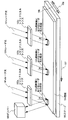
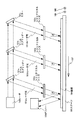
また106、107、108には基板が移動する方向が示されている。
Claims (2)
- 基板上に半導体膜を形成する工程と、
複数のレーザ光の照射位置を第1の方向へ移動させながら、前記半導体膜の複数の第1の領域を結晶化させる工程と、
前記複数のレーザ光の照射位置を第2の方向へ移動させる工程と、
前記複数のレーザ光の照射位置を第3の方向へ移動させながら、前記半導体膜の複数の第2の領域を結晶化させる工程と、を有し、
前記第3の方向は、前記第1の方向と逆方向であり、
前記第2の方向は、前記第1の方向と垂直な方向であり、
前記複数のレーザ光は前記基板の表面に対して斜め方向から同じ角度で入射し、
前記基板の裏面側に第1の反射板を有し、
前記基板の表面側に第2の反射板を有し、
前記基板を通過した前記複数のレーザ光が前記第1の反射板で反射して前記半導体膜に再度照射され、
前記第1の反射板で反射して前記半導体膜を通過した前記複数のレーザ光が前記第2の反射板で反射して前記半導体膜に再度照射されることを特徴とする半導体装置の作製方法。 - 基板上に半導体膜を形成する工程と、
複数のレーザ光の照射位置を第1の方向へ移動させながら、前記半導体膜の複数の第1の領域を結晶化させる工程と、
前記複数のレーザ光の照射位置を第3の方向へ移動させながら、前記複数の第1の領域を結晶化させる工程と、
前記複数のレーザ光の照射位置を第2の方向へ移動させる工程と、
前記複数のレーザ光の照射位置を前記第1の方向へ移動させながら、前記半導体膜の複数の第2の領域を結晶化させる工程と、
前記複数のレーザ光の照射位置を前記第3の方向へ移動させながら、前記複数の第2の領域を結晶化させる工程と、を有し、
前記第3の方向は、前記第1の方向と逆方向であり、
前記第2の方向は、前記第1の方向と垂直な方向であり、
前記複数のレーザ光は前記基板の表面に対して斜め方向から同じ角度で入射し、
前記基板の裏面側に第1の反射板を有し、
前記基板の表面側に第2の反射板を有し、
前記基板を通過した前記複数のレーザ光が前記第1の反射板で反射して前記半導体膜に再度照射され、
前記第1の反射板で反射して前記半導体膜を通過した前記複数のレーザ光が前記第2の反射板で反射して前記半導体膜に再度照射されることを特徴とする半導体装置の作製方法。
Priority Applications (1)
| Application Number | Priority Date | Filing Date | Title |
|---|---|---|---|
| JP2009136617A JP5227900B2 (ja) | 2001-08-03 | 2009-06-05 | 半導体装置の作製方法 |
Applications Claiming Priority (3)
| Application Number | Priority Date | Filing Date | Title |
|---|---|---|---|
| JP2001237097 | 2001-08-03 | ||
| JP2001237097 | 2001-08-03 | ||
| JP2009136617A JP5227900B2 (ja) | 2001-08-03 | 2009-06-05 | 半導体装置の作製方法 |
Related Parent Applications (1)
| Application Number | Title | Priority Date | Filing Date |
|---|---|---|---|
| JP2002225628A Division JP2003151916A (ja) | 2001-08-03 | 2002-08-02 | レーザ照射装置およびレーザ照射方法、並びに半導体装置の作製方法 |
Publications (2)
| Publication Number | Publication Date |
|---|---|
| JP2009206521A JP2009206521A (ja) | 2009-09-10 |
| JP5227900B2 true JP5227900B2 (ja) | 2013-07-03 |
Family
ID=19068236
Family Applications (1)
| Application Number | Title | Priority Date | Filing Date |
|---|---|---|---|
| JP2009136617A Expired - Fee Related JP5227900B2 (ja) | 2001-08-03 | 2009-06-05 | 半導体装置の作製方法 |
Country Status (7)
| Country | Link |
|---|---|
| US (3) | US7868267B2 (ja) |
| JP (1) | JP5227900B2 (ja) |
| KR (3) | KR20030011724A (ja) |
| CN (3) | CN101879658B (ja) |
| MY (1) | MY157663A (ja) |
| SG (2) | SG121721A1 (ja) |
| TW (1) | TW552645B (ja) |
Families Citing this family (60)
| Publication number | Priority date | Publication date | Assignee | Title |
|---|---|---|---|---|
| SG113399A1 (en) | 2000-12-27 | 2005-08-29 | Semiconductor Energy Lab | Laser annealing method and semiconductor device fabricating method |
| US6809012B2 (en) * | 2001-01-18 | 2004-10-26 | Semiconductor Energy Laboratory Co., Ltd. | Method of making a thin film transistor using laser annealing |
| TW552645B (en) * | 2001-08-03 | 2003-09-11 | Semiconductor Energy Lab | Laser irradiating device, laser irradiating method and manufacturing method of semiconductor device |
| KR100885904B1 (ko) * | 2001-08-10 | 2009-02-26 | 가부시키가이샤 한도오따이 에네루기 켄큐쇼 | 레이저 어닐링장치 및 반도체장치의 제작방법 |
| JP4209606B2 (ja) * | 2001-08-17 | 2009-01-14 | 株式会社半導体エネルギー研究所 | 半導体装置の作製方法 |
| TWI282126B (en) * | 2001-08-30 | 2007-06-01 | Semiconductor Energy Lab | Method for manufacturing semiconductor device |
| US7317205B2 (en) * | 2001-09-10 | 2008-01-08 | Semiconductor Energy Laboratory Co., Ltd. | Light emitting device and method of manufacturing a semiconductor device |
| US7112517B2 (en) | 2001-09-10 | 2006-09-26 | Semiconductor Energy Laboratory Co., Ltd. | Laser treatment device, laser treatment method, and semiconductor device fabrication method |
| JP4397571B2 (ja) * | 2001-09-25 | 2010-01-13 | 株式会社半導体エネルギー研究所 | レーザ照射方法およびレーザ照射装置、並びに半導体装置の作製方法 |
| US7026227B2 (en) * | 2001-11-16 | 2006-04-11 | Semiconductor Energy Laboratory Co., Ltd. | Method of irradiating a laser beam, and method of fabricating semiconductor devices |
| TWI291729B (en) | 2001-11-22 | 2007-12-21 | Semiconductor Energy Lab | A semiconductor fabricating apparatus |
| US7105048B2 (en) * | 2001-11-30 | 2006-09-12 | Semiconductor Energy Laboratory Co., Ltd. | Laser irradiation apparatus |
| KR100967824B1 (ko) * | 2001-11-30 | 2010-07-05 | 가부시키가이샤 한도오따이 에네루기 켄큐쇼 | 반도체장치의 제작방법 |
| US7133737B2 (en) | 2001-11-30 | 2006-11-07 | Semiconductor Energy Laboratory Co., Ltd. | Program for controlling laser apparatus and recording medium for recording program for controlling laser apparatus and capable of being read out by computer |
| US7214573B2 (en) | 2001-12-11 | 2007-05-08 | Semiconductor Energy Laboratory Co., Ltd. | Method of manufacturing a semiconductor device that includes patterning sub-islands |
| US7113527B2 (en) * | 2001-12-21 | 2006-09-26 | Semiconductor Energy Laboratory Co., Ltd. | Method and apparatus for laser irradiation and manufacturing method of semiconductor device |
| US6984573B2 (en) * | 2002-06-14 | 2006-01-10 | Semiconductor Energy Laboratory Co., Ltd. | Laser irradiation method and apparatus |
| JP2004119971A (ja) * | 2002-09-04 | 2004-04-15 | Sharp Corp | レーザ加工方法およびレーザ加工装置 |
| EP1400832B1 (en) * | 2002-09-19 | 2014-10-22 | Semiconductor Energy Laboratory Co., Ltd. | Beam homogenizer and laser irradiation apparatus and method of manufacturing semiconductor device |
| JP2004200358A (ja) * | 2002-12-18 | 2004-07-15 | Nikon Corp | 固体撮像素子の色分解装置 |
| KR100956339B1 (ko) * | 2003-02-25 | 2010-05-06 | 삼성전자주식회사 | 규소 결정화 시스템 및 규소 결정화 방법 |
| KR100992120B1 (ko) * | 2003-03-13 | 2010-11-04 | 삼성전자주식회사 | 규소 결정화 시스템 및 규소 결정화 방법 |
| SG137674A1 (en) * | 2003-04-24 | 2007-12-28 | Semiconductor Energy Lab | Beam homogenizer, laser irradiation apparatus, and method for manufacturing semiconductor device |
| JP4152806B2 (ja) | 2003-05-28 | 2008-09-17 | 株式会社半導体エネルギー研究所 | レーザ光照射装置 |
| US7294874B2 (en) * | 2003-08-15 | 2007-11-13 | Semiconductor Energy Laboratory Co., Ltd. | Laser irradiation method, method for manufacturing a semiconductor device, and a semiconductor device |
| KR100603319B1 (ko) * | 2003-11-28 | 2006-07-20 | 삼성에스디아이 주식회사 | 레이저 가공 장치 |
| JP4838982B2 (ja) * | 2004-01-30 | 2011-12-14 | 株式会社 日立ディスプレイズ | レーザアニール方法およびレーザアニール装置 |
| US7390704B2 (en) * | 2004-06-16 | 2008-06-24 | Semiconductor Energy Laboratory Co., Ltd. | Laser process apparatus, laser irradiation method, and method for manufacturing semiconductor device |
| US7893948B1 (en) | 2004-10-14 | 2011-02-22 | Daktronics, Inc. | Flexible pixel hardware and method |
| US7868903B2 (en) * | 2004-10-14 | 2011-01-11 | Daktronics, Inc. | Flexible pixel element fabrication and sealing method |
| US8344410B2 (en) | 2004-10-14 | 2013-01-01 | Daktronics, Inc. | Flexible pixel element and signal distribution means |
| WO2006046495A1 (en) * | 2004-10-27 | 2006-05-04 | Semiconductor Energy Laboratory Co., Ltd. | Beam homogenizer, and laser irradiation method, laser irradiation apparatus, and laser annealing method of non-single crystalline semiconductor film using the same |
| US7563661B2 (en) * | 2006-02-02 | 2009-07-21 | Semiconductor Energy Laboratory Co., Ltd. | Crystallization method for semiconductor film, manufacturing method for semiconductor device, and laser irradiation apparatus |
| JP4698460B2 (ja) * | 2006-03-27 | 2011-06-08 | オムロンレーザーフロント株式会社 | レーザアニーリング装置 |
| JP2008053396A (ja) * | 2006-08-24 | 2008-03-06 | Hitachi Displays Ltd | 表示装置の製造方法 |
| US7985609B2 (en) * | 2006-11-17 | 2011-07-26 | Canon Kabushiki Kaisha | Light-emitting apparatus and production method thereof |
| JP2009123882A (ja) * | 2007-11-14 | 2009-06-04 | Elpida Memory Inc | 半導体装置およびその製造方法 |
| DE102008045533B4 (de) * | 2008-09-03 | 2016-03-03 | Innovavent Gmbh | Verfahren und Vorrichtung zum Ändern der Struktur einer Halbleiterschicht |
| EP2408586A1 (en) * | 2009-03-17 | 2012-01-25 | Wuxi Suntech Power Co., Ltd. | Irradiating a plate using multiple co-located radiation sources |
| KR101588448B1 (ko) * | 2009-12-03 | 2016-01-25 | 엘지디스플레이 주식회사 | 폴리실리콘을 이용한 박막트랜지스터를 포함하는 어레이 기판 및 이의 제조방법 |
| JP4865878B2 (ja) * | 2010-03-25 | 2012-02-01 | 株式会社日本製鋼所 | 雰囲気安定化方法およびレーザ処理装置 |
| KR101739019B1 (ko) * | 2010-11-01 | 2017-05-24 | 삼성디스플레이 주식회사 | 레이저 결정화 시스템 및 이를 이용한 표시 장치 제조 방법 |
| CN102350591B (zh) * | 2011-07-08 | 2015-01-28 | 厦门大学 | 矩形水波导激光加工装置 |
| CN104812522B (zh) * | 2012-11-27 | 2016-10-19 | 丰田自动车株式会社 | 激光接合结构以及激光接合方法 |
| EP2966671B1 (en) * | 2013-03-07 | 2022-08-31 | Mitsubishi Electric Corporation | Laser annealing device, and method of producing semiconductor device |
| KR102215750B1 (ko) * | 2014-07-15 | 2021-02-17 | 삼성디스플레이 주식회사 | 레이저 어닐 장치 및 이를 이용한 레이저 어닐 방법 |
| KR101700392B1 (ko) * | 2015-05-26 | 2017-02-14 | 삼성디스플레이 주식회사 | 레이저빔 어닐링 장치 및 이를 이용한 디스플레이 장치 제조방법 |
| US9553364B2 (en) * | 2015-06-15 | 2017-01-24 | The Boeing Company | Liquid crystal filled antenna assembly, system, and method |
| KR101983327B1 (ko) * | 2016-07-26 | 2019-05-29 | 에이피시스템 주식회사 | 레이저 처리장치 |
| JP6803189B2 (ja) | 2016-10-06 | 2020-12-23 | 株式会社日本製鋼所 | レーザ照射装置及び半導体装置の製造方法 |
| CN210130330U (zh) * | 2017-10-13 | 2020-03-10 | 河北华氏纪元高频设备有限公司 | 一种高频解冻装置 |
| US12041842B2 (en) * | 2018-07-02 | 2024-07-16 | Jdi Design And Development G.K. | Display panel patterning device |
| KR102538977B1 (ko) | 2018-12-05 | 2023-06-02 | 삼성디스플레이 주식회사 | 레이저 조사 방법 및 레이저 조사 장치 |
| JP7284014B2 (ja) * | 2019-07-10 | 2023-05-30 | 株式会社ダイヘン | レーザ・アークハイブリッド溶接装置 |
| DE102019216070A1 (de) * | 2019-10-18 | 2021-04-22 | Trumpf Laser- Und Systemtechnik Gmbh | Verfahren zum Bearbeiten einer Lithiumfolie oder einer mit Lithium beschichteten Metallfolie mittels eines Laserstrahls |
| KR102733328B1 (ko) | 2019-11-11 | 2024-11-22 | 삼성디스플레이 주식회사 | 레이저 조사 장치 및 레이저 조사 방법 |
| KR102914474B1 (ko) | 2020-09-14 | 2026-01-20 | 삼성디스플레이 주식회사 | 레이저 조사 장치 및 레이저 조사 방법 |
| CN115657396B (zh) * | 2022-11-15 | 2023-03-10 | 中国科学院长春光学精密机械与物理研究所 | 基于二阶非线性信号强度调制的衬底结构 |
| KR102798462B1 (ko) * | 2022-12-26 | 2025-04-23 | (주)티티에스 | 공간적 에너지 분포가 균일한 평탄한 레이저 빔 소스 장치 |
| CN120190473B (zh) * | 2025-05-26 | 2025-08-29 | 浙江摩克激光智能装备有限公司 | 一种可切换的双激光头加工光路系统及装置 |
Family Cites Families (139)
| Publication number | Priority date | Publication date | Assignee | Title |
|---|---|---|---|---|
| US3900737A (en) * | 1974-04-18 | 1975-08-19 | Bell Telephone Labor Inc | Electron beam exposure system |
| US3992682A (en) | 1974-09-19 | 1976-11-16 | White Matthew B | Two-dimensional laser scanning system |
| US4131487A (en) * | 1977-10-26 | 1978-12-26 | Western Electric Company, Inc. | Gettering semiconductor wafers with a high energy laser beam |
| US4249960A (en) * | 1979-06-18 | 1981-02-10 | Rca Corporation | Laser rounding a sharp semiconductor projection |
| US4327972A (en) | 1979-10-22 | 1982-05-04 | Coulter Electronics, Inc. | Redirecting surface for desired intensity profile |
| US4370175A (en) | 1979-12-03 | 1983-01-25 | Bernard B. Katz | Method of annealing implanted semiconductors by lasers |
| US4330363A (en) | 1980-08-28 | 1982-05-18 | Xerox Corporation | Thermal gradient control for enhanced laser induced crystallization of predefined semiconductor areas |
| US4410237A (en) | 1980-09-26 | 1983-10-18 | Massachusetts Institute Of Technology | Method and apparatus for shaping electromagnetic beams |
| US4415794A (en) * | 1981-03-16 | 1983-11-15 | Fairchild Camera And Instrument Corporation | Laser scanning method for annealing, glass flow and related processes |
| US4432648A (en) | 1981-05-18 | 1984-02-21 | The Austin Company | Multiple dimension laser gauge |
| JPH0627907B2 (ja) | 1983-02-16 | 1994-04-13 | 株式会社日立製作所 | 光学的情報処理装置 |
| JPS60189216A (ja) * | 1984-03-08 | 1985-09-26 | Agency Of Ind Science & Technol | レ−ザアニ−リング装置 |
| JPS60213388A (ja) * | 1984-04-06 | 1985-10-25 | Mitsubishi Electric Corp | レ−ザ加工装置 |
| JPS6240986A (ja) * | 1985-08-20 | 1987-02-21 | Fuji Electric Corp Res & Dev Ltd | レ−ザ−加工方法 |
| DE3700777C2 (de) * | 1986-01-14 | 1994-05-05 | Canon Kk | Vorrichtung zur Erfassung der Position eines Objektes |
| US5708252A (en) | 1986-09-26 | 1998-01-13 | Semiconductor Energy Laboratory Co., Ltd. | Excimer laser scanning system |
| US6261856B1 (en) | 1987-09-16 | 2001-07-17 | Semiconductor Energy Laboratory Co., Ltd. | Method and system of laser processing |
| JPH01239837A (ja) * | 1988-03-19 | 1989-09-25 | Nippon Denso Co Ltd | 再結晶化方法 |
| US4908493A (en) | 1988-05-31 | 1990-03-13 | Midwest Research Institute | Method and apparatus for optimizing the efficiency and quality of laser material processing |
| JPH02308423A (ja) * | 1989-05-22 | 1990-12-21 | Toshiba Corp | 光記録媒体の再生方法 |
| JPH03289128A (ja) * | 1990-04-05 | 1991-12-19 | Seiko Epson Corp | 半導体薄膜結晶層の製造方法 |
| EP0465264B1 (en) * | 1990-07-06 | 1998-12-09 | Kazuo Tsubouchi | Metal film forming method |
| US5521107A (en) | 1991-02-16 | 1996-05-28 | Semiconductor Energy Laboratory Co., Ltd. | Method for forming a field-effect transistor including anodic oxidation of the gate |
| US5302798A (en) * | 1991-04-01 | 1994-04-12 | Canon Kabushiki Kaisha | Method of forming a hole with a laser and an apparatus for forming a hole with a laser |
| JP3213338B2 (ja) | 1991-05-15 | 2001-10-02 | 株式会社リコー | 薄膜半導体装置の製法 |
| JP2845303B2 (ja) | 1991-08-23 | 1999-01-13 | 株式会社 半導体エネルギー研究所 | 半導体装置とその作製方法 |
| US5438441A (en) | 1991-11-29 | 1995-08-01 | General Electric Company | Method and apparatus for material processing with a laser controlled by a holographic element |
| JP2919145B2 (ja) * | 1992-01-07 | 1999-07-12 | 菱電セミコンダクタシステムエンジニアリング株式会社 | レーザ光照射装置 |
| JPH05226790A (ja) * | 1992-02-18 | 1993-09-03 | Hitachi Ltd | レーザアニール装置 |
| US5372836A (en) | 1992-03-27 | 1994-12-13 | Tokyo Electron Limited | Method of forming polycrystalling silicon film in process of manufacturing LCD |
| JPH06124913A (ja) * | 1992-06-26 | 1994-05-06 | Semiconductor Energy Lab Co Ltd | レーザー処理方法 |
| JPH0645272A (ja) * | 1992-07-21 | 1994-02-18 | Hitachi Ltd | レーザアニール装置 |
| US5643801A (en) | 1992-11-06 | 1997-07-01 | Semiconductor Energy Laboratory Co., Ltd. | Laser processing method and alignment |
| JPH06310500A (ja) | 1993-01-22 | 1994-11-04 | Toshiba Corp | 半導体装置の製造方法 |
| JPH06232069A (ja) | 1993-02-04 | 1994-08-19 | Semiconductor Energy Lab Co Ltd | 半導体装置の作製方法 |
| US5814156A (en) | 1993-09-08 | 1998-09-29 | Uvtech Systems Inc. | Photoreactive surface cleaning |
| AU7682594A (en) | 1993-09-08 | 1995-03-27 | Uvtech Systems, Inc. | Surface processing |
| US5393482A (en) | 1993-10-20 | 1995-02-28 | United Technologies Corporation | Method for performing multiple beam laser sintering employing focussed and defocussed laser beams |
| TW264575B (ja) | 1993-10-29 | 1995-12-01 | Handotai Energy Kenkyusho Kk | |
| US5923962A (en) | 1993-10-29 | 1999-07-13 | Semiconductor Energy Laboratory Co., Ltd. | Method for manufacturing a semiconductor device |
| US5529951A (en) | 1993-11-02 | 1996-06-25 | Sony Corporation | Method of forming polycrystalline silicon layer on substrate by large area excimer laser irradiation |
| JP3326654B2 (ja) | 1994-05-02 | 2002-09-24 | ソニー株式会社 | 表示用半導体チップの製造方法 |
| JPH07308788A (ja) | 1994-05-16 | 1995-11-28 | Sanyo Electric Co Ltd | 光加工法及び光起電力装置の製造方法 |
| TW314666B (ja) | 1994-05-31 | 1997-09-01 | Ibm | |
| JP3469337B2 (ja) | 1994-12-16 | 2003-11-25 | 株式会社半導体エネルギー研究所 | 半導体装置の作製方法 |
| DE69523135T2 (de) | 1994-12-28 | 2002-05-02 | Canon K.K., Tokio/Tokyo | Bildverarbeitungsvorrichtung und Verfahren |
| US5854803A (en) | 1995-01-12 | 1998-12-29 | Semiconductor Energy Laboratory Co., Ltd. | Laser illumination system |
| JP3778456B2 (ja) | 1995-02-21 | 2006-05-24 | 株式会社半導体エネルギー研究所 | 絶縁ゲイト型薄膜半導体装置の作製方法 |
| US5604635A (en) | 1995-03-08 | 1997-02-18 | Brown University Research Foundation | Microlenses and other optical elements fabricated by laser heating of semiconductor doped and other absorbing glasses |
| US5847960A (en) * | 1995-03-20 | 1998-12-08 | Electro Scientific Industries, Inc. | Multi-tool positioning system |
| US6137840A (en) | 1995-03-31 | 2000-10-24 | Qualcomm Incorporated | Method and apparatus for performing fast power control in a mobile communication system |
| TW297138B (ja) | 1995-05-31 | 1997-02-01 | Handotai Energy Kenkyusho Kk | |
| JP2001250790A (ja) * | 1995-05-31 | 2001-09-14 | Semiconductor Energy Lab Co Ltd | レーザー処理方法 |
| JP3390603B2 (ja) * | 1995-05-31 | 2003-03-24 | 株式会社半導体エネルギー研究所 | レーザー処理方法 |
| DE19525874A1 (de) * | 1995-07-15 | 1997-01-16 | Heidenhain Gmbh Dr Johannes | Positionsmeßvorrichtung |
| JPH09180997A (ja) * | 1995-12-22 | 1997-07-11 | Seiko Instr Inc | レーザを用いた表面処理方法 |
| JP3870420B2 (ja) | 1995-12-26 | 2007-01-17 | セイコーエプソン株式会社 | アクティブマトリクス基板の製造方法、エレクトロルミネッセンス装置の製造方法、表示装置の製造方法、及び電子機器の製造方法 |
| JP3476320B2 (ja) * | 1996-02-23 | 2003-12-10 | 株式会社半導体エネルギー研究所 | 半導体薄膜およびその作製方法ならびに半導体装置およびその作製方法 |
| JPH09234579A (ja) | 1996-02-28 | 1997-09-09 | Semiconductor Energy Lab Co Ltd | レーザー照射装置 |
| JP3580033B2 (ja) | 1996-06-20 | 2004-10-20 | ソニー株式会社 | 薄膜半導体装置及びその製造方法とレーザアニール装置 |
| CN1043497C (zh) * | 1996-09-01 | 1999-05-26 | 华中理工大学 | 双光束钇铝石榴石激光器 |
| JP3917698B2 (ja) | 1996-12-12 | 2007-05-23 | 株式会社半導体エネルギー研究所 | レーザーアニール方法およびレーザーアニール装置 |
| US6011275A (en) | 1996-12-30 | 2000-01-04 | Semiconductor Energy Laboratory Co., Ltd. | Semiconductor device and method of manufacturing the same |
| US5986807A (en) | 1997-01-13 | 1999-11-16 | Xerox Corporation | Single binary optical element beam homogenizer |
| JPH10242617A (ja) | 1997-02-28 | 1998-09-11 | Murata Mfg Co Ltd | セラミックグリーンシートの加工方法及びレーザ加工装置 |
| JP4056577B2 (ja) | 1997-02-28 | 2008-03-05 | 株式会社半導体エネルギー研究所 | レーザー照射方法 |
| JPH10244392A (ja) | 1997-03-04 | 1998-09-14 | Semiconductor Energy Lab Co Ltd | レーザー照射装置 |
| DE69800849T2 (de) | 1997-03-27 | 2001-11-15 | Mitsui Chemicals, Inc. | Halbleiterlaser-Lichtquelle und Festkörperlaser |
| JP3343492B2 (ja) * | 1997-04-02 | 2002-11-11 | シャープ株式会社 | 薄膜半導体装置の製造方法 |
| JP3770999B2 (ja) | 1997-04-21 | 2006-04-26 | 株式会社半導体エネルギー研究所 | レーザー照射装置及びレーザー照射方法 |
| DE19722799A1 (de) | 1997-05-30 | 1998-12-03 | Hauni Maschinenbau Ag | Verfahren zum Bearbeiten eines Streifens und Anordnung in einer Filteransetzmaschine |
| WO1999031719A1 (en) | 1997-12-17 | 1999-06-24 | Matsushita Electric Industrial Co., Ltd. | Semiconductor thin film, method of producing the same, apparatus for producing the same, semiconductor device and method of producing the same |
| JP3745225B2 (ja) | 1997-12-26 | 2006-02-15 | 三菱電機株式会社 | レーザ加工装置 |
| JP3204307B2 (ja) * | 1998-03-20 | 2001-09-04 | 日本電気株式会社 | レーザ照射方法およびレーザ照射装置 |
| JP3940217B2 (ja) * | 1998-03-30 | 2007-07-04 | 住友重機械工業株式会社 | レーザドリル装置及びレーザ穴あけ加工方法 |
| FR2777359B1 (fr) * | 1998-04-09 | 2000-07-07 | Corning Inc | Connexion d'une fibre optique et d'un guide d'ondes optique par fusion |
| DE19827699A1 (de) * | 1998-06-22 | 1999-12-23 | Siemens Ag | Wellenlängenstabilisierte Laseranordnung |
| JP4663047B2 (ja) | 1998-07-13 | 2011-03-30 | 株式会社半導体エネルギー研究所 | レーザー照射装置及び半導体装置の作製方法 |
| JP3715443B2 (ja) | 1998-08-27 | 2005-11-09 | パイオニア株式会社 | 光ピックアップ装置 |
| JP3347072B2 (ja) * | 1998-09-16 | 2002-11-20 | 株式会社東芝 | 多結晶の成長方法 |
| KR100430231B1 (ko) * | 1998-10-02 | 2004-07-19 | 엘지.필립스 엘시디 주식회사 | 레이저어닐장비 |
| JP4954359B2 (ja) | 1999-02-12 | 2012-06-13 | 株式会社半導体エネルギー研究所 | 半導体装置の作製方法 |
| US6506635B1 (en) | 1999-02-12 | 2003-01-14 | Semiconductor Energy Laboratory Co., Ltd. | Semiconductor device, and method of forming the same |
| US6535535B1 (en) | 1999-02-12 | 2003-03-18 | Semiconductor Energy Laboratory Co., Ltd. | Laser irradiation method, laser irradiation apparatus, and semiconductor device |
| JP4218209B2 (ja) | 1999-03-05 | 2009-02-04 | 三菱電機株式会社 | レーザ加工装置 |
| US6573161B1 (en) | 1999-03-05 | 2003-06-03 | Seiko Epson Corporation | Thin film semiconductor device fabrication process |
| JP3504528B2 (ja) | 1999-03-18 | 2004-03-08 | 株式会社日本製鋼所 | レーザ光照射装置 |
| DE60038400T2 (de) * | 1999-04-02 | 2009-04-23 | Murata Mfg. Co., Ltd., Nagaokakyo-shi | Laserverfahren zur Bearbeitung von Löchern nur in einer keramischen Grünfolie mit einem Trägerfilm |
| DE19920791A1 (de) | 1999-05-06 | 2000-11-09 | Bayer Ag | Substituierte Benzoylisoxazole |
| US6313434B1 (en) * | 1999-05-27 | 2001-11-06 | International Business Machines Corporation | Method for creation of inclined microstructures using a scanned laser image |
| US6791060B2 (en) | 1999-05-28 | 2004-09-14 | Electro Scientific Industries, Inc. | Beam shaping and projection imaging with solid state UV gaussian beam to form vias |
| US6264745B1 (en) * | 1999-06-14 | 2001-07-24 | Wagner Systems, Inc. | Powder spray apparatus |
| JP2001023918A (ja) | 1999-07-08 | 2001-01-26 | Nec Corp | 半導体薄膜形成装置 |
| JP4683696B2 (ja) * | 1999-07-09 | 2011-05-18 | 株式会社半導体エネルギー研究所 | 半導体装置の作製方法 |
| US6426245B1 (en) | 1999-07-09 | 2002-07-30 | Semiconductor Energy Laboratory Co., Ltd. | Method for manufacturing a semiconductor device |
| TW487959B (en) | 1999-08-13 | 2002-05-21 | Semiconductor Energy Lab | Laser apparatus, laser annealing method, and manufacturing method of a semiconductor device |
| EP1076359B1 (en) | 1999-08-13 | 2011-02-23 | Semiconductor Energy Laboratory Co., Ltd. | Laser irradiation device |
| US6472295B1 (en) | 1999-08-27 | 2002-10-29 | Jmar Research, Inc. | Method and apparatus for laser ablation of a target material |
| JP4646368B2 (ja) | 1999-08-31 | 2011-03-09 | 株式会社半導体エネルギー研究所 | 液晶表示装置の作製方法 |
| US7679131B1 (en) | 1999-08-31 | 2010-03-16 | Semiconductor Energy Laboratory Co., Ltd. | Semiconductor device, manufacturing method thereof, and electronic device |
| US6229114B1 (en) * | 1999-09-30 | 2001-05-08 | Xerox Corporation | Precision laser cutting of adhesive members |
| US6410368B1 (en) | 1999-10-26 | 2002-06-25 | Semiconductor Energy Laboratory Co., Ltd. | Method of manufacturing a semiconductor device with TFT |
| US6524877B1 (en) | 1999-10-26 | 2003-02-25 | Semiconductor Energy Laboratory Co., Ltd. | Semiconductor device, and method of fabricating the same |
| JP4776766B2 (ja) * | 1999-10-26 | 2011-09-21 | 株式会社半導体エネルギー研究所 | 半導体装置の作製方法 |
| JP4776767B2 (ja) | 1999-10-26 | 2011-09-21 | 株式会社半導体エネルギー研究所 | 半導体装置の作製方法 |
| KR100303142B1 (ko) * | 1999-10-29 | 2001-11-02 | 구본준, 론 위라하디락사 | 액정표시패널의 제조방법 |
| JP4514861B2 (ja) * | 1999-11-29 | 2010-07-28 | 株式会社半導体エネルギー研究所 | レーザ照射装置およびレーザ照射方法および半導体装置の作製方法 |
| JP2001156017A (ja) | 1999-11-29 | 2001-06-08 | Semiconductor Energy Lab Co Ltd | レーザー装置及びレーザー光を用いた熱処理方法並びに半導体装置の作製方法 |
| US6573162B2 (en) * | 1999-12-24 | 2003-06-03 | Semiconductor Energy Laboratory Co., Ltd. | Laser irradiation apparatus and method of fabricating a semiconductor device |
| US6856630B2 (en) | 2000-02-02 | 2005-02-15 | Semiconductor Energy Laboratory Co., Ltd. | Beam homogenizer, laser irradiation apparatus, semiconductor device, and method of fabricating the semiconductor device |
| US7662677B2 (en) | 2000-04-28 | 2010-02-16 | Semiconductor Energy Laboratory Co., Ltd. | Method of fabricating semiconductor device |
| DE10028635A1 (de) | 2000-06-09 | 2001-12-20 | Baasel Carl Lasertech | Laserbearbeitungsanlage |
| JP4410926B2 (ja) * | 2000-11-02 | 2010-02-10 | 三菱電機株式会社 | レーザアニーリング方法 |
| JP2002139697A (ja) * | 2000-11-02 | 2002-05-17 | Mitsubishi Electric Corp | 複数レーザビームを用いたレーザ光学系とレーザアニーリング装置 |
| US7015422B2 (en) | 2000-12-21 | 2006-03-21 | Mattson Technology, Inc. | System and process for heating semiconductor wafers by optimizing absorption of electromagnetic energy |
| SG113399A1 (en) | 2000-12-27 | 2005-08-29 | Semiconductor Energy Lab | Laser annealing method and semiconductor device fabricating method |
| US6809012B2 (en) | 2001-01-18 | 2004-10-26 | Semiconductor Energy Laboratory Co., Ltd. | Method of making a thin film transistor using laser annealing |
| US6548782B2 (en) | 2001-01-23 | 2003-04-15 | Lsp Technologies, Inc. | Overlay control for laser peening |
| WO2003077386A1 (en) | 2001-03-21 | 2003-09-18 | Intel Corporation | Graded thin film wedge interference filter and method of use for laser tuning |
| TW480735B (en) | 2001-04-24 | 2002-03-21 | United Microelectronics Corp | Structure and manufacturing method of polysilicon thin film transistor |
| US6675057B2 (en) * | 2001-04-25 | 2004-01-06 | Intel Corporation | Integrated circuit annealing methods and apparatus |
| US6770546B2 (en) | 2001-07-30 | 2004-08-03 | Semiconductor Energy Laboratory Co., Ltd. | Method of manufacturing semiconductor device |
| TW552645B (en) | 2001-08-03 | 2003-09-11 | Semiconductor Energy Lab | Laser irradiating device, laser irradiating method and manufacturing method of semiconductor device |
| KR100885904B1 (ko) | 2001-08-10 | 2009-02-26 | 가부시키가이샤 한도오따이 에네루기 켄큐쇼 | 레이저 어닐링장치 및 반도체장치의 제작방법 |
| JP5078205B2 (ja) * | 2001-08-10 | 2012-11-21 | 株式会社半導体エネルギー研究所 | レーザ照射装置 |
| US7433065B2 (en) | 2001-08-16 | 2008-10-07 | Hewlett-Packard Development Company, L.P. | Image forming device consumable monitoring methods, consumable monitoring systems and image forming devices |
| US7372630B2 (en) | 2001-08-17 | 2008-05-13 | Semiconductor Energy Laboratory Co., Ltd. | Laser, irradiation apparatus, laser irradiation method, and method for manufacturing semiconductor device |
| TWI282126B (en) | 2001-08-30 | 2007-06-01 | Semiconductor Energy Lab | Method for manufacturing semiconductor device |
| US6844523B2 (en) | 2001-09-07 | 2005-01-18 | Semiconductor Energy Laboratory Co., Ltd. | Laser apparatus, laser irradiation method, manufacturing method for a semiconductor device, semiconductor device and electronic equipment |
| US7589032B2 (en) | 2001-09-10 | 2009-09-15 | Semiconductor Energy Laboratory Co., Ltd. | Laser apparatus, laser irradiation method, semiconductor manufacturing method, semiconductor device, and electronic equipment |
| JP4397571B2 (ja) | 2001-09-25 | 2010-01-13 | 株式会社半導体エネルギー研究所 | レーザ照射方法およびレーザ照射装置、並びに半導体装置の作製方法 |
| JP4135347B2 (ja) | 2001-10-02 | 2008-08-20 | 株式会社日立製作所 | ポリシリコン膜生成方法 |
| US6750423B2 (en) | 2001-10-25 | 2004-06-15 | Semiconductor Energy Laboratory Co., Ltd. | Laser irradiation method, laser irradiation apparatus, and method of manufacturing a semiconductor device |
| US7026227B2 (en) | 2001-11-16 | 2006-04-11 | Semiconductor Energy Laboratory Co., Ltd. | Method of irradiating a laser beam, and method of fabricating semiconductor devices |
| US7105048B2 (en) | 2001-11-30 | 2006-09-12 | Semiconductor Energy Laboratory Co., Ltd. | Laser irradiation apparatus |
| JP2004128421A (ja) | 2002-10-07 | 2004-04-22 | Semiconductor Energy Lab Co Ltd | レーザ照射方法およびレーザ照射装置、並びに半導体装置の作製方法 |
| US6747245B2 (en) | 2002-11-06 | 2004-06-08 | Ultratech Stepper, Inc. | Laser scanning apparatus and methods for thermal processing |
| CN1284741C (zh) | 2005-03-10 | 2006-11-15 | 东南大学 | 加固混凝土结构片材及制备方法 |
| US7279721B2 (en) | 2005-04-13 | 2007-10-09 | Applied Materials, Inc. | Dual wavelength thermal flux laser anneal |
-
2002
- 2002-07-30 TW TW091117052A patent/TW552645B/zh not_active IP Right Cessation
- 2002-07-31 SG SG200204609A patent/SG121721A1/en unknown
- 2002-07-31 SG SG200500528-5A patent/SG151085A1/en unknown
- 2002-07-31 US US10/207,769 patent/US7868267B2/en not_active Expired - Fee Related
- 2002-08-01 MY MYPI20022902A patent/MY157663A/en unknown
- 2002-08-02 KR KR1020020045853A patent/KR20030011724A/ko not_active Ceased
- 2002-08-02 CN CN201010201368.6A patent/CN101879658B/zh not_active Expired - Fee Related
- 2002-08-02 CN CN2008100924023A patent/CN101256947B/zh not_active Expired - Fee Related
- 2002-08-02 CN CNB021282129A patent/CN100392829C/zh not_active Expired - Fee Related
-
2006
- 2006-12-18 US US11/640,336 patent/US8003499B2/en not_active Expired - Fee Related
-
2009
- 2009-06-03 KR KR1020090048900A patent/KR20090068196A/ko not_active Ceased
- 2009-06-05 JP JP2009136617A patent/JP5227900B2/ja not_active Expired - Fee Related
- 2009-11-02 KR KR1020090104871A patent/KR20090119818A/ko not_active Ceased
-
2011
- 2011-07-19 US US13/185,824 patent/US8767782B2/en not_active Expired - Fee Related
Also Published As
| Publication number | Publication date |
|---|---|
| US7868267B2 (en) | 2011-01-11 |
| TW552645B (en) | 2003-09-11 |
| KR20090119818A (ko) | 2009-11-20 |
| SG151085A1 (en) | 2009-04-30 |
| KR20030011724A (ko) | 2003-02-11 |
| CN101256947B (zh) | 2010-08-18 |
| CN101879658A (zh) | 2010-11-10 |
| CN101879658B (zh) | 2016-01-20 |
| MY157663A (en) | 2016-07-15 |
| US20070099401A1 (en) | 2007-05-03 |
| US20030024905A1 (en) | 2003-02-06 |
| US20110272385A1 (en) | 2011-11-10 |
| CN101256947A (zh) | 2008-09-03 |
| US8767782B2 (en) | 2014-07-01 |
| KR20090068196A (ko) | 2009-06-25 |
| JP2009206521A (ja) | 2009-09-10 |
| CN1405861A (zh) | 2003-03-26 |
| US8003499B2 (en) | 2011-08-23 |
| SG121721A1 (en) | 2006-05-26 |
| CN100392829C (zh) | 2008-06-04 |
Similar Documents
| Publication | Publication Date | Title |
|---|---|---|
| JP5227900B2 (ja) | 半導体装置の作製方法 | |
| JP3949564B2 (ja) | レーザ照射装置及び半導体装置の作製方法 | |
| JP5205431B2 (ja) | レーザ照射装置 | |
| JP5078205B2 (ja) | レーザ照射装置 | |
| JP5331778B2 (ja) | 半導体装置の作製方法 | |
| JP2004179389A6 (ja) | レーザ照射装置およびレーザ照射方法、並びに半導体装置の作製方法 | |
| JP2003045820A (ja) | レーザ照射装置およびレーザ照射方法、並びに半導体装置の作製方法 | |
| US20030035219A1 (en) | Laser, irradiation apparatus, laser irradiation method, and method for manufacturing semiconductor device | |
| KR20020069175A (ko) | 반도체장치 제작방법 | |
| JP3973882B2 (ja) | レーザ照射装置およびレーザ照射方法 | |
| JP4827305B2 (ja) | 半導体装置の作製方法 | |
| JP2003151916A (ja) | レーザ照射装置およびレーザ照射方法、並びに半導体装置の作製方法 | |
| JP3910524B2 (ja) | レーザ照射方法および半導体装置の作製方法 | |
| JP4593073B2 (ja) | レーザ照射装置 | |
| JP3908124B2 (ja) | レーザー装置及びレーザー照射方法 | |
| JP3908153B2 (ja) | 半導体装置の作製方法 | |
| JP3883935B2 (ja) | レーザ照射装置 | |
| JP3883936B2 (ja) | レーザ照射方法および半導体装置の作製方法 | |
| JP3910523B2 (ja) | レーザ照射装置 | |
| JP4397582B2 (ja) | 半導体装置の作製方法 | |
| JP4579217B2 (ja) | 半導体装置の作製方法 | |
| JP3949709B2 (ja) | レーザ照射装置およびレーザ照射方法、並びに半導体装置の作製方法 | |
| JP4637816B2 (ja) | レーザ照射装置および半導体装置の作製方法 | |
| JP4566504B2 (ja) | レーザ照射装置およびレーザ照射方法、並びに半導体装置の作製方法 | |
| JP3883952B2 (ja) | レーザ照射装置 |
Legal Events
| Date | Code | Title | Description |
|---|---|---|---|
| A621 | Written request for application examination |
Free format text: JAPANESE INTERMEDIATE CODE: A621 Effective date: 20090629 |
|
| A977 | Report on retrieval |
Free format text: JAPANESE INTERMEDIATE CODE: A971007 Effective date: 20120523 |
|
| A131 | Notification of reasons for refusal |
Free format text: JAPANESE INTERMEDIATE CODE: A131 Effective date: 20120529 |
|
| A521 | Request for written amendment filed |
Free format text: JAPANESE INTERMEDIATE CODE: A523 Effective date: 20120620 |
|
| A131 | Notification of reasons for refusal |
Free format text: JAPANESE INTERMEDIATE CODE: A131 Effective date: 20130205 |
|
| A521 | Request for written amendment filed |
Free format text: JAPANESE INTERMEDIATE CODE: A523 Effective date: 20130219 |
|
| TRDD | Decision of grant or rejection written | ||
| A01 | Written decision to grant a patent or to grant a registration (utility model) |
Free format text: JAPANESE INTERMEDIATE CODE: A01 Effective date: 20130312 |
|
| A61 | First payment of annual fees (during grant procedure) |
Free format text: JAPANESE INTERMEDIATE CODE: A61 Effective date: 20130318 |
|
| R150 | Certificate of patent or registration of utility model |
Ref document number: 5227900 Country of ref document: JP Free format text: JAPANESE INTERMEDIATE CODE: R150 Free format text: JAPANESE INTERMEDIATE CODE: R150 |
|
| FPAY | Renewal fee payment (event date is renewal date of database) |
Free format text: PAYMENT UNTIL: 20160322 Year of fee payment: 3 |
|
| FPAY | Renewal fee payment (event date is renewal date of database) |
Free format text: PAYMENT UNTIL: 20160322 Year of fee payment: 3 |
|
| R250 | Receipt of annual fees |
Free format text: JAPANESE INTERMEDIATE CODE: R250 |
|
| R250 | Receipt of annual fees |
Free format text: JAPANESE INTERMEDIATE CODE: R250 |
|
| R250 | Receipt of annual fees |
Free format text: JAPANESE INTERMEDIATE CODE: R250 |
|
| R250 | Receipt of annual fees |
Free format text: JAPANESE INTERMEDIATE CODE: R250 |
|
| R250 | Receipt of annual fees |
Free format text: JAPANESE INTERMEDIATE CODE: R250 |
|
| R250 | Receipt of annual fees |
Free format text: JAPANESE INTERMEDIATE CODE: R250 |
|
| LAPS | Cancellation because of no payment of annual fees |