JP5236285B2 - プログラマブル入力レンジadc - Google Patents
プログラマブル入力レンジadc Download PDFInfo
- Publication number
- JP5236285B2 JP5236285B2 JP2007505136A JP2007505136A JP5236285B2 JP 5236285 B2 JP5236285 B2 JP 5236285B2 JP 2007505136 A JP2007505136 A JP 2007505136A JP 2007505136 A JP2007505136 A JP 2007505136A JP 5236285 B2 JP5236285 B2 JP 5236285B2
- Authority
- JP
- Japan
- Prior art keywords
- input voltage
- range
- digital converter
- integrated circuit
- circuit device
- Prior art date
- Legal status (The legal status is an assumption and is not a legal conclusion. Google has not performed a legal analysis and makes no representation as to the accuracy of the status listed.)
- Expired - Fee Related
Links
Images


Classifications
-
- H—ELECTRICITY
- H03—ELECTRONIC CIRCUITRY
- H03M—CODING; DECODING; CODE CONVERSION IN GENERAL
- H03M1/00—Analogue/digital conversion; Digital/analogue conversion
- H03M1/12—Analogue/digital converters
- H03M1/18—Automatic control for modifying the range of signals the converter can handle, e.g. gain ranging
-
- H—ELECTRICITY
- H03—ELECTRONIC CIRCUITRY
- H03M—CODING; DECODING; CODE CONVERSION IN GENERAL
- H03M1/00—Analogue/digital conversion; Digital/analogue conversion
- H03M1/12—Analogue/digital converters
- H03M1/124—Sampling or signal conditioning arrangements specially adapted for A/D converters
- H03M1/129—Means for adapting the input signal to the range the converter can handle, e.g. limiting, pre-scaling ; Out-of-range indication
-
- H—ELECTRICITY
- H03—ELECTRONIC CIRCUITRY
- H03M—CODING; DECODING; CODE CONVERSION IN GENERAL
- H03M1/00—Analogue/digital conversion; Digital/analogue conversion
- H03M1/12—Analogue/digital converters
- H03M1/18—Automatic control for modifying the range of signals the converter can handle, e.g. gain ranging
- H03M1/186—Automatic control for modifying the range of signals the converter can handle, e.g. gain ranging in feedforward mode, i.e. by determining the range to be selected directly from the input signal
-
- H—ELECTRICITY
- H03—ELECTRONIC CIRCUITRY
- H03M—CODING; DECODING; CODE CONVERSION IN GENERAL
- H03M1/00—Analogue/digital conversion; Digital/analogue conversion
- H03M1/12—Analogue/digital converters
- H03M1/124—Sampling or signal conditioning arrangements specially adapted for A/D converters
- H03M1/1245—Details of sampling arrangements or methods
-
- H—ELECTRICITY
- H03—ELECTRONIC CIRCUITRY
- H03M—CODING; DECODING; CODE CONVERSION IN GENERAL
- H03M1/00—Analogue/digital conversion; Digital/analogue conversion
- H03M1/12—Analogue/digital converters
- H03M1/34—Analogue value compared with reference values
- H03M1/38—Analogue value compared with reference values sequentially only, e.g. successive approximation type
- H03M1/46—Analogue value compared with reference values sequentially only, e.g. successive approximation type with digital/analogue converter for supplying reference values to converter
- H03M1/466—Analogue value compared with reference values sequentially only, e.g. successive approximation type with digital/analogue converter for supplying reference values to converter using switched capacitors
- H03M1/468—Analogue value compared with reference values sequentially only, e.g. successive approximation type with digital/analogue converter for supplying reference values to converter using switched capacitors in which the input S/H circuit is merged with the feedback DAC array
-
- H—ELECTRICITY
- H03—ELECTRONIC CIRCUITRY
- H03M—CODING; DECODING; CODE CONVERSION IN GENERAL
- H03M1/00—Analogue/digital conversion; Digital/analogue conversion
- H03M1/66—Digital/analogue converters
- H03M1/74—Simultaneous conversion
- H03M1/80—Simultaneous conversion using weighted impedances
- H03M1/802—Simultaneous conversion using weighted impedances using capacitors, e.g. neuron-mos transistors, charge coupled devices
- H03M1/804—Simultaneous conversion using weighted impedances using capacitors, e.g. neuron-mos transistors, charge coupled devices with charge redistribution
Landscapes
- Engineering & Computer Science (AREA)
- Theoretical Computer Science (AREA)
- Analogue/Digital Conversion (AREA)
- Compression, Expansion, Code Conversion, And Decoders (AREA)
Description
本発明は、一般的にはアナログ入力信号のスケーリング、特に収集および変換以前の、ADCのダイナミックレンジへの双極性および単極性の入力信号両方のスケーリングに関し、より具体的には、高圧送電ゲート(high-voltage transmission gate)を通過するアナログ入力信号を、ADCの入力レンジをプログラムするための選択された組合せのサンプリングキャパシタにサンプリングすることを目的とする。
多重入力、広ダイナミックレンジの、双極性および単極性アナログ・ディジタル変換器(ADC)は、従来から、アナログ入力において抵抗分圧器(resistor divider)ネットワークを使用して、収集と変換を行う前に、入力信号を変換器のダイナミックレンジにスケーリングしてきた。ADCによる変換の以前に入力信号を減衰させるこの方法は、過去において非常に有効に使用されていた。しかしながら、それにはいくつかの顕著な欠点があった。
まず第1に、従来の抵抗分圧器手法においては、アナログ入力源は、常に、接地または何らかの参照電圧に対して抵抗性負荷を参照する。該入力源は、該負荷を接地し得なければならない。第2には、抵抗分圧器ネットワークは、内部参照とアナログ入力源の両方から電力を消費する。第3の問題は、この従来技術手法では、許容されるアナログ入力レンジをユーザがプログラミングするための簡便な方法がないことである。第4の欠点は、入力抵抗器の大きさによって、変換器の全電力帯域幅が制限されることである。
従来技術において、5ボルトデバイスだけを利用するプロセスを用いて、アナログ・ディジタル変換器回路を構築することは知られている。このADCは、キャパシタ配列DAC(CapDAC)を使用して実現される、逐次近似(successive approximation)ADCである。内部参照(Vref)は、5ボルト供給電圧の半分、すなわち2.5ボルトに設定される。この特定のデバイスは、0からVrefレンジに対してCapDAC全体に、0から2×Vrefレンジに対してこの配列の半分に、サンプリングすることによって、2つの異なる入力電圧レンジに対処することが可能である。勿論のこと、最大入力電圧は5ボルトに限定される。このデバイスは、アナログデバイシズ社(Analog Devices, Inc.)から、同社の部品番号AD7866として入手可能である。
その結果として、集積回路用途に対して容易に適応させることができ、抵抗性負荷を接地させるための入力信号を必要とせず、電力消費を最小化し、許容されるアナログ入力電圧の変更を必要とする場合には、容易にプログラム可能である、アナログ入力電圧スケーリング手法に対する要求が生じる。
これらおよびその他の要求は、本発明の入力電圧レンジプログラム可能シスステム(programmable input voltage range system)および方法によって満たされ、このシステムおよび方法においては、分割ゲート酸化物プロセス(split gate oxide process)によって、標準サブミクロン5ボルトCMOSデバイスと同じシリコン基板上で、高電圧スイッチ(例えば、±15ボルト)を使用することが可能となる。このプロセスによって、アナログ入力電圧は、先行する減衰回路を必要とすることなく、サンプリングキャパシタに直接、サンプリングすることができる。所与の比のサンプリングキャパシタにサンプリングすることだけによって、アナログ入力を、ADC自体のダイナミックレンジに適合するようにスケーリングまたは減衰させることができる。
サンプリングキャパシタは、アナログ入力電圧と、サンプリングされた出力信号がそこから引き出される入力増幅器との間に置いてもよい。ADC自体は、例えば、シグマ・デルタ変換器、パイプライン変換器、または逐次近似変換器とすることができる。
本発明の別の形態においては、低電圧から高電圧へのレベルへシフタのネットワークが、高電圧サンプリングスイッチに制御信号を結合する。好ましくは、レンジデコーダ論理は、関連するレンジレジスタ中に書き込まれたレンジ選択制御語(range selection control word)に応答する。レンジレジスタは、ディジタル通信インターフェイスを介してプログラム可能とすることができる。ディジタル通信インターフェイスは、ユーザによるレンジレジスタのプログラミングおよび、検証のために加えてADC自体のその他の機能のプログラミングのためのレンジレジスタ内容の読み戻し、の両方に対応するために、シリアル、双方向通信インターフェイスとするのが好ましい。
本発明の、さらに別の目的、特徴および利点は、以下の説明と図面から明白になるであろう。
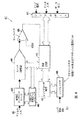
本明細書では、従来技術と比較して顕著な利点をもたらす入力レンジプログラム可能ADCについて説明する。本発明の一形態においては、この変換システムは、SAR ADCとして実装することができる。図1は、変換の前に、広レンジの双極性および単極性のアナログ入力信号を、減衰させるのに使用される従来式方法を示している。この例においては+2.5ボルトである、参照電圧Vrefが、バッファ102の入力に印加される。バッファリングされた参照電圧は、R1、R2、およびR3で形成される抵抗分圧器の上端に印加される。
図2に関してここで留意すべきことは、ADCのコンパレータおよびすべてのSAR論理は、5ボルトサブミクロンCMOS技術を用いて実施することができることである。アナログ入力スイッチだけが、±15ボルトCMOSデバイスを使用して製造する必要があり、このデバイスは、要求される高いゲート電圧に対処するために、より太いゲート酸化物を使用する。
すなわち、サンプリングされるアナログ入力電圧は次のようになる。

上記のように、図2は、2値重み付けキャパシタC7〜C0の集合と、コンパレータ204に対して最短距離に位置する「ダミー」キャパシタ(または終端キャパシタ)CDとからなる、容量性再分布DAC、またはCapDACを示している。CDの値は、LSBキャパシタC0のキャパシタンスと実質的に等しい。図2の回路において、終端キャパシタは、アナログ入力のサンプリングを行わず、オフセットを最小化するために、接地に維持される。図2の8ビットキャパシタ配列は、サンプルモードで示してある。配列の合計キャパシタンスは256Cであり、ここで、Cは図示された実装に対する、単位キャパシタンスである。
このように、この例においては、アナログ入力信号は、8分の1に減衰される。したがって、+10から−10ボルトまで変化する入力信号を仮定すると、コンパレータ204は、実際には±1.25ボルトを認識する。共通モード電圧Vcom203が1.25ボルトの場合には、入力信号は、コンパレータ204の共通モードレンジ範囲内に保持される。次いで、既知の逐次近似技法を使用して、入力信号をディジタル化することができる。
高電圧デバイス301、302は、アナログ入力信号を取り込み、それを直接、サンプリングキャパシタ303へと切り換える。勿論のこと、高電圧制御信号が、高電圧トランジスタ301、302のゲートに対して必要となるが、これらの制御信号は、5ボルトCMOSレベルからの簡単なレベルシフトによってもたらすことができる。
図4は、本発明による、全体を番号400で示す、プログラマブル入力電圧レンジ機能を組み込んだ、完成したSAR ADCシステムのブロック図である。CapDACの1つまたは2つ以上のキャパシタに、高電圧スイッチ402の配列を介して、アナログ入力信号401が流される。SAR論理406は、知られた方法で信号取得と変換の制御も行うが、これはまた、CapDAC配列のどのキャパシタに、入力信号をサンプリングするかを制御する。
図5は、レンジデコーダ論理の詳細図である。勿論のこと、いくつかの論理実装が、この応用を満足するであろう。図5の実装は単に、SAR ADCに対する適当な組のレンジを生成する1つの有効な方法である。SAR ADCのレンジを制御する3つの入力信号がある。これらは、極性ビット(Polarity Bit)501、レンジ1ビット(Range 1 bit)502、およびレンジ0ビット(Range 0 bit)503である。これらの信号のそれぞれは、インバータ504に流されて、信号およびその論理補数の両方が、デコーダセクションに対して利用可能にされる。
アナログ・ディジタル変換器の大多数は、時間軸のある点において、変換すべき信号は何らかの形態のメモリデバイスにサンプリングしなくてはならないという、原理に基づいて動作する。次いで、格納された信号は、既知の変換技法/アーキテクチャによってディジタル語に変換することができる。通常は(必須ではないが)、サンプリングされたアナログ信号を格納するためのメモリデバイスとしてキャパシタを使用する。
ここで、スイッチはすべて、本発明の先の態様について考察した、高電圧デバイスで構成されていると仮定する。広レンジ信号は、式(5)によって減衰させることができる。±10v信号に対しては、1×CHだけにサンプリング(すなわち、8で除算)。±5v信号に対しては、2×CH上だけにサンプリング(すなわち、4で除算)、以下同様である。
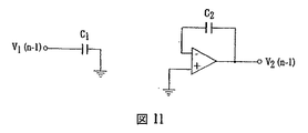
おそらく、シグマ・デルタ変換器の基本ビルディングブロックの最も重要なものは、図15のシグマ・デルタ変換器の合計1502部分および積分器1503部分を実現するスイッチドキャパシタ積分器である。図9は、概略図形式で、スイッチドキャパシタ積分器を示す。このスイッチドキャパシタ積分器は、アナログ入力電圧V1をサンプリングするのに使用される。
Claims (20)
- 単一基板上に製造される入力電圧レンジプログラム可能アナログ・ディジタル変換器集積回路デバイスであって、
標準サブミクロン低電圧CMOSプロセスを使用して製造されて、固有ダイナミックレンジを有する、アナログ・ディジタル変換器(ADC)サブシステム;
入力電圧が1つまたは2つ以上の選択されたサンプリングキャパシタにサンプリングされて、前記ADCの固有ダイナミックレンジに実質的に一致するように前記入力電圧がスケーリングされる、入力電圧スケーリングネットワーク;
より高いゲート電圧に対応するために分割ゲート酸化物プロセスを使用して製造される高電圧MOSサンプリングスイッチのネットワークであって、前記入力電圧が前記サンプリングキャパシタの1つまたは2つ以上に選択的にサンプリングされるように、前記入力電圧と前記入力電圧スケーリングネットワークの間に置かれている、前記高電圧サンプリングスイッチのネットワーク;および
前記高電圧サンプリングスイッチに低電圧の制御信号を結合するための、低電圧から高電圧へのレベルシフタのネットワーク、
を含む、前記入力電圧レンジプログラム可能アナログ・ディジタル変換器集積回路デバイス。 - 入力電圧スケーリングネットワークは、ADCにサンプリングされる入力電圧を供給する入力増幅器内に並列接続されたサンプリングキャパシタの配列を含む、請求項1に記載の入力電圧レンジプログラム可能アナログ・ディジタル変換器集積回路デバイス。
- サンプリングキャパシタは、アナログ入力電圧とサンプリングされる出力信号がそこから引き出される入力増幅器との間に置かれている、請求項2に記載の入力電圧レンジプログラム可能アナログ・ディジタル変換器集積回路デバイス。
- ADCはシグマ・デルタ変換器である、請求項3に記載の入力電圧レンジプログラム可能アナログ・ディジタル変換器集積回路デバイス。
- ADCはパイプライン変換器である、請求項3に記載の入力電圧レンジプログラム可能アナログ・ディジタル変換器集積回路デバイス。
- ADCは逐次近似変換器である、請求項3に記載の入力電圧レンジプログラム可能アナログ・ディジタル変換器集積回路デバイス。
- 入力電圧がそれにサンプリングされる入力電圧スケーリングネットワークの1つまたは2つ以上の要素を選択する、レンジデコーダ論理をさらに含む、請求項1に記載の入力電圧レンジプログラム可能アナログ・ディジタル変換器集積回路デバイス。
- 入力電圧レンジは双極性である、請求項7に記載の入力電圧レンジプログラム可能アナログ・ディジタル変換器集積回路デバイス。
- レンジデコーダ論理は、関連するレンジレジスタに書き込まれたレンジ選択制御語に応答する、請求項7に記載の入力電圧レンジプログラム可能アナログ・ディジタル変換器集積回路デバイス。
- レンジレジスタは、ディジタル通信インターフェイスを介してプログラム可能である、請求項9に記載の入力電圧レンジプログラム可能アナログ・ディジタル変換器集積回路デバイス。
- ディジタル通信インターフェイスは、シリアル通信インターフェイスである、請求項10に記載の入力電圧レンジプログラム可能アナログ・ディジタル変換器集積回路デバイス。
- シリアル通信インターフェイスは双方向性である、請求項11に記載の入力電圧レンジプログラム可能アナログ・ディジタル変換器集積回路デバイス。
- 単一基板上に製造される入力電圧レンジプログラム可能アナログ・ディジタル変換器集積回路デバイスであって、
標準サブミクロン低電圧CMOSプロセスを使用して製造されて、固有ダイナミックレンジを有する、アナログ・ディジタル変換器(ADC)サブシステム;
入力電圧が1つまたは2つ以上の選択されたサンプリングキャパシタにサンプリングされて、前記ADCの固有ダイナミックレンジに実質的に一致するように前記入力電圧がスケーリングされる、入力電圧スケーリングネットワーク;
より高いゲート電圧に対応するために分割ゲート酸化物プロセスを使用して製造される高電圧MOSサンプリングスイッチのネットワークであって、前記入力電圧が前記サンプリングキャパシタの1つまたは2つ以上に選択的にサンプリングされるように、前記入力電圧と前記入力電圧スケーリングネットワークの間に置かれた、前記高電圧サンプリングスイッチのネットワーク;
前記高電圧MOSサンプリングスイッチのネットワークを制御して、前記サンプリングキャパシタの前記1つまたは2つ以上を選択する、レンジデコーダ論理;
前記レンジデコーダ論理がそれに応答するレンジ選択制御語が、それに書き込まれるレンジレジスタ;および
前記高電圧サンプリングスイッチに低電圧の制御信号を結合するための、低電圧から高電圧へのレベルシフタのネットワーク、
を含む、前記入力電圧レンジプログラム可能アナログ・ディジタル変換器集積回路デバイス。 - ADCはシグマ・デルタ変換器である、請求項13に記載の入力電圧レンジプログラム可能アナログ・ディジタル変換器集積回路デバイス。
- ADCはパイプライン変換器である、請求項13に記載の入力電圧レンジプログラム可能アナログ・ディジタル変換器集積回路デバイス。
- ADCは逐次近似変換器である、請求項13に記載の入力電圧レンジプログラム可能アナログ・ディジタル変換器集積回路デバイス。
- レンジレジスタは、ディジタル通信インターフェイスを介してプログラム可能である、請求項13に記載の入力電圧レンジプログラム可能アナログ・ディジタル変換器集積回路デバイス。
- ディジタル通信インターフェイスは、シリアル通信インターフェイスである、請求項17に記載の入力電圧レンジプログラム可能アナログ・ディジタル変換器集積回路デバイス。
- シリアル通信インターフェイスは双方向性である、請求項18に記載の入力電圧レンジプログラム可能アナログ・ディジタル変換器集積回路デバイス。
- 入力電圧レンジは双極性である、請求項13に記載の入力電圧レンジプログラム可能アナログ・ディジタル変換器集積回路デバイス。
Applications Claiming Priority (3)
| Application Number | Priority Date | Filing Date | Title |
|---|---|---|---|
| US10/807,778 US6940445B2 (en) | 2002-12-27 | 2004-03-24 | Programmable input range ADC |
| US10/807,778 | 2004-03-24 | ||
| PCT/US2005/009680 WO2005096503A1 (en) | 2004-03-24 | 2005-03-24 | Programmable input range adc |
Publications (3)
| Publication Number | Publication Date |
|---|---|
| JP2007531408A JP2007531408A (ja) | 2007-11-01 |
| JP2007531408A5 JP2007531408A5 (ja) | 2007-12-27 |
| JP5236285B2 true JP5236285B2 (ja) | 2013-07-17 |
Family
ID=34965105
Family Applications (1)
| Application Number | Title | Priority Date | Filing Date |
|---|---|---|---|
| JP2007505136A Expired - Fee Related JP5236285B2 (ja) | 2004-03-24 | 2005-03-24 | プログラマブル入力レンジadc |
Country Status (5)
| Country | Link |
|---|---|
| US (2) | US6940445B2 (ja) |
| EP (1) | EP1728328A1 (ja) |
| JP (1) | JP5236285B2 (ja) |
| CN (1) | CN1934787B (ja) |
| WO (1) | WO2005096503A1 (ja) |
Families Citing this family (72)
| Publication number | Priority date | Publication date | Assignee | Title |
|---|---|---|---|---|
| WO2002019666A2 (en) | 2000-09-01 | 2002-03-07 | Nextlink.To A/S | A communications terminal, a system and a method for internet/network telephony |
| US8049573B2 (en) * | 2004-06-03 | 2011-11-01 | Silicon Laboratories Inc. | Bidirectional multiplexed RF isolator |
| US8169108B2 (en) * | 2004-06-03 | 2012-05-01 | Silicon Laboratories Inc. | Capacitive isolator |
| US7447492B2 (en) | 2004-06-03 | 2008-11-04 | Silicon Laboratories Inc. | On chip transformer isolator |
| US8198951B2 (en) | 2004-06-03 | 2012-06-12 | Silicon Laboratories Inc. | Capacitive isolation circuitry |
| US7421028B2 (en) | 2004-06-03 | 2008-09-02 | Silicon Laboratories Inc. | Transformer isolator for digital power supply |
| US7376212B2 (en) | 2004-06-03 | 2008-05-20 | Silicon Laboratories Inc. | RF isolator with differential input/output |
| US7821428B2 (en) | 2004-06-03 | 2010-10-26 | Silicon Laboratories Inc. | MCU with integrated voltage isolator and integrated galvanically isolated asynchronous serial data link |
| US7460604B2 (en) | 2004-06-03 | 2008-12-02 | Silicon Laboratories Inc. | RF isolator for isolating voltage sensing and gate drivers |
| US7902627B2 (en) | 2004-06-03 | 2011-03-08 | Silicon Laboratories Inc. | Capacitive isolation circuitry with improved common mode detector |
| US7577223B2 (en) | 2004-06-03 | 2009-08-18 | Silicon Laboratories Inc. | Multiplexed RF isolator circuit |
| US8441325B2 (en) | 2004-06-03 | 2013-05-14 | Silicon Laboratories Inc. | Isolator with complementary configurable memory |
| US7737871B2 (en) | 2004-06-03 | 2010-06-15 | Silicon Laboratories Inc. | MCU with integrated voltage isolator to provide a galvanic isolation between input and output |
| US7738568B2 (en) | 2004-06-03 | 2010-06-15 | Silicon Laboratories Inc. | Multiplexed RF isolator |
| US7302247B2 (en) | 2004-06-03 | 2007-11-27 | Silicon Laboratories Inc. | Spread spectrum isolator |
| US7015852B1 (en) * | 2004-11-30 | 2006-03-21 | Freescale Semiconductor, Inc. | Cyclic analog-to-digital converter |
| JP4803729B2 (ja) * | 2006-03-14 | 2011-10-26 | ルネサスエレクトロニクス株式会社 | 半導体集積回路 |
| DE102006015762B4 (de) * | 2006-04-04 | 2013-05-08 | Austriamicrosystems Ag | Analog/Digital-Wandleranordnung und Verfahren |
| DE102006025116B4 (de) * | 2006-05-30 | 2020-06-04 | Austriamicrosystems Ag | Einstellbare Analog-Digital-Wandleranordnung und Verfahren zur Analog-Digital-Wandlung |
| TWI328331B (en) * | 2006-07-21 | 2010-08-01 | Asustek Comp Inc | Level shifter |
| WO2008021241A2 (en) * | 2006-08-11 | 2008-02-21 | Entegris, Inc. | Auto ranging system and method for an analog signal |
| JP4837501B2 (ja) * | 2006-09-06 | 2011-12-14 | 浜松ホトニクス株式会社 | Ad変換回路および光検出装置 |
| US7511648B2 (en) * | 2007-04-23 | 2009-03-31 | Texas Instruments Incorporated | Integrating/SAR ADC and method with low integrator swing and low complexity |
| DE102007033689B4 (de) * | 2007-07-19 | 2009-03-19 | Texas Instruments Deutschland Gmbh | Analog-Digital-Wandler mit sukzessivem Approximationsregister und großem Eingangsbereich |
| US7782237B2 (en) * | 2008-06-13 | 2010-08-24 | The Board Of Trustees Of The Leland Stanford Junior University | Semiconductor sensor circuit arrangement |
| DE102008035215B4 (de) * | 2008-07-29 | 2010-09-09 | Texas Instruments Deutschland Gmbh | Elektronisches Bauelement und Verfahren zur Analog-Digital-Wandlung unter Verwendung von sukzessiver Approximation |
| US7868795B2 (en) | 2008-09-30 | 2011-01-11 | Freescale Semiconductor, Inc. | Data conversion circuitry with an extra successive approximation step and method therefor |
| US7880650B2 (en) * | 2008-09-30 | 2011-02-01 | Freescale Semiconductor, Inc. | Method and apparatus for testing data converter |
| US7868796B2 (en) * | 2008-09-30 | 2011-01-11 | Freescale Semiconductor, Inc. | Self-calibrating data conversion circuitry and method therefor |
| US7733258B2 (en) | 2008-09-30 | 2010-06-08 | Freescale Semiconductor, Inc. | Data conversion circuitry for converting analog signals to digital signals and vice-versa and method therefor |
| US7876254B2 (en) * | 2008-09-30 | 2011-01-25 | Freescale Semiconductor, Inc. | Data conversion circuitry having successive approximation circuitry and method therefor |
| US7821441B2 (en) * | 2008-12-19 | 2010-10-26 | Silicon Laboratories Inc. | SAR analog-to-digital converter having variable currents for low power mode of operation |
| DE102009004564B4 (de) * | 2009-01-14 | 2013-08-22 | Texas Instruments Deutschland Gmbh | ADC mit energiesparender Abtastung |
| JP2010166298A (ja) * | 2009-01-15 | 2010-07-29 | Fujitsu Ltd | アナログデジタル回路 |
| US8248280B2 (en) * | 2009-09-29 | 2012-08-21 | Silicon Laboratories Inc. | Successive approximation register (SAR) analog-to-digital converter (ADC) having optimized filter |
| US20110254569A1 (en) * | 2010-04-15 | 2011-10-20 | Peter Bogner | Measurement apparatus |
| EP2388923B1 (en) * | 2010-05-21 | 2013-12-04 | Stichting IMEC Nederland | Asynchronous digital slope analog-to-digital converter and method thereof |
| US8130133B2 (en) | 2010-07-27 | 2012-03-06 | Linear Technology Corporation | A/D converter using isolation switches |
| EP2421155B1 (en) * | 2010-08-02 | 2013-07-03 | Fraunhofer-Gesellschaft zur Förderung der Angewandten Forschung e.V. | A hybrid analog-to-digital converter, an image sensor and a method for providing a plurality of ditigal signals |
| US8451032B2 (en) | 2010-12-22 | 2013-05-28 | Silicon Laboratories Inc. | Capacitive isolator with schmitt trigger |
| US8378864B2 (en) * | 2011-03-16 | 2013-02-19 | Integrated Device Technology, Inc. | Apparatuses and methods for reducing errors in analog to digital converters |
| US8477052B2 (en) | 2011-04-05 | 2013-07-02 | Freescale Semiconductor, Inc. | Method and apparatus for self-test of successive approximation register (SAR) A/D converter |
| US9081038B2 (en) * | 2011-10-04 | 2015-07-14 | Analog Devices, Inc. | Voltage monitor |
| CN103138762B (zh) * | 2011-11-30 | 2016-04-27 | 禾瑞亚科技股份有限公司 | 多阶取样保持电路 |
| US8552897B1 (en) * | 2012-03-22 | 2013-10-08 | Analog Devices, Inc. | Reference circuit suitable for use with an analog to digital converter and an analog to digital converter including such a reference circuit |
| JP2013059105A (ja) * | 2012-11-19 | 2013-03-28 | Fujitsu Ltd | アナログデジタル回路及びそのアナログデジタル回路を用いた受信機 |
| JP6103934B2 (ja) * | 2012-12-28 | 2017-03-29 | キヤノン株式会社 | 光電変換装置、撮像システム、および光電変換装置の駆動方法 |
| JP6034699B2 (ja) | 2013-01-07 | 2016-11-30 | ルネサスエレクトロニクス株式会社 | 半導体装置及びそのコマンド制御方法 |
| CN103078641A (zh) * | 2013-01-17 | 2013-05-01 | 陕西北斗恒通信息科技有限公司 | 多通道抗干扰数字采样装置 |
| JP6313018B2 (ja) | 2013-11-13 | 2018-04-18 | ルネサスエレクトロニクス株式会社 | 設計支援装置、半導体装置及びコンパイルプログラム |
| US9231546B2 (en) | 2014-06-06 | 2016-01-05 | The Regents Of The University Of Michigan | Multi-dimensional array of impedance elements |
| CN104617955B (zh) * | 2015-01-19 | 2018-04-17 | 上海华虹宏力半导体制造有限公司 | Sar adc的采样保持电路 |
| US9722624B2 (en) | 2015-04-20 | 2017-08-01 | Samsung Electronics Co., Ltd | Semiconductor device comprising successive approximation register analog to digital converter with variable sampling capacitor |
| CN106571824A (zh) * | 2015-10-08 | 2017-04-19 | 联发科技(新加坡)私人有限公司 | 信号处理电路 |
| US11475269B2 (en) | 2015-12-15 | 2022-10-18 | Analog Devices, Inc. | Convolutional neural network |
| US9800262B1 (en) | 2016-09-07 | 2017-10-24 | Analog Devices Global | Precision low noise continuous time sigma delta converter |
| EP3293888B1 (en) | 2016-09-13 | 2020-08-26 | Allegro MicroSystems, LLC | Signal isolator having bidirectional communication between die |
| CN108990427B (zh) * | 2017-03-30 | 2023-02-21 | 深圳市汇顶科技股份有限公司 | 模数转换电路和方法 |
| US10404264B2 (en) | 2017-09-11 | 2019-09-03 | Analog Devices, Inc. | Method of performing analog-to-digital conversion |
| JP7102515B2 (ja) * | 2018-05-22 | 2022-07-19 | オリンパス株式会社 | デジタルアナログ変換器、アナログデジタル変換器、信号処理装置、固体撮像装置、および駆動方法 |
| US11265006B2 (en) | 2018-08-08 | 2022-03-01 | Infineon Technologies Ag | Using a sampling switch for multiple evaluation units |
| CN112585951B (zh) * | 2018-08-16 | 2023-11-14 | 索尼半导体解决方案公司 | 成像元件 |
| US10871757B2 (en) * | 2018-09-18 | 2020-12-22 | Texas Instruments Incorporated | Binary digital input module having comparator and isolated output |
| JP7176369B2 (ja) * | 2018-11-20 | 2022-11-22 | 株式会社デンソー | A/d変換器 |
| JP7102626B2 (ja) * | 2019-02-25 | 2022-07-19 | ヒタチ・エナジー・スウィツァーランド・アクチェンゲゼルシャフト | 電流および電圧測定のための方法ならびにデバイス |
| JP7249832B2 (ja) * | 2019-03-19 | 2023-03-31 | 株式会社東芝 | サンプルホールド回路、及びad変換器 |
| US10826520B1 (en) * | 2019-08-09 | 2020-11-03 | Texas Instruments Incorporated | Successive approximation register analog-to-digital converter |
| US11115244B2 (en) | 2019-09-17 | 2021-09-07 | Allegro Microsystems, Llc | Signal isolator with three state data transmission |
| KR102744050B1 (ko) | 2020-02-06 | 2024-12-17 | 삼성전자주식회사 | 아날로그 디지털 변환 장치 및 아날로그 디지털 변환 방법 |
| US10903843B1 (en) | 2020-02-14 | 2021-01-26 | Analog Devices International Unlimited Company | SAR ADC with variable sampling capacitor |
| US11418890B1 (en) * | 2021-04-15 | 2022-08-16 | Knowles Electronics, Llc | Digital sensors, electrical circuits and methods |
| CN113739829A (zh) * | 2021-08-19 | 2021-12-03 | 重庆物康科技有限公司 | 光纤光栅解调方法及解调系统 |
Family Cites Families (25)
| Publication number | Priority date | Publication date | Assignee | Title |
|---|---|---|---|---|
| US4348658A (en) | 1980-05-09 | 1982-09-07 | Motorola, Inc. | Analog-to-digital converter using half range technique |
| JPH0773207B2 (ja) * | 1984-05-11 | 1995-08-02 | セイコーエプソン株式会社 | 出力回路 |
| EP0211972A1 (en) * | 1985-08-07 | 1987-03-04 | Eaton Corporation | Raised gate efet |
| JPS6485416A (en) * | 1987-09-28 | 1989-03-30 | Nec Corp | Level shift circuit |
| JPH01176115A (ja) * | 1987-12-29 | 1989-07-12 | Nec Corp | 半導体集積回路 |
| JPH0310420A (ja) * | 1989-06-07 | 1991-01-18 | Nec Corp | アナログ・ディジタル変換器 |
| JP2896221B2 (ja) * | 1990-10-30 | 1999-05-31 | 株式会社東芝 | A/dコンバータ |
| US5784327A (en) * | 1991-06-12 | 1998-07-21 | Hazani; Emanuel | Memory cell array selection circuits |
| US5248974A (en) * | 1991-06-27 | 1993-09-28 | Texas Instruments Incorporated | Dielectric relaxation correction circuit for charge-redistribution a/d converters |
| US5235333A (en) * | 1992-03-05 | 1993-08-10 | Burr-Brown Corporation | Hysteresis-insensitive single-comparator successive approximation analog-to-digital converter |
| JPH07142979A (ja) * | 1993-11-15 | 1995-06-02 | Fujitsu Ltd | サンプル・ホールド回路 |
| US5694356A (en) | 1994-11-02 | 1997-12-02 | Invoice Technology, Inc. | High resolution analog storage EPROM and flash EPROM |
| US5684487A (en) | 1995-06-05 | 1997-11-04 | Analog Devices, Incorporated | A/D converter with charge-redistribution DAC and split summation of main and correcting DAC outputs |
| US6010929A (en) * | 1996-12-11 | 2000-01-04 | Texas Instruments Incorporated | Method for forming high voltage and low voltage transistors on the same substrate |
| US5861831A (en) | 1996-12-23 | 1999-01-19 | Analog Devices, Inc. | Intermediate frequency (IF) sampling clock-to-clock auto-ranging analog-to-digital converter (ADC) and method |
| JPH10303751A (ja) | 1997-04-22 | 1998-11-13 | Miyagi Oki Denki Kk | アナログ/ディジタル変換器 |
| TW351001B (en) * | 1997-05-03 | 1999-01-21 | United Microelectronics Corp | High-density transistor and the manufacturing method |
| JP2001517415A (ja) | 1998-01-20 | 2001-10-02 | マイクロチップ テクノロジー インコーポレイテッド | 連続近似レジスタ(sar)アナログ/デジタル(a/d)コンバータの低電圧動作のためのドライバ回路および方法 |
| EP0935195A2 (en) | 1998-02-06 | 1999-08-11 | Analog Devices, Inc. | "An integrated circuit with a high resolution analog-to-digital converter, a microcontroller and high density memory and an emulator for an integrated circuit |
| US6144331A (en) | 1998-04-08 | 2000-11-07 | Texas Instruments Incorporated | Analog to digital converter with a differential output resistor-digital-to-analog-converter for improved noise reduction |
| DE19936327C2 (de) | 1999-08-02 | 2003-04-24 | Infineon Technologies Ag | Verfahren und Vorrichtung zur Durchführung von ratiometrischen Messungen unter Verwendung eines Analog/Digital- oder eines Digital/Analog-Umsetzers, Analog/Digital- oder Digital/Analog-Umsetzer, und Verfahren zum Betreiben eines Analog/Digital- oder Digital/Analog-Umsetzers |
| US6456220B1 (en) | 2000-06-19 | 2002-09-24 | Cygnal Integrated Products, Inc. | Analog-to-digital converter for processing differential and single-ended inputs |
| US6388589B1 (en) | 2000-07-17 | 2002-05-14 | Trw Inc. | Programmable video interface |
| JP2002335151A (ja) * | 2001-05-10 | 2002-11-22 | Sharp Corp | 多電源出力バッファ |
| US6731232B1 (en) * | 2002-12-27 | 2004-05-04 | Analog Devices, Inc. | Programmable input range SAR ADC |
-
2004
- 2004-03-24 US US10/807,778 patent/US6940445B2/en not_active Expired - Fee Related
-
2005
- 2005-03-24 CN CN200580009253.4A patent/CN1934787B/zh not_active Expired - Fee Related
- 2005-03-24 EP EP05732937A patent/EP1728328A1/en not_active Withdrawn
- 2005-03-24 WO PCT/US2005/009680 patent/WO2005096503A1/en not_active Ceased
- 2005-03-24 JP JP2007505136A patent/JP5236285B2/ja not_active Expired - Fee Related
- 2005-09-01 US US11/219,551 patent/US20060001563A1/en not_active Abandoned
Also Published As
| Publication number | Publication date |
|---|---|
| CN1934787B (zh) | 2016-01-20 |
| WO2005096503A1 (en) | 2005-10-13 |
| US20060001563A1 (en) | 2006-01-05 |
| JP2007531408A (ja) | 2007-11-01 |
| CN1934787A (zh) | 2007-03-21 |
| EP1728328A1 (en) | 2006-12-06 |
| US6940445B2 (en) | 2005-09-06 |
| US20050151680A1 (en) | 2005-07-14 |
Similar Documents
| Publication | Publication Date | Title |
|---|---|---|
| JP5236285B2 (ja) | プログラマブル入力レンジadc | |
| CN1732624B (zh) | 可编程输入范围sar adc | |
| CN1526202B (zh) | 具有单端输入的高速、高分辨率和低功耗的模/数转换器 | |
| Wei et al. | An 8-b 400-MS/s 2-b-per-cycle SAR ADC with resistive DAC | |
| CN108574487A (zh) | 具有基于分裂电容器的数模转换器的逐次逼近寄存器模数转换器 | |
| JPH06152420A (ja) | アナログ/ディジタル変換器 | |
| WO2003001675A2 (en) | Nmulti-level quantizer with dithering and multi-threshold generation for a multi-bt sigma-delta modulator | |
| US6130635A (en) | Method of converting an analog signal in an A/D converter utilizing RDAC precharging | |
| US9742423B1 (en) | Separating most significant bits and least significant bits in charge storage elements of an analog-to-digital converter | |
| JPH0734541B2 (ja) | 逐次比較形アナログ・ディジタル変換方式 | |
| JPS6211817B2 (ja) | ||
| US9831889B1 (en) | Converting large input analog signals in an analog-to-digital converter without input attenuation | |
| TWI661681B (zh) | 類比至數位轉換器及可適用於類比至數位轉換器的介面電路 | |
| US5719576A (en) | Capacitor array digital/analog converter with compensation array for stray capacitance | |
| Kleinfelder | Development of a switched capacitor based multi-channel transient waveform recording integrated circuit | |
| US20050057283A1 (en) | Sample and hold circuit based on an ultra linear switch | |
| JP2004032089A (ja) | Ad変換器 | |
| CN115085733B (zh) | 具备暂停转换功能的模数转换器装置以及其操作方法 | |
| US6198313B1 (en) | Infinite sample-and-hold circuit | |
| US7403148B2 (en) | Methods and apparatus to balance reference settling in switched-capacitor pipelined digital to analog converter | |
| Campos et al. | A low-power 10-bit 0.01-to-12-MS/s asynchronous SAR ADC in 65-nm CMOS | |
| US7403150B1 (en) | Analog-to-digital converter architecture using a capacitor array structure | |
| Wang et al. | High speed CMOS digital-to-analog converter with linear interpolator | |
| JPS649774B2 (ja) | ||
| Louërat et al. | scalable SAR ADC |
Legal Events
| Date | Code | Title | Description |
|---|---|---|---|
| A521 | Request for written amendment filed |
Free format text: JAPANESE INTERMEDIATE CODE: A523 Effective date: 20071109 |
|
| A621 | Written request for application examination |
Free format text: JAPANESE INTERMEDIATE CODE: A621 Effective date: 20071109 |
|
| A977 | Report on retrieval |
Free format text: JAPANESE INTERMEDIATE CODE: A971007 Effective date: 20101014 |
|
| A131 | Notification of reasons for refusal |
Free format text: JAPANESE INTERMEDIATE CODE: A131 Effective date: 20101026 |
|
| A601 | Written request for extension of time |
Free format text: JAPANESE INTERMEDIATE CODE: A601 Effective date: 20110126 |
|
| A602 | Written permission of extension of time |
Free format text: JAPANESE INTERMEDIATE CODE: A602 Effective date: 20110202 |
|
| A601 | Written request for extension of time |
Free format text: JAPANESE INTERMEDIATE CODE: A601 Effective date: 20110228 |
|
| A602 | Written permission of extension of time |
Free format text: JAPANESE INTERMEDIATE CODE: A602 Effective date: 20110307 |
|
| A601 | Written request for extension of time |
Free format text: JAPANESE INTERMEDIATE CODE: A601 Effective date: 20110328 |
|
| A602 | Written permission of extension of time |
Free format text: JAPANESE INTERMEDIATE CODE: A602 Effective date: 20110404 |
|
| A521 | Request for written amendment filed |
Free format text: JAPANESE INTERMEDIATE CODE: A523 Effective date: 20110426 |
|
| A02 | Decision of refusal |
Free format text: JAPANESE INTERMEDIATE CODE: A02 Effective date: 20110531 |
|
| A521 | Request for written amendment filed |
Free format text: JAPANESE INTERMEDIATE CODE: A523 Effective date: 20110930 |
|
| A911 | Transfer to examiner for re-examination before appeal (zenchi) |
Free format text: JAPANESE INTERMEDIATE CODE: A911 Effective date: 20111124 |
|
| A912 | Re-examination (zenchi) completed and case transferred to appeal board |
Free format text: JAPANESE INTERMEDIATE CODE: A912 Effective date: 20120106 |
|
| A601 | Written request for extension of time |
Free format text: JAPANESE INTERMEDIATE CODE: A601 Effective date: 20120905 |
|
| A602 | Written permission of extension of time |
Free format text: JAPANESE INTERMEDIATE CODE: A602 Effective date: 20120911 |
|
| A601 | Written request for extension of time |
Free format text: JAPANESE INTERMEDIATE CODE: A601 Effective date: 20121003 |
|
| A602 | Written permission of extension of time |
Free format text: JAPANESE INTERMEDIATE CODE: A602 Effective date: 20121009 |
|
| A61 | First payment of annual fees (during grant procedure) |
Free format text: JAPANESE INTERMEDIATE CODE: A61 Effective date: 20130327 |
|
| R150 | Certificate of patent or registration of utility model |
Free format text: JAPANESE INTERMEDIATE CODE: R150 Ref document number: 5236285 Country of ref document: JP Free format text: JAPANESE INTERMEDIATE CODE: R150 |
|
| FPAY | Renewal fee payment (event date is renewal date of database) |
Free format text: PAYMENT UNTIL: 20160405 Year of fee payment: 3 |
|
| R250 | Receipt of annual fees |
Free format text: JAPANESE INTERMEDIATE CODE: R250 |
|
| R250 | Receipt of annual fees |
Free format text: JAPANESE INTERMEDIATE CODE: R250 |
|
| R250 | Receipt of annual fees |
Free format text: JAPANESE INTERMEDIATE CODE: R250 |
|
| R250 | Receipt of annual fees |
Free format text: JAPANESE INTERMEDIATE CODE: R250 |
|
| R250 | Receipt of annual fees |
Free format text: JAPANESE INTERMEDIATE CODE: R250 |
|
| R250 | Receipt of annual fees |
Free format text: JAPANESE INTERMEDIATE CODE: R250 |
|
| LAPS | Cancellation because of no payment of annual fees |