JP5240190B2 - 位相差板の製造方法 - Google Patents
位相差板の製造方法 Download PDFInfo
- Publication number
- JP5240190B2 JP5240190B2 JP2009509341A JP2009509341A JP5240190B2 JP 5240190 B2 JP5240190 B2 JP 5240190B2 JP 2009509341 A JP2009509341 A JP 2009509341A JP 2009509341 A JP2009509341 A JP 2009509341A JP 5240190 B2 JP5240190 B2 JP 5240190B2
- Authority
- JP
- Japan
- Prior art keywords
- laser
- plate
- retardation
- glass plate
- glass
- Prior art date
- Legal status (The legal status is an assumption and is not a legal conclusion. Google has not performed a legal analysis and makes no representation as to the accuracy of the status listed.)
- Expired - Fee Related
Links
Images



Classifications
-
- G—PHYSICS
- G02—OPTICS
- G02B—OPTICAL ELEMENTS, SYSTEMS OR APPARATUS
- G02B5/00—Optical elements other than lenses
- G02B5/30—Polarising elements
-
- G—PHYSICS
- G02—OPTICS
- G02B—OPTICAL ELEMENTS, SYSTEMS OR APPARATUS
- G02B5/00—Optical elements other than lenses
- G02B5/30—Polarising elements
- G02B5/3083—Birefringent or phase retarding elements
-
- C—CHEMISTRY; METALLURGY
- C03—GLASS; MINERAL OR SLAG WOOL
- C03C—CHEMICAL COMPOSITION OF GLASSES, GLAZES OR VITREOUS ENAMELS; SURFACE TREATMENT OF GLASS; SURFACE TREATMENT OF FIBRES OR FILAMENTS MADE FROM GLASS, MINERALS OR SLAGS; JOINING GLASS TO GLASS OR OTHER MATERIALS
- C03C23/00—Other surface treatment of glass not in the form of fibres or filaments
- C03C23/0005—Other surface treatment of glass not in the form of fibres or filaments by irradiation
- C03C23/0025—Other surface treatment of glass not in the form of fibres or filaments by irradiation by a laser beam
-
- G—PHYSICS
- G11—INFORMATION STORAGE
- G11B—INFORMATION STORAGE BASED ON RELATIVE MOVEMENT BETWEEN RECORD CARRIER AND TRANSDUCER
- G11B7/00—Recording or reproducing by optical means, e.g. recording using a thermal beam of optical radiation by modifying optical properties or the physical structure, reproducing using an optical beam at lower power by sensing optical properties; Record carriers therefor
- G11B7/004—Recording, reproducing or erasing methods; Read, write or erase circuits therefor
- G11B7/0065—Recording, reproducing or erasing by using optical interference patterns, e.g. holograms
-
- G—PHYSICS
- G11—INFORMATION STORAGE
- G11B—INFORMATION STORAGE BASED ON RELATIVE MOVEMENT BETWEEN RECORD CARRIER AND TRANSDUCER
- G11B7/00—Recording or reproducing by optical means, e.g. recording using a thermal beam of optical radiation by modifying optical properties or the physical structure, reproducing using an optical beam at lower power by sensing optical properties; Record carriers therefor
- G11B7/12—Heads, e.g. forming of the optical beam spot or modulation of the optical beam
- G11B7/135—Means for guiding the beam from the source to the record carrier or from the record carrier to the detector
- G11B7/1353—Diffractive elements, e.g. holograms or gratings
-
- G—PHYSICS
- G11—INFORMATION STORAGE
- G11B—INFORMATION STORAGE BASED ON RELATIVE MOVEMENT BETWEEN RECORD CARRIER AND TRANSDUCER
- G11B7/00—Recording or reproducing by optical means, e.g. recording using a thermal beam of optical radiation by modifying optical properties or the physical structure, reproducing using an optical beam at lower power by sensing optical properties; Record carriers therefor
- G11B7/12—Heads, e.g. forming of the optical beam spot or modulation of the optical beam
- G11B7/135—Means for guiding the beam from the source to the record carrier or from the record carrier to the detector
- G11B7/1365—Separate or integrated refractive elements, e.g. wave plates
Landscapes
- Physics & Mathematics (AREA)
- Optics & Photonics (AREA)
- Chemical & Material Sciences (AREA)
- General Physics & Mathematics (AREA)
- Health & Medical Sciences (AREA)
- Life Sciences & Earth Sciences (AREA)
- Toxicology (AREA)
- Engineering & Computer Science (AREA)
- Chemical Kinetics & Catalysis (AREA)
- General Chemical & Material Sciences (AREA)
- Geochemistry & Mineralogy (AREA)
- Materials Engineering (AREA)
- Organic Chemistry (AREA)
- Polarising Elements (AREA)
- Optical Head (AREA)
Description
2:レーザ光
3:レンズ
4:レーザ光走査領域
5:ビーム分岐素子
10:レーザ光走査領域周囲の複屈折領域
11:円筒レンズ(シリンドリカルレンズ)
12:ラインビーム
または、銅イオンや鉄イオンを含有させたガラスにレーザ照射し、リタデーション値が1/4波長になるように作製したものの両面に水晶複屈折板を積層することによっても作製できる。
厚さ1mmのソーダライムガラス板にパルスYAGレーザの3倍波(波長355nm、パルス幅25ns)を約φ1μmに集光照射し、走査速度5mm/sで、集光レンズはNA0.42の対物レンズを用い、ガラス板表面から200μm内部に焦点を結んだ状態で、ガラス板を直線状に走査して複屈折を誘起した。その後に、先程照射した部分の上部100μmに焦点を結んだ状態で、前述と同一条件でYAG3倍波レーザを照射した。使用したYAGレーザはコヒーレント社製AVIA−Xで、平均出力1W、繰り返し周波数80KHzで使用した。王子計測機器社製複屈折計(KOBRA−CCD)を用いて、レーザ照射部のリタデーションを波長540nmの入射光で測定すると、レーザ照射部に沿って幅約100μmの領域に約100nmのリタデーションが誘起できたことを確認した。またクロスニコル観察より、その主軸(異方性軸)の方向はガラス板の走査方向と同一方向であることが確認された。
厚さ3mmのソーダライムガラス板表面にCW発振している炭酸ガスレーザ(波長10.6μm)を焦点距離100mmのレンズでφ300μmのスポットに集光照射し、走査速度8mm/sでガラス板を直線状に走査し複屈折を誘起した。レーザの平均出力を2Wから0.5Wずつ増やしていき照射部のリタデーションをセナルモン法で測定した。その結果、レーザ出力と共にリタデーション値が増加し、3.5Wで照射した時に最大108nmのリタデーション値を得た。照射パワー密度×照射径通過時間とリタデーションの関係を図5に示す。
例2と同様に、CW発振している炭酸ガスレーザを平均出力4W以上で照射すると、ガラス板に割れが発生した。この時の照射パワー密度×照射径通過時間は、212.3J/cm2であった。
厚さ3mmのソーダライムガラス内部にパルスYAGレーザの3倍波(波長355nm、パルス幅25ns)をNA0.42の対物レンズで集光照射し、レーザ出力2W、繰返し周波数80KHz、走査速度10mm/sで直線的に走査して複屈折を誘起した。レーザ光を厚さ方向に100μm間隔で照射(積層)したものを作製し、積層数とリタデーション値の関係を測定した。その結果、積層数とリタデーション値の間に比例の関係があり、積層数を増やす事でリタデーション値の増加が可能でλ/2板も作製可能な事が分る。積層数とリタデーション値の間の関係を図7に示す。
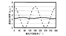
厚さ3mmのソーダライムガラス内部にパルスYAGレーザの3倍波(波長355nm、パルス幅25ns)をNA0.42の対物レンズで集光照射し、レーザ出力2W、繰返し周波数80KHz、走査速度10mm/sで直線的に走査して複屈折を誘起した。レーザ光を同一深さ位置内で3mm走査することを40μm間隔で100回実施したものを、深さ方向に100μm間隔で4回実施した。その結果、3mm×3mmの領域に116nmのリタデーションが均一に誘起できた。このようにして作製された位相差板に、該位相差板の主軸方向に対して同一方向と45度傾いた波長488nmの直線偏光を入射させ、出射部に偏光子を配し透過光強度を、偏光子を回転させモニターした。その結果を図8に示す。
なお、2007年4月9日に出願された日本特許出願2007−101982号に記載の明細書、特許請求の範囲、図面及び要約書の全内容をここに引用し、本発明の明細書の開示として、取り入れるものである。
Claims (1)
- レーザ光をレンズ、または凹面鏡によりガラス板内部または表面に焦点を結ぶよう集光照射し、ガラス板またはレーザ光を走査することで複屈折領域を形成し、一軸性複屈折を誘起する位相差板の製造方法であって、
前記レーザ光は、波長が190〜1100nm、パルス幅が1ns以上10ms以下、繰り返し周波数がfのレーザ光であり、
前記ガラス板は厚さは、0.1mm以上、5mm以下であり、
前記ガラス板への照射フルエンスをF(J/cm 2 )、レーザ集光径をd(cm)、走査速度をs(cm/s)として、照射フルエンスFと前記レーザ集光径内のレーザ照射回数d・f/sとの積であるF・d・f/sが、2000J/cm 2 以上、76000J/cm 2 以下であることを特徴とする位相差板の製造方法。
Priority Applications (1)
| Application Number | Priority Date | Filing Date | Title |
|---|---|---|---|
| JP2009509341A JP5240190B2 (ja) | 2007-04-09 | 2008-04-07 | 位相差板の製造方法 |
Applications Claiming Priority (4)
| Application Number | Priority Date | Filing Date | Title |
|---|---|---|---|
| JP2007101982 | 2007-04-09 | ||
| JP2007101982 | 2007-04-09 | ||
| PCT/JP2008/056895 WO2008126828A1 (ja) | 2007-04-09 | 2008-04-07 | 位相差板およびその製造方法 |
| JP2009509341A JP5240190B2 (ja) | 2007-04-09 | 2008-04-07 | 位相差板の製造方法 |
Publications (2)
| Publication Number | Publication Date |
|---|---|
| JPWO2008126828A1 JPWO2008126828A1 (ja) | 2010-07-22 |
| JP5240190B2 true JP5240190B2 (ja) | 2013-07-17 |
Family
ID=39863925
Family Applications (1)
| Application Number | Title | Priority Date | Filing Date |
|---|---|---|---|
| JP2009509341A Expired - Fee Related JP5240190B2 (ja) | 2007-04-09 | 2008-04-07 | 位相差板の製造方法 |
Country Status (7)
| Country | Link |
|---|---|
| US (2) | US8059337B2 (ja) |
| EP (1) | EP2136224A4 (ja) |
| JP (1) | JP5240190B2 (ja) |
| KR (1) | KR20100014893A (ja) |
| CN (1) | CN101652685B (ja) |
| TW (1) | TW200900760A (ja) |
| WO (1) | WO2008126828A1 (ja) |
Families Citing this family (16)
| Publication number | Priority date | Publication date | Assignee | Title |
|---|---|---|---|---|
| US7633033B2 (en) | 2004-01-09 | 2009-12-15 | General Lasertronics Corporation | Color sensing for laser decoating |
| US8536483B2 (en) * | 2007-03-22 | 2013-09-17 | General Lasertronics Corporation | Methods for stripping and modifying surfaces with laser-induced ablation |
| JP5136431B2 (ja) * | 2009-01-15 | 2013-02-06 | 株式会社デンソー | 半導体装置の製造方法 |
| JP2010243850A (ja) * | 2009-04-07 | 2010-10-28 | Fujifilm Corp | 多層複屈折バターン作製材料、及び多層複屈折パターンを有する物品の製造方法 |
| JP5455706B2 (ja) * | 2010-02-25 | 2014-03-26 | キヤノン株式会社 | 固体撮像装置、撮像ユニット及び撮像装置 |
| US10112257B1 (en) * | 2010-07-09 | 2018-10-30 | General Lasertronics Corporation | Coating ablating apparatus with coating removal detection |
| JP2013224974A (ja) * | 2010-08-20 | 2013-10-31 | Asahi Glass Co Ltd | 位相差板の製造方法および位相差板 |
| JPWO2012099078A1 (ja) * | 2011-01-20 | 2014-06-30 | 旭硝子株式会社 | 位相差板及び位相差板の製造方法 |
| WO2013123973A1 (en) | 2012-02-21 | 2013-08-29 | Carl Zeiss Sms Ltd. | Method and apparatus for compensating at least one defect of an optical system |
| US9895771B2 (en) | 2012-02-28 | 2018-02-20 | General Lasertronics Corporation | Laser ablation for the environmentally beneficial removal of surface coatings |
| FR3006068B1 (fr) * | 2013-05-24 | 2015-04-24 | Saint Gobain | Procede d'obtention d'un substrat |
| JP2015014740A (ja) * | 2013-07-08 | 2015-01-22 | 日本電気硝子株式会社 | 光学素子及びその製造方法 |
| US10086597B2 (en) | 2014-01-21 | 2018-10-02 | General Lasertronics Corporation | Laser film debonding method |
| CN105336759B (zh) | 2014-08-06 | 2018-06-29 | 上海和辉光电有限公司 | 显示面板 |
| US11314007B2 (en) | 2017-07-10 | 2022-04-26 | Lg Chem, Ltd. | Circularly polarizing plate |
| US20230286082A1 (en) * | 2022-03-11 | 2023-09-14 | Ats Industrial Automation Inc. | Laser cleaning of oxidized parts |
Citations (6)
| Publication number | Priority date | Publication date | Assignee | Title |
|---|---|---|---|---|
| JP2004145327A (ja) * | 2002-10-04 | 2004-05-20 | Dainippon Printing Co Ltd | 光学素子およびそれを用いた液晶表示装置 |
| JP2004252027A (ja) * | 2003-02-19 | 2004-09-09 | Citizen Watch Co Ltd | 液晶装置製造方法と液晶装置 |
| JP2007034139A (ja) * | 2005-07-29 | 2007-02-08 | Enplas Corp | 光学素子およびその製造方法 |
| JP2007086556A (ja) * | 2005-09-26 | 2007-04-05 | Okamoto Glass Co Ltd | 異方性ガラスの製造方法、異方性ガラス及び、これを用いた偏光素子 |
| JP2007212805A (ja) * | 2006-02-10 | 2007-08-23 | Central Glass Co Ltd | 複屈折性の光学素子およびその製造方法 |
| JP2007238342A (ja) * | 2006-03-06 | 2007-09-20 | Okamoto Glass Co Ltd | 複屈折を付与されたガラス材料の製造方法及び、その方法によって製造されるガラス材料 |
Family Cites Families (21)
| Publication number | Priority date | Publication date | Assignee | Title |
|---|---|---|---|---|
| US3689264A (en) * | 1970-03-19 | 1972-09-05 | Bell Telephone Labor Inc | Method for increasing index of refraction in transparent bodies and its application to light guides and the like |
| DE3720028A1 (de) * | 1987-06-16 | 1988-12-29 | Philips Patentverwaltung | Verfahren zur herstellung von lichtleitfasern |
| JPH08278410A (ja) | 1995-04-10 | 1996-10-22 | Sumitomo Chem Co Ltd | 光学異方体フィルムとその製造方法および液晶表示装置 |
| TW327208B (en) * | 1994-11-10 | 1998-02-21 | Sumitomo Chemical Co | Optically anisotropic film and process for producing the same and liquid crystal display device |
| JP3610403B2 (ja) | 1994-11-10 | 2005-01-12 | 住友化学株式会社 | 光学異方体フィルムとその製造方法および液晶表示装置 |
| US5761111A (en) * | 1996-03-15 | 1998-06-02 | President And Fellows Of Harvard College | Method and apparatus providing 2-D/3-D optical information storage and retrieval in transparent materials |
| JP3649835B2 (ja) * | 1996-03-18 | 2005-05-18 | 独立行政法人科学技術振興機構 | 光導波路の作製方法 |
| JP3461680B2 (ja) * | 1997-03-13 | 2003-10-27 | シャープ株式会社 | 光学素子の製造方法および画像表示装置 |
| US6392683B1 (en) * | 1997-09-26 | 2002-05-21 | Sumitomo Heavy Industries, Ltd. | Method for making marks in a transparent material by using a laser |
| JP3349422B2 (ja) * | 1998-02-12 | 2002-11-25 | 科学技術振興事業団 | 光導波路アレイ及びその製造方法 |
| US6573026B1 (en) * | 1999-07-29 | 2003-06-03 | Corning Incorporated | Femtosecond laser writing of glass, including borosilicate, sulfide, and lead glasses |
| JP4163825B2 (ja) | 1999-09-22 | 2008-10-08 | 富士フイルム株式会社 | 位相差板の製造方法 |
| US6796148B1 (en) * | 1999-09-30 | 2004-09-28 | Corning Incorporated | Deep UV laser internally induced densification in silica glasses |
| US6812983B2 (en) * | 2000-05-17 | 2004-11-02 | Fuji Photo Film Co., Ltd. | Retardation plate and fabrication method thereof, and plate for circularly polarizing light, ½ wave plate and reflection-type liquid crystal display device utilizing the retardation plate |
| US7568365B2 (en) * | 2001-05-04 | 2009-08-04 | President & Fellows Of Harvard College | Method and apparatus for micromachining bulk transparent materials using localized heating by nonlinearly absorbed laser radiation, and devices fabricated thereby |
| CA2396831A1 (en) * | 2002-08-02 | 2004-02-02 | Femtonics Corporation | Microstructuring optical wave guide devices with femtosecond optical pulses |
| US7486705B2 (en) * | 2004-03-31 | 2009-02-03 | Imra America, Inc. | Femtosecond laser processing system with process parameters, controls and feedback |
| US7586059B2 (en) * | 2004-08-27 | 2009-09-08 | Infineon Technologies Ag | Lithography mask substrate labeling system |
| TWI395978B (zh) * | 2004-12-03 | 2013-05-11 | Ohara Kk | 光學元件與製造光學元件的方法 |
| US7589039B2 (en) * | 2004-12-29 | 2009-09-15 | Corning Incorporated | Synthetic silica having low polarization-induced birefringence, method of making same and lithographic device comprising same |
| JP2007101982A (ja) | 2005-10-06 | 2007-04-19 | Konica Minolta Medical & Graphic Inc | 現像処理装置、現像処理方法及び画像記録装置 |
-
2008
- 2008-04-07 JP JP2009509341A patent/JP5240190B2/ja not_active Expired - Fee Related
- 2008-04-07 WO PCT/JP2008/056895 patent/WO2008126828A1/ja not_active Ceased
- 2008-04-07 CN CN2008800113197A patent/CN101652685B/zh not_active Expired - Fee Related
- 2008-04-07 KR KR1020097018317A patent/KR20100014893A/ko not_active Withdrawn
- 2008-04-07 EP EP08739998A patent/EP2136224A4/en not_active Withdrawn
- 2008-04-09 TW TW097112849A patent/TW200900760A/zh unknown
-
2009
- 2009-10-07 US US12/588,199 patent/US8059337B2/en not_active Expired - Fee Related
-
2011
- 2011-06-10 US US13/158,127 patent/US20110252834A1/en not_active Abandoned
Patent Citations (6)
| Publication number | Priority date | Publication date | Assignee | Title |
|---|---|---|---|---|
| JP2004145327A (ja) * | 2002-10-04 | 2004-05-20 | Dainippon Printing Co Ltd | 光学素子およびそれを用いた液晶表示装置 |
| JP2004252027A (ja) * | 2003-02-19 | 2004-09-09 | Citizen Watch Co Ltd | 液晶装置製造方法と液晶装置 |
| JP2007034139A (ja) * | 2005-07-29 | 2007-02-08 | Enplas Corp | 光学素子およびその製造方法 |
| JP2007086556A (ja) * | 2005-09-26 | 2007-04-05 | Okamoto Glass Co Ltd | 異方性ガラスの製造方法、異方性ガラス及び、これを用いた偏光素子 |
| JP2007212805A (ja) * | 2006-02-10 | 2007-08-23 | Central Glass Co Ltd | 複屈折性の光学素子およびその製造方法 |
| JP2007238342A (ja) * | 2006-03-06 | 2007-09-20 | Okamoto Glass Co Ltd | 複屈折を付与されたガラス材料の製造方法及び、その方法によって製造されるガラス材料 |
Also Published As
| Publication number | Publication date |
|---|---|
| US20100033817A1 (en) | 2010-02-11 |
| US8059337B2 (en) | 2011-11-15 |
| JPWO2008126828A1 (ja) | 2010-07-22 |
| TW200900760A (en) | 2009-01-01 |
| EP2136224A1 (en) | 2009-12-23 |
| KR20100014893A (ko) | 2010-02-11 |
| US20110252834A1 (en) | 2011-10-20 |
| WO2008126828A1 (ja) | 2008-10-23 |
| CN101652685B (zh) | 2012-07-04 |
| CN101652685A (zh) | 2010-02-17 |
| EP2136224A4 (en) | 2011-05-25 |
Similar Documents
| Publication | Publication Date | Title |
|---|---|---|
| JPWO2008126828A1 (ja) | 位相差板およびその製造方法 | |
| JP5902389B2 (ja) | 耐性を有し、無機的で、吸収性を有する紫外線グリッド偏光素子 | |
| Drevinskas et al. | High-performance geometric phase elements in silica glass | |
| JP5580826B2 (ja) | レーザ加工装置及びレーザ加工方法 | |
| KR101325520B1 (ko) | 레이저 어닐링 방법 및 레이저 어닐링 장치 | |
| Poole et al. | Liquid crystal films as on-demand, variable thickness (50–5000 nm) targets for intense lasers | |
| US8451536B2 (en) | Irradiation apparatus and manufacturing method for semiconductor device | |
| JP5998968B2 (ja) | ガラス基板の切断方法、ガラス基板及び近赤外線カットフィルタガラス | |
| US7256937B2 (en) | Structured polarizer and method for making the same | |
| Karimbana-Kandy et al. | Optimization of the thickness dependent third order optical nonlinearities of 2D Bi2Se3 layers | |
| JP2012015463A (ja) | Yagレーザアニーリング装置及びyagレーザ光によるアニーリング方法 | |
| Lee et al. | CMOS-compatible Si metasurface at visible wavelengths prepared by low-temperature green laser annealing | |
| JP4761992B2 (ja) | 複屈折性の光学素子を有する撮像機およびその光学素子の製造方法 | |
| RU2540727C1 (ru) | Способ формирования массива микрооптических элементов | |
| RU2554595C1 (ru) | Способ изготовления микрооптического растра | |
| Nakata et al. | Interfering ultraviolet femtosecond laser processing of gold thin film and prospect of shortest period | |
| JP5113998B2 (ja) | 異方性ガラスの製造方法、異方性ガラス及び、これを用いた偏光素子 | |
| JP2007238342A (ja) | 複屈折を付与されたガラス材料の製造方法及び、その方法によって製造されるガラス材料 | |
| CN106158576A (zh) | 一种利用玻璃掺杂钆靶获得高光谱纯度极紫外光源的方法 | |
| WO2012023429A1 (ja) | 位相差板の製造方法および位相差板 | |
| JP6631295B2 (ja) | 紫外線用フィルタ層、紫外線用フィルタ層の形成方法、紫外線用フィルタ、グリッド偏光素子及び偏光光照射装置 | |
| JPS5997105A (ja) | 干渉型偏光子 | |
| Paipulas et al. | Volume Bragg Grating Formation in Fused Silica with High Repetition Rate Femtosecond Yb: KGW Laser Pulses. | |
| US20230235446A1 (en) | Method for further improving laser pulsed deposition efficiency | |
| JP2006278274A (ja) | 複合酸化物薄膜及びその製造方法及び光学素子 |
Legal Events
| Date | Code | Title | Description |
|---|---|---|---|
| A621 | Written request for application examination |
Free format text: JAPANESE INTERMEDIATE CODE: A621 Effective date: 20110215 |
|
| A131 | Notification of reasons for refusal |
Free format text: JAPANESE INTERMEDIATE CODE: A131 Effective date: 20121113 |
|
| A521 | Request for written amendment filed |
Free format text: JAPANESE INTERMEDIATE CODE: A523 Effective date: 20121221 |
|
| TRDD | Decision of grant or rejection written | ||
| A01 | Written decision to grant a patent or to grant a registration (utility model) |
Free format text: JAPANESE INTERMEDIATE CODE: A01 Effective date: 20130305 |
|
| A61 | First payment of annual fees (during grant procedure) |
Free format text: JAPANESE INTERMEDIATE CODE: A61 Effective date: 20130318 |
|
| FPAY | Renewal fee payment (event date is renewal date of database) |
Free format text: PAYMENT UNTIL: 20160412 Year of fee payment: 3 |
|
| FPAY | Renewal fee payment (event date is renewal date of database) |
Free format text: PAYMENT UNTIL: 20160412 Year of fee payment: 3 |
|
| LAPS | Cancellation because of no payment of annual fees |