JP5373331B2 - 基板処理装置 - Google Patents
基板処理装置 Download PDFInfo
- Publication number
- JP5373331B2 JP5373331B2 JP2008195053A JP2008195053A JP5373331B2 JP 5373331 B2 JP5373331 B2 JP 5373331B2 JP 2008195053 A JP2008195053 A JP 2008195053A JP 2008195053 A JP2008195053 A JP 2008195053A JP 5373331 B2 JP5373331 B2 JP 5373331B2
- Authority
- JP
- Japan
- Prior art keywords
- substrate
- processing
- panel
- negative pressure
- panel substrate
- Prior art date
- Legal status (The legal status is an assumption and is not a legal conclusion. Google has not performed a legal analysis and makes no representation as to the accuracy of the status listed.)
- Expired - Fee Related
Links
Images





Landscapes
- Liquid Crystal (AREA)
- Devices For Indicating Variable Information By Combining Individual Elements (AREA)
Description
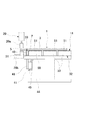
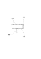
3 上基板 4 IC回路素子
5 ACF 10 搬入部
11 ACF貼り付けステージ 12 IC回路素子供給・仮圧着ステージ
13 本圧着ステージ 20 ACF貼り付けユニット
21 仮圧着ユニット 22 圧着ユニット
30 基板ピッチ送り駆動部 31 基板支持部
32 基板フローティング部 40 可動ビーム
41 駆動部材 42 吸着孔
43 負圧配管 46 リニアモータステージ
47 スライダ 48 昇降部材
50 加圧エアチャンバ 51 パンチングボード
Claims (6)
- 直線状に複数の処理機構が配列された処理部にディスプレイパネルを構成する基板を間欠搬送する間に、この基板の少なくとも1つの辺の縁部領域に前記各処理機構により処理を行う基板処理装置において、
前記各処理機構の配列方向に沿って設けられ、前記基板を搬送する基板搬送手段は、
前記処理機構により前記基板に対して処理を行うときに、前記基板の被処理面とは反対側の裏面に負圧を作用させて前記基板を固定する基板支持部材と、
前記基板のうち処理対象となる縁部領域に近い部位のみを保持し、前記各処理機構の配列方向に向けて前記基板をピッチ送りする基板ピッチ送り駆動手段と、
前記各処理機構に対して前記基板ピッチ送り駆動手段を挟んだ反対側の部位に前記基板を浮上させる基板フロート手段と、
を備えていることを特徴とする基板処理装置。 - 前記基板ピッチ送り駆動手段は上昇,前進,下降、後退の順に動作する可動ビームを備えたウォーキングビーム方式のものであり、
前記基板の搬送を行うときには、前記可動ビームの表面に設けた複数の吸着部により前記基板の裏面に負圧を作用させ、前記基板に対して処理を行うときには、前記基板支持部材が前記基板の裏面に負圧を作用させるように切り替えを行うこと
を特徴とする請求項1記載の基板処理装置。 - 前記可動ビームは、搬送される前記基板の最も長い辺の長さ以上の長さを有し、
前記吸着部に接続される複数の負圧チャンバと、
前記負圧チャンバに負圧を作用させる負圧配管に対して前記負圧チャンバごとに接続され、前記負圧チャンバに負圧を作用させるか否かを制御する分配弁と、
を備えていることを特徴とする請求項2記載の基板処理装置。 - 前記基板搬送手段は複数種類の基板を搬送可能となし、これら各サイズの基板は、処理対象となる側の縁部領域であって、かつ搬送方向の前方側角隅部を基準位置として前記可動ビームに配置される構成としたことを特徴とする請求項2記載の基板処理装置。
- 前記基板フロート手段は加圧エアのチャンバの上面に多数の細孔を設けたパンチングボードを装着する構成としたことを特徴とする請求項1記載の基板処理装置。
- 前記基板は液晶パネル基板であり、また前記複数の処理機構は、この液晶パネル基板にIC回路素子を搭載するためのものであって、
前記液晶パネル基板にACFを貼り付けるACFの貼り付け手段と、このACFを貼り付けた部位にIC回路素子を載置するためのIC回路素子供給・仮圧着手段と、前記IC回路素子を前記液晶パネル基板に熱圧着する圧着手段と、を備えたことを特徴とする請求項1乃至請求項5のうち何れか1項に記載の基板処理装置。
Priority Applications (1)
| Application Number | Priority Date | Filing Date | Title |
|---|---|---|---|
| JP2008195053A JP5373331B2 (ja) | 2008-07-29 | 2008-07-29 | 基板処理装置 |
Applications Claiming Priority (1)
| Application Number | Priority Date | Filing Date | Title |
|---|---|---|---|
| JP2008195053A JP5373331B2 (ja) | 2008-07-29 | 2008-07-29 | 基板処理装置 |
Publications (2)
| Publication Number | Publication Date |
|---|---|
| JP2010032786A JP2010032786A (ja) | 2010-02-12 |
| JP5373331B2 true JP5373331B2 (ja) | 2013-12-18 |
Family
ID=41737332
Family Applications (1)
| Application Number | Title | Priority Date | Filing Date |
|---|---|---|---|
| JP2008195053A Expired - Fee Related JP5373331B2 (ja) | 2008-07-29 | 2008-07-29 | 基板処理装置 |
Country Status (1)
| Country | Link |
|---|---|
| JP (1) | JP5373331B2 (ja) |
Family Cites Families (3)
| Publication number | Priority date | Publication date | Assignee | Title |
|---|---|---|---|---|
| JP4378301B2 (ja) * | 2005-02-28 | 2009-12-02 | 東京エレクトロン株式会社 | 基板処理装置及び基板処理方法及び基板処理プログラム |
| JP2006266722A (ja) * | 2005-03-22 | 2006-10-05 | Olympus Corp | 基板検査システム及び基板検査方法 |
| JP4854256B2 (ja) * | 2005-10-06 | 2012-01-18 | 株式会社日立ハイテクノロジーズ | パネル処理装置及び処理方法 |
-
2008
- 2008-07-29 JP JP2008195053A patent/JP5373331B2/ja not_active Expired - Fee Related
Also Published As
| Publication number | Publication date |
|---|---|
| JP2010032786A (ja) | 2010-02-12 |
Similar Documents
| Publication | Publication Date | Title |
|---|---|---|
| JP4729652B2 (ja) | 部品実装装置および方法 | |
| KR101011178B1 (ko) | Acf 부착 장치 및 플랫 디스플레이 장치 | |
| TWI511225B (zh) | Substrate transfer device and substrate assembly line | |
| JP5654155B1 (ja) | ワーク貼り合わせ装置 | |
| US20030070280A1 (en) | Component mounting apparatus and component mounting method | |
| WO2005071734A1 (ja) | 圧着装置 | |
| JP6675356B2 (ja) | 電子部品実装装置 | |
| JP5373331B2 (ja) | 基板処理装置 | |
| KR20170070349A (ko) | 인라인 자동 olb/cog 공용 본딩장치 | |
| JP2017038012A (ja) | トレイ搬送装置及び実装装置 | |
| KR100828312B1 (ko) | 구동용 회로기판의 본딩장치 및 그 방법 | |
| JP6324860B2 (ja) | 半導体若しくは電子部品実装装置及び半導体若しくは電子部品実装方法 | |
| JP4655187B2 (ja) | Tab搭載装置及び搭載方法 | |
| JP2009117704A (ja) | 圧着装置、フラットパネルディスプレイの製造装置及びフラットパネルディスプレイ | |
| JP2009010123A (ja) | 電子部品の実装装置及び電子部品の製造方法 | |
| KR102781860B1 (ko) | 마이크로 led 본딩 장치 및 이를 이용한 본딩 방법 | |
| KR101042536B1 (ko) | Acf 층 분리 유닛 및 이를 갖는 acf 본딩 장치 | |
| JP2011097095A (ja) | 圧着装置及びフラットパネルディスプレイの製造装置 | |
| JP2012123134A (ja) | Fpdモジュールの組立装置 | |
| JP2011077440A (ja) | 基板搬送装置及び液晶セル | |
| JP2011232473A (ja) | 搭載装置,加熱圧着装置および表示パネルモジュール組立装置 | |
| JP2012203304A (ja) | Fpdモジュールの組立装置 | |
| WO2022244804A1 (ja) | 基板処理装置および基板処理方法 | |
| JP2011088732A (ja) | パネル搬送装置 | |
| JP2013088496A (ja) | Pcb接続装置及びfpdモジュール組立装置 |
Legal Events
| Date | Code | Title | Description |
|---|---|---|---|
| A621 | Written request for application examination |
Free format text: JAPANESE INTERMEDIATE CODE: A621 Effective date: 20100802 |
|
| A131 | Notification of reasons for refusal |
Free format text: JAPANESE INTERMEDIATE CODE: A131 Effective date: 20120228 |
|
| A977 | Report on retrieval |
Free format text: JAPANESE INTERMEDIATE CODE: A971007 Effective date: 20120229 |
|
| A521 | Written amendment |
Free format text: JAPANESE INTERMEDIATE CODE: A523 Effective date: 20120426 |
|
| A131 | Notification of reasons for refusal |
Free format text: JAPANESE INTERMEDIATE CODE: A131 Effective date: 20121030 |
|
| A521 | Written amendment |
Free format text: JAPANESE INTERMEDIATE CODE: A523 Effective date: 20121226 |
|
| RD04 | Notification of resignation of power of attorney |
Free format text: JAPANESE INTERMEDIATE CODE: A7424 Effective date: 20130329 |
|
| RD02 | Notification of acceptance of power of attorney |
Free format text: JAPANESE INTERMEDIATE CODE: A7422 Effective date: 20130409 |
|
| TRDD | Decision of grant or rejection written | ||
| A01 | Written decision to grant a patent or to grant a registration (utility model) |
Free format text: JAPANESE INTERMEDIATE CODE: A01 Effective date: 20130910 |
|
| A61 | First payment of annual fees (during grant procedure) |
Free format text: JAPANESE INTERMEDIATE CODE: A61 Effective date: 20130919 |
|
| R150 | Certificate of patent or registration of utility model |
Free format text: JAPANESE INTERMEDIATE CODE: R150 |
|
| LAPS | Cancellation because of no payment of annual fees |