JP5391981B2 - 回路基板とその製造方法、及び抵抗素子 - Google Patents
回路基板とその製造方法、及び抵抗素子 Download PDFInfo
- Publication number
- JP5391981B2 JP5391981B2 JP2009230606A JP2009230606A JP5391981B2 JP 5391981 B2 JP5391981 B2 JP 5391981B2 JP 2009230606 A JP2009230606 A JP 2009230606A JP 2009230606 A JP2009230606 A JP 2009230606A JP 5391981 B2 JP5391981 B2 JP 5391981B2
- Authority
- JP
- Japan
- Prior art keywords
- pattern
- electrode
- resistance
- circuit board
- layer
- Prior art date
- Legal status (The legal status is an assumption and is not a legal conclusion. Google has not performed a legal analysis and makes no representation as to the accuracy of the status listed.)
- Expired - Fee Related
Links
Images








Classifications
-
- H—ELECTRICITY
- H05—ELECTRIC TECHNIQUES NOT OTHERWISE PROVIDED FOR
- H05K—PRINTED CIRCUITS; CASINGS OR CONSTRUCTIONAL DETAILS OF ELECTRIC APPARATUS; MANUFACTURE OF ASSEMBLAGES OF ELECTRICAL COMPONENTS
- H05K1/00—Printed circuits
- H05K1/16—Printed circuits incorporating printed electric components, e.g. printed resistors, capacitors or inductors
- H05K1/167—Printed circuits incorporating printed electric components, e.g. printed resistors, capacitors or inductors incorporating printed resistors
-
- H—ELECTRICITY
- H05—ELECTRIC TECHNIQUES NOT OTHERWISE PROVIDED FOR
- H05K—PRINTED CIRCUITS; CASINGS OR CONSTRUCTIONAL DETAILS OF ELECTRIC APPARATUS; MANUFACTURE OF ASSEMBLAGES OF ELECTRICAL COMPONENTS
- H05K3/00—Apparatus or processes for manufacturing printed circuits
- H05K3/46—Manufacturing multilayer circuits
- H05K3/4611—Manufacturing multilayer circuits by laminating two or more circuit boards
- H05K3/4641—Manufacturing multilayer circuits by laminating two or more circuit boards having integrally laminated metal sheets or special power cores
-
- H—ELECTRICITY
- H05—ELECTRIC TECHNIQUES NOT OTHERWISE PROVIDED FOR
- H05K—PRINTED CIRCUITS; CASINGS OR CONSTRUCTIONAL DETAILS OF ELECTRIC APPARATUS; MANUFACTURE OF ASSEMBLAGES OF ELECTRICAL COMPONENTS
- H05K2201/00—Indexing scheme relating to printed circuits covered by H05K1/00
- H05K2201/03—Conductive materials
- H05K2201/032—Materials
- H05K2201/0323—Carbon
-
- H—ELECTRICITY
- H05—ELECTRIC TECHNIQUES NOT OTHERWISE PROVIDED FOR
- H05K—PRINTED CIRCUITS; CASINGS OR CONSTRUCTIONAL DETAILS OF ELECTRIC APPARATUS; MANUFACTURE OF ASSEMBLAGES OF ELECTRICAL COMPONENTS
- H05K2201/00—Indexing scheme relating to printed circuits covered by H05K1/00
- H05K2201/03—Conductive materials
- H05K2201/0332—Structure of the conductor
- H05K2201/0335—Layered conductors or foils
- H05K2201/0355—Metal foils
-
- H—ELECTRICITY
- H05—ELECTRIC TECHNIQUES NOT OTHERWISE PROVIDED FOR
- H05K—PRINTED CIRCUITS; CASINGS OR CONSTRUCTIONAL DETAILS OF ELECTRIC APPARATUS; MANUFACTURE OF ASSEMBLAGES OF ELECTRICAL COMPONENTS
- H05K2201/00—Indexing scheme relating to printed circuits covered by H05K1/00
- H05K2201/09—Shape and layout
- H05K2201/09818—Shape or layout details not covered by a single group of H05K2201/09009 - H05K2201/09809
- H05K2201/09827—Tapered, e.g. tapered hole, via or groove
-
- H—ELECTRICITY
- H05—ELECTRIC TECHNIQUES NOT OTHERWISE PROVIDED FOR
- H05K—PRINTED CIRCUITS; CASINGS OR CONSTRUCTIONAL DETAILS OF ELECTRIC APPARATUS; MANUFACTURE OF ASSEMBLAGES OF ELECTRICAL COMPONENTS
- H05K2201/00—Indexing scheme relating to printed circuits covered by H05K1/00
- H05K2201/09—Shape and layout
- H05K2201/09818—Shape or layout details not covered by a single group of H05K2201/09009 - H05K2201/09809
- H05K2201/09845—Stepped hole, via, edge, bump or conductor
-
- H—ELECTRICITY
- H05—ELECTRIC TECHNIQUES NOT OTHERWISE PROVIDED FOR
- H05K—PRINTED CIRCUITS; CASINGS OR CONSTRUCTIONAL DETAILS OF ELECTRIC APPARATUS; MANUFACTURE OF ASSEMBLAGES OF ELECTRICAL COMPONENTS
- H05K2203/00—Indexing scheme relating to apparatus or processes for manufacturing printed circuits covered by H05K3/00
- H05K2203/03—Metal processing
- H05K2203/0353—Making conductive layer thin, e.g. by etching
-
- H—ELECTRICITY
- H05—ELECTRIC TECHNIQUES NOT OTHERWISE PROVIDED FOR
- H05K—PRINTED CIRCUITS; CASINGS OR CONSTRUCTIONAL DETAILS OF ELECTRIC APPARATUS; MANUFACTURE OF ASSEMBLAGES OF ELECTRICAL COMPONENTS
- H05K2203/00—Indexing scheme relating to apparatus or processes for manufacturing printed circuits covered by H05K3/00
- H05K2203/03—Metal processing
- H05K2203/0361—Stripping a part of an upper metal layer to expose a lower metal layer, e.g. by etching or using a laser
-
- H—ELECTRICITY
- H05—ELECTRIC TECHNIQUES NOT OTHERWISE PROVIDED FOR
- H05K—PRINTED CIRCUITS; CASINGS OR CONSTRUCTIONAL DETAILS OF ELECTRIC APPARATUS; MANUFACTURE OF ASSEMBLAGES OF ELECTRICAL COMPONENTS
- H05K2203/00—Indexing scheme relating to apparatus or processes for manufacturing printed circuits covered by H05K3/00
- H05K2203/03—Metal processing
- H05K2203/0369—Etching selective parts of a metal substrate through part of its thickness, e.g. using etch resist
-
- H—ELECTRICITY
- H05—ELECTRIC TECHNIQUES NOT OTHERWISE PROVIDED FOR
- H05K—PRINTED CIRCUITS; CASINGS OR CONSTRUCTIONAL DETAILS OF ELECTRIC APPARATUS; MANUFACTURE OF ASSEMBLAGES OF ELECTRICAL COMPONENTS
- H05K2203/00—Indexing scheme relating to apparatus or processes for manufacturing printed circuits covered by H05K3/00
- H05K2203/05—Patterning and lithography; Masks; Details of resist
- H05K2203/0562—Details of resist
- H05K2203/0597—Resist applied over the edges or sides of conductors, e.g. for protection during etching or plating
-
- H—ELECTRICITY
- H05—ELECTRIC TECHNIQUES NOT OTHERWISE PROVIDED FOR
- H05K—PRINTED CIRCUITS; CASINGS OR CONSTRUCTIONAL DETAILS OF ELECTRIC APPARATUS; MANUFACTURE OF ASSEMBLAGES OF ELECTRICAL COMPONENTS
- H05K2203/00—Indexing scheme relating to apparatus or processes for manufacturing printed circuits covered by H05K3/00
- H05K2203/11—Treatments characterised by their effect, e.g. heating, cooling, roughening
- H05K2203/1184—Underetching, e.g. etching of substrate under conductors or etching of conductor under dielectrics; Means for allowing or controlling underetching
-
- H—ELECTRICITY
- H05—ELECTRIC TECHNIQUES NOT OTHERWISE PROVIDED FOR
- H05K—PRINTED CIRCUITS; CASINGS OR CONSTRUCTIONAL DETAILS OF ELECTRIC APPARATUS; MANUFACTURE OF ASSEMBLAGES OF ELECTRICAL COMPONENTS
- H05K2203/00—Indexing scheme relating to apparatus or processes for manufacturing printed circuits covered by H05K3/00
- H05K2203/14—Related to the order of processing steps
- H05K2203/1476—Same or similar kind of process performed in phases, e.g. coarse patterning followed by fine patterning
-
- H—ELECTRICITY
- H05—ELECTRIC TECHNIQUES NOT OTHERWISE PROVIDED FOR
- H05K—PRINTED CIRCUITS; CASINGS OR CONSTRUCTIONAL DETAILS OF ELECTRIC APPARATUS; MANUFACTURE OF ASSEMBLAGES OF ELECTRICAL COMPONENTS
- H05K3/00—Apparatus or processes for manufacturing printed circuits
- H05K3/10—Apparatus or processes for manufacturing printed circuits in which conductive material is applied to the insulating support in such a manner as to form the desired conductive pattern
- H05K3/108—Apparatus or processes for manufacturing printed circuits in which conductive material is applied to the insulating support in such a manner as to form the desired conductive pattern by semi-additive methods; masks therefor
-
- H—ELECTRICITY
- H05—ELECTRIC TECHNIQUES NOT OTHERWISE PROVIDED FOR
- H05K—PRINTED CIRCUITS; CASINGS OR CONSTRUCTIONAL DETAILS OF ELECTRIC APPARATUS; MANUFACTURE OF ASSEMBLAGES OF ELECTRICAL COMPONENTS
- H05K3/00—Apparatus or processes for manufacturing printed circuits
- H05K3/22—Secondary treatment of printed circuits
- H05K3/24—Reinforcing of the conductive pattern
- H05K3/243—Reinforcing of the conductive pattern characterised by selective plating, e.g. for finish plating of pads
-
- H—ELECTRICITY
- H05—ELECTRIC TECHNIQUES NOT OTHERWISE PROVIDED FOR
- H05K—PRINTED CIRCUITS; CASINGS OR CONSTRUCTIONAL DETAILS OF ELECTRIC APPARATUS; MANUFACTURE OF ASSEMBLAGES OF ELECTRICAL COMPONENTS
- H05K3/00—Apparatus or processes for manufacturing printed circuits
- H05K3/40—Forming printed elements for providing electric connections to or between printed circuits
- H05K3/42—Plated through-holes or plated via connections
- H05K3/429—Plated through-holes specially for multilayer circuits, e.g. having connections to inner circuit layers
-
- H—ELECTRICITY
- H05—ELECTRIC TECHNIQUES NOT OTHERWISE PROVIDED FOR
- H05K—PRINTED CIRCUITS; CASINGS OR CONSTRUCTIONAL DETAILS OF ELECTRIC APPARATUS; MANUFACTURE OF ASSEMBLAGES OF ELECTRICAL COMPONENTS
- H05K3/00—Apparatus or processes for manufacturing printed circuits
- H05K3/46—Manufacturing multilayer circuits
- H05K3/4611—Manufacturing multilayer circuits by laminating two or more circuit boards
Landscapes
- Engineering & Computer Science (AREA)
- Microelectronics & Electronic Packaging (AREA)
- Manufacturing & Machinery (AREA)
- Parts Printed On Printed Circuit Boards (AREA)
- Production Of Multi-Layered Print Wiring Board (AREA)
- Structure Of Printed Boards (AREA)
- Apparatuses And Processes For Manufacturing Resistors (AREA)
Description
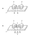
本実施形態の説明に先立ち、本実施形態の基礎となる予備的事項について説明する。
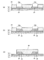
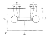
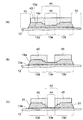
図3〜図7は、本実施形態に係る抵抗素子の製造途中の断面図である。
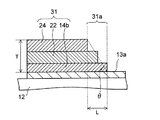
第1実施形態では、図7(b)に示したように、電極31の裾野部分31aを雛壇状にした。これに対し、本実施形態では、その裾野部分31aを以下のようにして傾斜させる。
本実施形態では、第1実施形態又は第2実施形態で形成した抵抗素子を備えた回路基板について説明する。
本実施形態では、第3実施形態と同様に、回路基板に第1実施形態や第2実施形態で作製した抵抗素子を適用する。

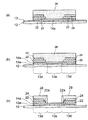
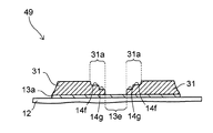
図23〜図26は、本実施形態に係る抵抗素子の製造途中の断面図である。なお、これらの図は第1実施形態の図3(b)の一部領域Aを拡大したものである。また、図23〜図26において、第1実施形態で説明したのと同じ要素には同じ符号を付し、以下ではその説明を省略する。
前記基材の上方に形成された抵抗素子とを有し、
前記抵抗素子が、電極部と延在部とを備えた抵抗パターンと、前記抵抗パターンの前記電極部上に形成され、前記延在部に向かって厚さが薄くなる裾野部分を備えた電極とを有することを特徴とする回路基板。
前記基材が、前記コア基板の上方に形成されたことを特徴とする付記1〜4のいずれかに記載の回路基板。
前記抵抗パターンの前記電極部上に形成され、前記延在部に向かって厚さが薄くなる裾野部分を備えた電極と、
を有することを特徴とする抵抗素子。
前記導体層の厚さを薄くする工程と、
前記導体層の上に、第1の電極パターンを選択的に形成する工程と、
前記導体層の厚さを薄くした後、前記導体層をパターニングすることにより導体パターンを形成する工程と、
前記導体パターンをマスクにして前記抵抗体層をエッチングすることにより、前記第1の電極パターンから前記基材の横方向に延在する延在部を備えた抵抗パターンを形成する工程と、
前記抵抗パターンを形成した後、前記導体パターンをパターニングすることにより、前記第1の電極パターンよりも前記延在部側に延びた第2の電極パターンを形成する工程と、
を有することを特徴とする回路基板の製造方法。
前記絶縁層の上に配線層を形成する工程と、
前記基材、前記絶縁層、及び前記配線層を加熱しながらプレスすることにより積層体を形成する工程とを更に有することを特徴とする付記9〜14のいずれかに記載の回路基板の製造方法。
Claims (10)
- 基材と、
前記基材の上方に形成された抵抗素子とを有し、
前記抵抗素子が、電極部と延在部とを備えた抵抗パターンと、前記抵抗パターンの前記
電極部上に形成され、前記延在部に向かって厚さが段階的に薄くなる裾野部分を備えた電極とを有することを特徴とする回路基板。 - 前記抵抗素子の上に、絶縁層と配線パターンとが交互に複数積層されたことを特徴とする請求項1に記載の回路基板。
- 前記電極が複数層から成ることを特徴とする請求項1又は請求項2に記載の回路基板。
- 絶縁層の上に形成され、電極部と延在部とを備えた抵抗パターンと、
前記抵抗パターンの前記電極部上に形成され、前記延在部に向かって段階的に厚さが段階的に薄くなる裾野部分を備えた電極と、
を有することを特徴とする抵抗素子。 - 前記電極は、前記抵抗パターンよりもシート抵抗の低い材料よりなることを特徴とする請求項4に記載の抵抗素子。
- 前記電極が複数層から成ることを特徴とする請求項4又は請求項5に記載の抵抗素子。
- 基材の上方に抵抗体層と導体層とを順に形成する工程と、
前記導体層の厚さを薄くする工程と、
前記導体層の上に、第1の電極パターンを選択的に形成する工程と、
前記導体層の厚さを薄くした後、前記導体層をパターニングすることにより導体パター
ンを形成する工程と、
前記導体パターンをマスクにして前記抵抗体層をエッチングすることにより、前記第1の電極パターンから前記基材の横方向に延在する延在部を備えた抵抗パターンを形成する工程と、
前記抵抗パターンを形成した後、前記導体パターンをパターニングすることにより、前記第1の電極パターンよりも前記延在部側に延びた第2の電極パターンを形成する工程と、
を有することを特徴とする回路基板の製造方法。 - 前記第2の電極パターンを形成する工程は、前記第1の電極パターンの側面のうち前記延在部寄りの側面と、前記第1の電極パターンの上面とを覆うレジストパターンを形成し、該レジストパターンをマスクにしながら前記導体パターンをウエットエッチングすることにより行われることを特徴とする請求項7に記載の回路基板の製造方法。
- 前記第2の電極パターンを形成する工程は、前記第1の電極パターンの側面のうち前記延在部寄りの側面から後退したレジストパターンを前記第1の電極パターンの上に形成し、該レジストパターンをマスクにしながら前記導体パターンをウエットエッチングすることにより行われることを特徴とする請求項7に記載の回路基板の製造方法。
- 前記導体パターンを形成する工程は、前記導体層の上にレジストパターンを形成し、該
レジストパターンをマスクにして前記導体層をウエットエッチングすることにより行われ
ることを特徴とする請求項7に記載の回路基板の製造方法。
Priority Applications (2)
| Application Number | Priority Date | Filing Date | Title |
|---|---|---|---|
| JP2009230606A JP5391981B2 (ja) | 2009-02-02 | 2009-10-02 | 回路基板とその製造方法、及び抵抗素子 |
| US12/689,353 US8642894B2 (en) | 2009-02-02 | 2010-01-19 | Circuit board, method of manufacturing the same, and resistance element |
Applications Claiming Priority (3)
| Application Number | Priority Date | Filing Date | Title |
|---|---|---|---|
| JP2009021913 | 2009-02-02 | ||
| JP2009021913 | 2009-02-02 | ||
| JP2009230606A JP5391981B2 (ja) | 2009-02-02 | 2009-10-02 | 回路基板とその製造方法、及び抵抗素子 |
Publications (2)
| Publication Number | Publication Date |
|---|---|
| JP2010199540A JP2010199540A (ja) | 2010-09-09 |
| JP5391981B2 true JP5391981B2 (ja) | 2014-01-15 |
Family
ID=42396763
Family Applications (1)
| Application Number | Title | Priority Date | Filing Date |
|---|---|---|---|
| JP2009230606A Expired - Fee Related JP5391981B2 (ja) | 2009-02-02 | 2009-10-02 | 回路基板とその製造方法、及び抵抗素子 |
Country Status (2)
| Country | Link |
|---|---|
| US (1) | US8642894B2 (ja) |
| JP (1) | JP5391981B2 (ja) |
Families Citing this family (8)
| Publication number | Priority date | Publication date | Assignee | Title |
|---|---|---|---|---|
| US9472425B2 (en) * | 2015-03-19 | 2016-10-18 | Qualcomm Incorporated | Power distribution improvement using pseudo-ESR control of an embedded passive capacitor |
| JP2016219452A (ja) * | 2015-05-14 | 2016-12-22 | 富士通株式会社 | 多層基板及び多層基板の製造方法 |
| US11239185B2 (en) * | 2017-11-03 | 2022-02-01 | Dialog Semiconductor (Uk) Limited | Embedded resistor-capacitor film for fan out wafer level packaging |
| CN112586092B (zh) * | 2018-08-28 | 2024-10-25 | 京瓷株式会社 | 布线基板以及电子装置 |
| CN109688716A (zh) * | 2018-12-20 | 2019-04-26 | 广州陶积电电子科技有限公司 | 一种带灯杯的线路板及其制作工艺 |
| JP6979486B1 (ja) * | 2020-06-25 | 2021-12-15 | 日東電工株式会社 | 配線回路基板集合体シートおよびその製造方法 |
| US12193166B2 (en) * | 2022-04-13 | 2025-01-07 | SanDisk Technologies, Inc. | Printed circuit board having a sacrificial pad to mitigate galvanic corrosion |
| DE102024113639A1 (de) | 2024-05-15 | 2025-11-20 | ILFA Industrieelektronik und Leiterplattenfertigung aller Art Gesellschaft mit beschränkter Haftung | Verfahren zur Herstellung einer Leiterplatte |
Family Cites Families (18)
| Publication number | Priority date | Publication date | Assignee | Title |
|---|---|---|---|---|
| JPS5378050A (en) * | 1976-12-21 | 1978-07-11 | Nitto Electric Ind Co | Multilayer resistance circuit board |
| JPS58116269U (ja) * | 1982-01-30 | 1983-08-08 | 日本メクトロン株式会社 | 可撓性回路基板 |
| JPS63128787A (ja) * | 1986-11-19 | 1988-06-01 | 富士通株式会社 | 混成集積回路の製造方法 |
| US5243320A (en) * | 1988-02-26 | 1993-09-07 | Gould Inc. | Resistive metal layers and method for making same |
| JPH04307701A (ja) * | 1991-04-04 | 1992-10-29 | Toppan Printing Co Ltd | プリント配線板とその中間体及びその製造方法 |
| JP3227800B2 (ja) | 1992-06-30 | 2001-11-12 | 富士ゼロックス株式会社 | 脆性板切断方法およびその装置 |
| JP3199563B2 (ja) * | 1994-04-27 | 2001-08-20 | 京セラ株式会社 | 配線基板 |
| JPH09246723A (ja) * | 1996-03-11 | 1997-09-19 | Sumitomo Kinzoku Electro Device:Kk | 低温焼成セラミック回路基板 |
| JP4334659B2 (ja) * | 1999-03-31 | 2009-09-30 | 京セラ株式会社 | セラミック配線基板とその製造方法 |
| JP4385434B2 (ja) * | 1999-04-13 | 2009-12-16 | 株式会社デンソー | 厚膜回路基板及びその製造方法 |
| JP4307701B2 (ja) | 1999-12-10 | 2009-08-05 | 富士フイルム株式会社 | 光電変換素子および光電池 |
| EP1191551B1 (en) * | 2000-09-22 | 2005-11-23 | Nikko Materials USA, Inc. | Resistor component with multiple layers of resistive material |
| WO2004055836A1 (ja) * | 2002-12-16 | 2004-07-01 | Koa Kabushiki Kaisha | 抵抗材料、抵抗体、抵抗器、および抵抗器の製造方法 |
| WO2004086493A1 (ja) | 2003-03-25 | 2004-10-07 | Fujitsu Limited | 電子部品搭載基板の製造方法 |
| JP4396426B2 (ja) * | 2004-07-08 | 2010-01-13 | 凸版印刷株式会社 | 抵抗素子及びその抵抗素子を内蔵した多層プリント配線板 |
| JP2007067035A (ja) * | 2005-08-30 | 2007-03-15 | Toppan Printing Co Ltd | 抵抗素子および抵抗素子の製造方法 |
| JP4855753B2 (ja) * | 2005-10-03 | 2012-01-18 | 富士通株式会社 | 多層配線基板及びその製造方法 |
| JP5205904B2 (ja) | 2006-09-29 | 2013-06-05 | 大日本印刷株式会社 | 金属酸化物膜の製造方法、および積層体 |
-
2009
- 2009-10-02 JP JP2009230606A patent/JP5391981B2/ja not_active Expired - Fee Related
-
2010
- 2010-01-19 US US12/689,353 patent/US8642894B2/en not_active Expired - Fee Related
Also Published As
| Publication number | Publication date |
|---|---|
| US20100193225A1 (en) | 2010-08-05 |
| US8642894B2 (en) | 2014-02-04 |
| JP2010199540A (ja) | 2010-09-09 |
Similar Documents
| Publication | Publication Date | Title |
|---|---|---|
| JP2010199540A (ja) | 回路基板とその製造方法、及び抵抗素子 | |
| TWI222201B (en) | Method of producing multilayered circuit board for semiconductor device | |
| CN101518163B (zh) | 刚挠性印刷电路板及该刚挠性印刷电路板的制造方法 | |
| US9773747B2 (en) | Wiring substrate and method for manufacturing wiring subtrate | |
| JP6460220B1 (ja) | コイル部品及びその製造方法 | |
| US10847300B2 (en) | Inductor and method of manufacturing the same | |
| US11266016B2 (en) | Resin multilayer substrate and electronic apparatus | |
| JP6625872B2 (ja) | 配線基板及び配線基板の製造方法 | |
| US20180218830A1 (en) | Inductor device | |
| US9392684B2 (en) | Wiring substrate and method for manufacturing wiring substrate | |
| US20140318834A1 (en) | Wiring board and method for manufacturing the same | |
| CN110073729A (zh) | 配线基板、多层配线基板以及配线基板的制造方法 | |
| JP5191889B2 (ja) | 部品内蔵配線板の製造方法 | |
| US9420696B2 (en) | Method of manufacturing wiring substrate | |
| US20180061555A1 (en) | Inductor and method of manufacturing the same | |
| CN104780723A (zh) | 布线基板的制造方法 | |
| JP2019021863A (ja) | 多層基板 | |
| KR20120130515A (ko) | 회로 기판 및 그의 제조 방법 | |
| CN115413112A (zh) | 布线电路基板和其制造方法 | |
| US20220369469A1 (en) | Method of manufacturing printed wiring board | |
| JP2013080823A (ja) | プリント配線板及びその製造方法 | |
| TW200906258A (en) | Method for fabricating a circuit board | |
| JP2007013208A (ja) | プリント配線基板の製造方法 | |
| JP5223893B2 (ja) | 部品内蔵配線板、部品内蔵配線板の製造方法 | |
| JP4687072B2 (ja) | 配線基板の製造方法及び配線基板 |
Legal Events
| Date | Code | Title | Description |
|---|---|---|---|
| A621 | Written request for application examination |
Free format text: JAPANESE INTERMEDIATE CODE: A621 Effective date: 20120605 |
|
| A977 | Report on retrieval |
Free format text: JAPANESE INTERMEDIATE CODE: A971007 Effective date: 20130410 |
|
| A131 | Notification of reasons for refusal |
Free format text: JAPANESE INTERMEDIATE CODE: A131 Effective date: 20130514 |
|
| A521 | Written amendment |
Free format text: JAPANESE INTERMEDIATE CODE: A523 Effective date: 20130625 |
|
| TRDD | Decision of grant or rejection written | ||
| A01 | Written decision to grant a patent or to grant a registration (utility model) |
Free format text: JAPANESE INTERMEDIATE CODE: A01 Effective date: 20130917 |
|
| A61 | First payment of annual fees (during grant procedure) |
Free format text: JAPANESE INTERMEDIATE CODE: A61 Effective date: 20130930 |
|
| R150 | Certificate of patent or registration of utility model |
Ref document number: 5391981 Country of ref document: JP Free format text: JAPANESE INTERMEDIATE CODE: R150 Free format text: JAPANESE INTERMEDIATE CODE: R150 |
|
| LAPS | Cancellation because of no payment of annual fees |