JP5399245B2 - 処理システムでワークピースを扱うための装置及び方法 - Google Patents
処理システムでワークピースを扱うための装置及び方法 Download PDFInfo
- Publication number
- JP5399245B2 JP5399245B2 JP2009525702A JP2009525702A JP5399245B2 JP 5399245 B2 JP5399245 B2 JP 5399245B2 JP 2009525702 A JP2009525702 A JP 2009525702A JP 2009525702 A JP2009525702 A JP 2009525702A JP 5399245 B2 JP5399245 B2 JP 5399245B2
- Authority
- JP
- Japan
- Prior art keywords
- workpiece
- plate member
- lower electrode
- base portion
- upper electrode
- Prior art date
- Legal status (The legal status is an assumption and is not a legal conclusion. Google has not performed a legal analysis and makes no representation as to the accuracy of the status listed.)
- Expired - Fee Related
Links
Images


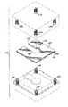


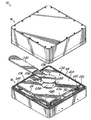


Classifications
-
- H—ELECTRICITY
- H10—SEMICONDUCTOR DEVICES; ELECTRIC SOLID-STATE DEVICES NOT OTHERWISE PROVIDED FOR
- H10P—GENERIC PROCESSES OR APPARATUS FOR THE MANUFACTURE OR TREATMENT OF DEVICES COVERED BY CLASS H10
- H10P72/00—Handling or holding of wafers, substrates or devices during manufacture or treatment thereof
- H10P72/30—Handling or holding of wafers, substrates or devices during manufacture or treatment thereof for conveying, e.g. between different workstations
- H10P72/33—Handling or holding of wafers, substrates or devices during manufacture or treatment thereof for conveying, e.g. between different workstations into and out of processing chamber
- H10P72/3306—Horizontal transfer of a single workpiece
-
- H—ELECTRICITY
- H10—SEMICONDUCTOR DEVICES; ELECTRIC SOLID-STATE DEVICES NOT OTHERWISE PROVIDED FOR
- H10P—GENERIC PROCESSES OR APPARATUS FOR THE MANUFACTURE OR TREATMENT OF DEVICES COVERED BY CLASS H10
- H10P72/00—Handling or holding of wafers, substrates or devices during manufacture or treatment thereof
- H10P72/04—Apparatus for manufacture or treatment
- H10P72/0451—Apparatus for manufacturing or treating in a plurality of work-stations
- H10P72/0462—Apparatus for manufacturing or treating in a plurality of work-stations characterised by the construction of the processing chambers, e.g. modular processing chambers
-
- H—ELECTRICITY
- H10—SEMICONDUCTOR DEVICES; ELECTRIC SOLID-STATE DEVICES NOT OTHERWISE PROVIDED FOR
- H10P—GENERIC PROCESSES OR APPARATUS FOR THE MANUFACTURE OR TREATMENT OF DEVICES COVERED BY CLASS H10
- H10P72/00—Handling or holding of wafers, substrates or devices during manufacture or treatment thereof
- H10P72/70—Handling or holding of wafers, substrates or devices during manufacture or treatment thereof for supporting or gripping
- H10P72/76—Handling or holding of wafers, substrates or devices during manufacture or treatment thereof for supporting or gripping using mechanical means, e.g. clamps or pinches
- H10P72/7604—Handling or holding of wafers, substrates or devices during manufacture or treatment thereof for supporting or gripping using mechanical means, e.g. clamps or pinches the wafers being placed on a susceptor, stage or support
-
- H—ELECTRICITY
- H10—SEMICONDUCTOR DEVICES; ELECTRIC SOLID-STATE DEVICES NOT OTHERWISE PROVIDED FOR
- H10P—GENERIC PROCESSES OR APPARATUS FOR THE MANUFACTURE OR TREATMENT OF DEVICES COVERED BY CLASS H10
- H10P72/00—Handling or holding of wafers, substrates or devices during manufacture or treatment thereof
- H10P72/70—Handling or holding of wafers, substrates or devices during manufacture or treatment thereof for supporting or gripping
- H10P72/76—Handling or holding of wafers, substrates or devices during manufacture or treatment thereof for supporting or gripping using mechanical means, e.g. clamps or pinches
- H10P72/7604—Handling or holding of wafers, substrates or devices during manufacture or treatment thereof for supporting or gripping using mechanical means, e.g. clamps or pinches the wafers being placed on a susceptor, stage or support
- H10P72/7612—Handling or holding of wafers, substrates or devices during manufacture or treatment thereof for supporting or gripping using mechanical means, e.g. clamps or pinches the wafers being placed on a susceptor, stage or support characterised by lifting arrangements, e.g. lift pins
-
- H—ELECTRICITY
- H10—SEMICONDUCTOR DEVICES; ELECTRIC SOLID-STATE DEVICES NOT OTHERWISE PROVIDED FOR
- H10P—GENERIC PROCESSES OR APPARATUS FOR THE MANUFACTURE OR TREATMENT OF DEVICES COVERED BY CLASS H10
- H10P72/00—Handling or holding of wafers, substrates or devices during manufacture or treatment thereof
- H10P72/70—Handling or holding of wafers, substrates or devices during manufacture or treatment thereof for supporting or gripping
- H10P72/78—Handling or holding of wafers, substrates or devices during manufacture or treatment thereof for supporting or gripping using vacuum or suction, e.g. Bernoulli chucks
Landscapes
- Drying Of Semiconductors (AREA)
- Plasma Technology (AREA)
- Electrical Discharge Machining, Electrochemical Machining, And Combined Machining (AREA)
- Specific Conveyance Elements (AREA)
Applications Claiming Priority (3)
| Application Number | Priority Date | Filing Date | Title |
|---|---|---|---|
| US82317506P | 2006-08-22 | 2006-08-22 | |
| US60/823,175 | 2006-08-22 | ||
| PCT/US2007/076205 WO2008024681A2 (fr) | 2006-08-22 | 2007-08-17 | Appareil et procédés permettant de manipuler des pieces à travailler dans un système de traitement |
Publications (2)
| Publication Number | Publication Date |
|---|---|
| JP2010502016A JP2010502016A (ja) | 2010-01-21 |
| JP5399245B2 true JP5399245B2 (ja) | 2014-01-29 |
Family
ID=39107548
Family Applications (1)
| Application Number | Title | Priority Date | Filing Date |
|---|---|---|---|
| JP2009525702A Expired - Fee Related JP5399245B2 (ja) | 2006-08-22 | 2007-08-17 | 処理システムでワークピースを扱うための装置及び方法 |
Country Status (6)
| Country | Link |
|---|---|
| US (2) | US8245663B2 (fr) |
| JP (1) | JP5399245B2 (fr) |
| KR (1) | KR101410706B1 (fr) |
| CN (1) | CN101506066B (fr) |
| SG (1) | SG174093A1 (fr) |
| WO (1) | WO2008024681A2 (fr) |
Families Citing this family (11)
| Publication number | Priority date | Publication date | Assignee | Title |
|---|---|---|---|---|
| WO2008024681A2 (fr) * | 2006-08-22 | 2008-02-28 | Nordson Corporation | Appareil et procédés permettant de manipuler des pieces à travailler dans un système de traitement |
| US20080296261A1 (en) * | 2007-06-01 | 2008-12-04 | Nordson Corporation | Apparatus and methods for improving treatment uniformity in a plasma process |
| US9385017B2 (en) * | 2012-08-06 | 2016-07-05 | Nordson Corporation | Apparatus and methods for handling workpieces of different sizes |
| US9355882B2 (en) * | 2013-12-04 | 2016-05-31 | Taiwan Semiconductor Manufacturing Co., Ltd. | Transfer module for bowed wafers |
| US9881826B2 (en) * | 2014-10-24 | 2018-01-30 | Lam Research Corporation | Buffer station with single exit-flow direction |
| JP6473974B2 (ja) | 2016-09-30 | 2019-02-27 | パナソニックIpマネジメント株式会社 | プラズマ処理装置およびプラズマ処理方法 |
| JP6524536B2 (ja) | 2016-11-09 | 2019-06-05 | パナソニックIpマネジメント株式会社 | プラズマ処理装置およびプラズマ処理方法 |
| US10453727B2 (en) * | 2016-11-10 | 2019-10-22 | Applied Materials, Inc. | Electronic device manufacturing load port apparatus, systems, and methods |
| JP7451490B2 (ja) * | 2018-07-30 | 2024-03-18 | ノードソン コーポレーション | プラズマを用いたワーク処理用のシステム |
| CN113136564B (zh) * | 2020-12-31 | 2023-02-24 | 拓荆科技股份有限公司 | 单腔镀膜系统 |
| JP7846969B2 (ja) * | 2021-06-30 | 2026-04-16 | 東京エレクトロン株式会社 | プラズマ処理チャンバ、プラズマ処理装置及び締結部材 |
Family Cites Families (21)
| Publication number | Priority date | Publication date | Assignee | Title |
|---|---|---|---|---|
| JPH0733973A (ja) | 1993-07-16 | 1995-02-03 | Mitsubishi Chem Corp | 熱可塑性樹脂組成物 |
| JP2601180Y2 (ja) * | 1993-12-06 | 1999-11-08 | 日新電機株式会社 | 基板保持装置 |
| TW254030B (en) * | 1994-03-18 | 1995-08-11 | Anelva Corp | Mechanic escape mechanism for substrate |
| JP3608121B2 (ja) * | 1994-03-18 | 2005-01-05 | アネルバ株式会社 | 基板の機械的脱離機構およびその機構を用いた脱離方法 |
| JPH08148471A (ja) * | 1994-11-25 | 1996-06-07 | Sumitomo Metal Ind Ltd | プラズマエッチング装置 |
| US5823416A (en) | 1995-07-28 | 1998-10-20 | Matsushita Electric Industrial Co., Ltd. | Apparatus and method for surface treatment, and apparatus and method for wire bonding using the surface treatment apparatus |
| US6203582B1 (en) | 1996-07-15 | 2001-03-20 | Semitool, Inc. | Modular semiconductor workpiece processing tool |
| JP3201302B2 (ja) | 1997-02-10 | 2001-08-20 | 松下電器産業株式会社 | 基板のプラズマクリーニング装置 |
| TW464919B (en) * | 1999-03-30 | 2001-11-21 | Tokyo Electron Ltd | Plasma processing apparatus, maintenance method thereof and setting method thereof |
| JP2002009133A (ja) | 2000-06-26 | 2002-01-11 | Canon Inc | 基板搬送装置 |
| AU2001282879A1 (en) | 2000-07-08 | 2002-01-21 | Semitool, Inc. | Methods and apparatus for processing microelectronic workpieces using metrology |
| JP3587788B2 (ja) * | 2001-02-27 | 2004-11-10 | 住友精密工業株式会社 | 昇降式基板処理装置及びこれを備えた基板処理システム |
| JP4850372B2 (ja) * | 2001-09-28 | 2012-01-11 | キヤノンアネルバ株式会社 | 基板処理装置 |
| JP4244555B2 (ja) * | 2002-02-25 | 2009-03-25 | 東京エレクトロン株式会社 | 被処理体の支持機構 |
| JP3948325B2 (ja) * | 2002-04-02 | 2007-07-25 | 松下電器産業株式会社 | フィルム基板処理方法 |
| US7013834B2 (en) * | 2002-04-19 | 2006-03-21 | Nordson Corporation | Plasma treatment system |
| US6846380B2 (en) | 2002-06-13 | 2005-01-25 | The Boc Group, Inc. | Substrate processing apparatus and related systems and methods |
| US7845309B2 (en) | 2004-07-13 | 2010-12-07 | Nordson Corporation | Ultra high speed uniform plasma processing system |
| US20060090703A1 (en) | 2004-11-01 | 2006-05-04 | Tokyo Electron Limited | Substrate processing method, system and program |
| WO2008024681A2 (fr) * | 2006-08-22 | 2008-02-28 | Nordson Corporation | Appareil et procédés permettant de manipuler des pieces à travailler dans un système de traitement |
| US20080296261A1 (en) | 2007-06-01 | 2008-12-04 | Nordson Corporation | Apparatus and methods for improving treatment uniformity in a plasma process |
-
2007
- 2007-08-17 WO PCT/US2007/076205 patent/WO2008024681A2/fr not_active Ceased
- 2007-08-17 CN CN200780031329.2A patent/CN101506066B/zh active Active
- 2007-08-17 KR KR1020097003480A patent/KR101410706B1/ko not_active Expired - Fee Related
- 2007-08-17 SG SG2011060548A patent/SG174093A1/en unknown
- 2007-08-17 JP JP2009525702A patent/JP5399245B2/ja not_active Expired - Fee Related
- 2007-08-17 US US12/376,175 patent/US8245663B2/en active Active
-
2012
- 2012-07-17 US US13/551,308 patent/US8986564B2/en not_active Expired - Fee Related
Also Published As
| Publication number | Publication date |
|---|---|
| SG174093A1 (en) | 2011-09-29 |
| WO2008024681A2 (fr) | 2008-02-28 |
| US8245663B2 (en) | 2012-08-21 |
| KR101410706B1 (ko) | 2014-06-25 |
| KR20090071544A (ko) | 2009-07-01 |
| CN101506066A (zh) | 2009-08-12 |
| US8986564B2 (en) | 2015-03-24 |
| US20120279946A1 (en) | 2012-11-08 |
| WO2008024681A3 (fr) | 2008-04-24 |
| JP2010502016A (ja) | 2010-01-21 |
| CN101506066B (zh) | 2012-11-28 |
| US20090311088A1 (en) | 2009-12-17 |
Similar Documents
| Publication | Publication Date | Title |
|---|---|---|
| JP5399245B2 (ja) | 処理システムでワークピースを扱うための装置及び方法 | |
| CN101681785B (zh) | 用于提高等离子体工艺中的处理均匀性的设备和方法 | |
| JP5188385B2 (ja) | プラズマ処理装置及びプラズマ処理装置の運転方法 | |
| KR102168255B1 (ko) | 다른 크기의 워크피스를 취급하기 위한 장치 및 방법 | |
| KR101791991B1 (ko) | 플라즈마 처리 장치 | |
| CN1327493C (zh) | 处理装置部件的装配机构及其装配方法 | |
| KR20190029365A (ko) | 리프트 핀 조립체, 이를 갖는 기판 지지 유닛 및 기판 처리 장치 | |
| KR101672856B1 (ko) | 플라즈마 처리 장치 | |
| KR100682216B1 (ko) | 진공 처리 장치 | |
| KR20190000798A (ko) | 플라즈마 처리 장치 | |
| US20210118648A1 (en) | Substrate processing system and method for replacing edge ring | |
| CN115483130A (zh) | 基板处理设备和基板处理系统 | |
| US20050066902A1 (en) | Method and apparatus for plasma processing | |
| JP2018078197A (ja) | プラズマ処理装置およびプラズマ処理方法 | |
| JP2006253365A (ja) | プラズマ処理装置 | |
| JP2019160468A (ja) | プラズマ処理装置 |
Legal Events
| Date | Code | Title | Description |
|---|---|---|---|
| A621 | Written request for application examination |
Free format text: JAPANESE INTERMEDIATE CODE: A621 Effective date: 20100811 |
|
| A977 | Report on retrieval |
Free format text: JAPANESE INTERMEDIATE CODE: A971007 Effective date: 20120116 |
|
| A131 | Notification of reasons for refusal |
Free format text: JAPANESE INTERMEDIATE CODE: A131 Effective date: 20120123 |
|
| A601 | Written request for extension of time |
Free format text: JAPANESE INTERMEDIATE CODE: A601 Effective date: 20120423 |
|
| A602 | Written permission of extension of time |
Free format text: JAPANESE INTERMEDIATE CODE: A602 Effective date: 20120501 |
|
| A521 | Request for written amendment filed |
Free format text: JAPANESE INTERMEDIATE CODE: A523 Effective date: 20120723 |
|
| A131 | Notification of reasons for refusal |
Free format text: JAPANESE INTERMEDIATE CODE: A131 Effective date: 20130328 |
|
| A521 | Request for written amendment filed |
Free format text: JAPANESE INTERMEDIATE CODE: A523 Effective date: 20130628 |
|
| A131 | Notification of reasons for refusal |
Free format text: JAPANESE INTERMEDIATE CODE: A131 Effective date: 20130827 |
|
| A521 | Request for written amendment filed |
Free format text: JAPANESE INTERMEDIATE CODE: A523 Effective date: 20130829 |
|
| TRDD | Decision of grant or rejection written | ||
| A01 | Written decision to grant a patent or to grant a registration (utility model) |
Free format text: JAPANESE INTERMEDIATE CODE: A01 Effective date: 20130924 |
|
| A61 | First payment of annual fees (during grant procedure) |
Free format text: JAPANESE INTERMEDIATE CODE: A61 Effective date: 20131023 |
|
| R150 | Certificate of patent or registration of utility model |
Ref document number: 5399245 Country of ref document: JP Free format text: JAPANESE INTERMEDIATE CODE: R150 Free format text: JAPANESE INTERMEDIATE CODE: R150 |
|
| R250 | Receipt of annual fees |
Free format text: JAPANESE INTERMEDIATE CODE: R250 |
|
| R250 | Receipt of annual fees |
Free format text: JAPANESE INTERMEDIATE CODE: R250 |
|
| R250 | Receipt of annual fees |
Free format text: JAPANESE INTERMEDIATE CODE: R250 |
|
| R250 | Receipt of annual fees |
Free format text: JAPANESE INTERMEDIATE CODE: R250 |
|
| R250 | Receipt of annual fees |
Free format text: JAPANESE INTERMEDIATE CODE: R250 |
|
| LAPS | Cancellation because of no payment of annual fees |