JP5408954B2 - 撮像装置、及び撮像システム - Google Patents
撮像装置、及び撮像システム Download PDFInfo
- Publication number
- JP5408954B2 JP5408954B2 JP2008269183A JP2008269183A JP5408954B2 JP 5408954 B2 JP5408954 B2 JP 5408954B2 JP 2008269183 A JP2008269183 A JP 2008269183A JP 2008269183 A JP2008269183 A JP 2008269183A JP 5408954 B2 JP5408954 B2 JP 5408954B2
- Authority
- JP
- Japan
- Prior art keywords
- pixel
- unit
- vertical
- photoelectric conversion
- wiring layer
- Prior art date
- Legal status (The legal status is an assumption and is not a legal conclusion. Google has not performed a legal analysis and makes no representation as to the accuracy of the status listed.)
- Expired - Fee Related
Links
Images






Classifications
-
- H—ELECTRICITY
- H04—ELECTRIC COMMUNICATION TECHNIQUE
- H04N—PICTORIAL COMMUNICATION, e.g. TELEVISION
- H04N25/00—Circuitry of solid-state image sensors [SSIS]; Control thereof
- H04N25/70—SSIS architectures; Circuits associated therewith
- H04N25/76—Addressed sensors, e.g. MOS or CMOS sensors
- H04N25/77—Pixel circuitry, e.g. memories, A/D converters, pixel amplifiers, shared circuits or shared components
- H04N25/778—Pixel circuitry, e.g. memories, A/D converters, pixel amplifiers, shared circuits or shared components comprising amplifiers shared between a plurality of pixels, i.e. at least one part of the amplifier must be on the sensor array itself
-
- H—ELECTRICITY
- H04—ELECTRIC COMMUNICATION TECHNIQUE
- H04N—PICTORIAL COMMUNICATION, e.g. TELEVISION
- H04N25/00—Circuitry of solid-state image sensors [SSIS]; Control thereof
- H04N25/10—Circuitry of solid-state image sensors [SSIS]; Control thereof for transforming different wavelengths into image signals
- H04N25/11—Arrangement of colour filter arrays [CFA]; Filter mosaics
- H04N25/13—Arrangement of colour filter arrays [CFA]; Filter mosaics characterised by the spectral characteristics of the filter elements
- H04N25/134—Arrangement of colour filter arrays [CFA]; Filter mosaics characterised by the spectral characteristics of the filter elements based on three different wavelength filter elements
-
- H—ELECTRICITY
- H10—SEMICONDUCTOR DEVICES; ELECTRIC SOLID-STATE DEVICES NOT OTHERWISE PROVIDED FOR
- H10F—INORGANIC SEMICONDUCTOR DEVICES SENSITIVE TO INFRARED RADIATION, LIGHT, ELECTROMAGNETIC RADIATION OF SHORTER WAVELENGTH OR CORPUSCULAR RADIATION
- H10F39/00—Integrated devices, or assemblies of multiple devices, comprising at least one element covered by group H10F30/00, e.g. radiation detectors comprising photodiode arrays
- H10F39/80—Constructional details of image sensors
- H10F39/802—Geometry or disposition of elements in pixels, e.g. address-lines or gate electrodes
-
- H—ELECTRICITY
- H10—SEMICONDUCTOR DEVICES; ELECTRIC SOLID-STATE DEVICES NOT OTHERWISE PROVIDED FOR
- H10F—INORGANIC SEMICONDUCTOR DEVICES SENSITIVE TO INFRARED RADIATION, LIGHT, ELECTROMAGNETIC RADIATION OF SHORTER WAVELENGTH OR CORPUSCULAR RADIATION
- H10F39/00—Integrated devices, or assemblies of multiple devices, comprising at least one element covered by group H10F30/00, e.g. radiation detectors comprising photodiode arrays
- H10F39/80—Constructional details of image sensors
- H10F39/803—Pixels having integrated switching, control, storage or amplification elements
- H10F39/8037—Pixels having integrated switching, control, storage or amplification elements the integrated elements comprising a transistor
-
- H—ELECTRICITY
- H10—SEMICONDUCTOR DEVICES; ELECTRIC SOLID-STATE DEVICES NOT OTHERWISE PROVIDED FOR
- H10F—INORGANIC SEMICONDUCTOR DEVICES SENSITIVE TO INFRARED RADIATION, LIGHT, ELECTROMAGNETIC RADIATION OF SHORTER WAVELENGTH OR CORPUSCULAR RADIATION
- H10F39/00—Integrated devices, or assemblies of multiple devices, comprising at least one element covered by group H10F30/00, e.g. radiation detectors comprising photodiode arrays
- H10F39/80—Constructional details of image sensors
- H10F39/806—Optical elements or arrangements associated with the image sensors
- H10F39/8063—Microlenses
-
- H—ELECTRICITY
- H10—SEMICONDUCTOR DEVICES; ELECTRIC SOLID-STATE DEVICES NOT OTHERWISE PROVIDED FOR
- H10F—INORGANIC SEMICONDUCTOR DEVICES SENSITIVE TO INFRARED RADIATION, LIGHT, ELECTROMAGNETIC RADIATION OF SHORTER WAVELENGTH OR CORPUSCULAR RADIATION
- H10F39/00—Integrated devices, or assemblies of multiple devices, comprising at least one element covered by group H10F30/00, e.g. radiation detectors comprising photodiode arrays
- H10F39/80—Constructional details of image sensors
- H10F39/813—Electronic components shared by multiple pixels, e.g. one amplifier shared by two pixels
-
- H—ELECTRICITY
- H10—SEMICONDUCTOR DEVICES; ELECTRIC SOLID-STATE DEVICES NOT OTHERWISE PROVIDED FOR
- H10D—INORGANIC ELECTRIC SEMICONDUCTOR DEVICES
- H10D89/00—Aspects of integrated devices not covered by groups H10D84/00 - H10D88/00
- H10D89/10—Integrated device layouts
-
- H—ELECTRICITY
- H10—SEMICONDUCTOR DEVICES; ELECTRIC SOLID-STATE DEVICES NOT OTHERWISE PROVIDED FOR
- H10F—INORGANIC SEMICONDUCTOR DEVICES SENSITIVE TO INFRARED RADIATION, LIGHT, ELECTROMAGNETIC RADIATION OF SHORTER WAVELENGTH OR CORPUSCULAR RADIATION
- H10F39/00—Integrated devices, or assemblies of multiple devices, comprising at least one element covered by group H10F30/00, e.g. radiation detectors comprising photodiode arrays
- H10F39/10—Integrated devices
- H10F39/12—Image sensors
- H10F39/18—Complementary metal-oxide-semiconductor [CMOS] image sensors; Photodiode array image sensors
-
- H—ELECTRICITY
- H10—SEMICONDUCTOR DEVICES; ELECTRIC SOLID-STATE DEVICES NOT OTHERWISE PROVIDED FOR
- H10F—INORGANIC SEMICONDUCTOR DEVICES SENSITIVE TO INFRARED RADIATION, LIGHT, ELECTROMAGNETIC RADIATION OF SHORTER WAVELENGTH OR CORPUSCULAR RADIATION
- H10F39/00—Integrated devices, or assemblies of multiple devices, comprising at least one element covered by group H10F30/00, e.g. radiation detectors comprising photodiode arrays
- H10F39/80—Constructional details of image sensors
- H10F39/811—Interconnections
Landscapes
- Engineering & Computer Science (AREA)
- Multimedia (AREA)
- Signal Processing (AREA)
- Physics & Mathematics (AREA)
- Spectroscopy & Molecular Physics (AREA)
- Solid State Image Pick-Up Elements (AREA)
- Transforming Light Signals Into Electric Signals (AREA)
Description
Claims (10)
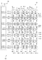
- 少なくとも、水平方向に隣接する2つの光電変換部と垂直方向に隣接する2つの光電変換部とを含む複数の光電変換部と、電荷を電圧に変換する電荷電圧変換部と、前記複数の光電変換部で発生した電荷を前記電荷電圧変換部へ転送する複数の転送トランジスタと、前記電荷電圧変換部の電圧に応じた信号を出力する増幅トランジスタと、前記電荷電圧変換部をリセットするリセットトランジスタとをそれぞれ含む複数の画素ユニットが水平方向及び垂直方向に配列された画素ユニット配列を含む撮像領域を有する半導体基板と、
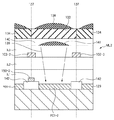
前記複数の画素ユニットのそれぞれにおける前記複数の光電変換部のそれぞれに対する開口領域を規定する多層配線構造と、
を備え、
前記多層配線構造は、
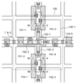
前記複数の光電変換部のそれぞれに対する開口領域の水平方向の輪郭辺を規定するように、前記半導体基板の上方に配された第1の配線層と、
前記複数の光電変換部のそれぞれに対する開口領域の垂直方向の輪郭辺を規定するように、前記第1の配線層の上方に配された第2の配線層と、を含み、
前記第2の配線層は、
前記増幅トランジスタから出力された信号を伝達するように垂直方向に延びた複数の垂直信号線と、
前記増幅トランジスタ又は前記リセットトランジスタへ電源電圧を供給するように垂直方向に延びた複数の垂直電源線と、を含み、
前記垂直信号線は、前記画素ユニットにおいて水平方向に隣接する前記光電変換部の間の領域の上方を垂直方向に延び、前記垂直電源線は、水平方向に隣接する前記画素ユニットの間の領域の上方を垂直方向に延びていて、
前記垂直電源線は、前記垂直電源線に対して水平方向の第1の側に隣接する前記画素ユニットにおける前記リセットトランジスタへ電源電圧を供給するとともに、前記垂直電源線に対して水平方向の第2の側に隣接する前記画素ユニットにおける前記増幅トランジスタへ電源電圧を供給する
ことを特徴とする撮像装置。 - 前記第2の配線層は、前記撮像領域における最上の配線層である
ことを特徴とする請求項1に記載の撮像装置。 - 前記半導体基板は、
前記撮像領域の周辺に位置し、前記画素ユニット配列から信号を読み出す読み出し部が配される周辺領域をさらに有し、
前記読み出し部は、
前記リセットトランジスタにより前記電荷電圧変換部がリセットされた状態で前記増幅トランジスタにより出力され前記垂直信号線を介して伝達されたノイズレベルをそれぞれ保持する2つのノイズレベル保持容量と、
前記光電変換部で発生した電荷が前記転送トランジスタにより前記電荷電圧変換部へ転送された状態で前記増幅トランジスタにより出力され前記垂直信号線を介して伝達された輝度レベルをそれぞれ保持する2つの輝度レベル保持容量と、を含む
ことを特徴とする請求項1又は2に記載の撮像装置。 - 前記複数の画素ユニットのそれぞれは、前記画素ユニットを選択状態又は非選択状態にする選択トランジスタをさらに含み、
前記増幅トランジスタと前記リセットトランジスタと前記選択トランジスタとのチャンネル長の方向は、水平方向に沿っている
ことを特徴とする請求項1から3のいずれか1項に記載の撮像装置。 - 前記第1の配線層は、
前記転送トランジスタのゲートへ制御信号を供給するように、水平方向に延びた転送制御線を含み、
前記転送制御線は、水平方向に隣接する2つ以上の前記画素ユニットに対して共通に設けられている
ことを特徴とする請求項1から4のいずれか1項に記載の撮像装置。 - 前記複数の画素ユニットのそれぞれは、前記複数の光電変換部に対応した複数のカラーフィルタをさらに含み、
前記複数のカラーフィルタの配列は、ベイヤー配列を形成している
ことを特徴とする請求項1から5のいずれか1項に記載の撮像装置。 - 前記垂直電源線の水平方向における一方の側面が、隣接する前記画素ユニットの一方における前記光電変換部に対する前記開口領域の前記輪郭辺を規定し、前記垂直電源線の水平方向における他方の側面が、当該隣接する前記画素ユニットの他方における前記光電変換部に対する前記開口領域の前記輪郭辺を規定するように、前記垂直電源線が配置されている、
ことを特徴とする請求項1から6のいずれか1項に記載の撮像装置。 - 前記垂直信号線の水平方向における一方の側面が、隣接する前記光電変換部の一方に対する前記開口領域の前記輪郭辺を規定し、前記垂直信号線の水平方向における他方の側面が、当該隣接する前記光電変換部の他方に対する前記開口領域の前記輪郭辺を規定するように、前記垂直信号線が配置されている、
ことを特徴とする請求項1から7のいずれか1項に記載の撮像装置。 - 前記増幅トランジスタおよび前記リセットトランジスタは、水平方向に沿って並ぶように配置されている、
ことを特徴とする請求項1から7のいずれか1項に記載の撮像装置。 - 請求項1から9のいずれか1項に記載の撮像装置と、
前記撮像装置の撮像面へ像を形成する光学系と、
前記撮像装置から出力された信号を処理して画像データを生成する信号処理部と、
を備えたことを特徴とする撮像システム。
Priority Applications (2)
| Application Number | Priority Date | Filing Date | Title |
|---|---|---|---|
| JP2008269183A JP5408954B2 (ja) | 2008-10-17 | 2008-10-17 | 撮像装置、及び撮像システム |
| US12/574,258 US8111311B2 (en) | 2008-10-17 | 2009-10-06 | Image sensing device and image sensing system |
Applications Claiming Priority (1)
| Application Number | Priority Date | Filing Date | Title |
|---|---|---|---|
| JP2008269183A JP5408954B2 (ja) | 2008-10-17 | 2008-10-17 | 撮像装置、及び撮像システム |
Publications (3)
| Publication Number | Publication Date |
|---|---|
| JP2010098193A JP2010098193A (ja) | 2010-04-30 |
| JP2010098193A5 JP2010098193A5 (ja) | 2011-11-04 |
| JP5408954B2 true JP5408954B2 (ja) | 2014-02-05 |
Family
ID=42108345
Family Applications (1)
| Application Number | Title | Priority Date | Filing Date |
|---|---|---|---|
| JP2008269183A Expired - Fee Related JP5408954B2 (ja) | 2008-10-17 | 2008-10-17 | 撮像装置、及び撮像システム |
Country Status (2)
| Country | Link |
|---|---|
| US (1) | US8111311B2 (ja) |
| JP (1) | JP5408954B2 (ja) |
Families Citing this family (22)
| Publication number | Priority date | Publication date | Assignee | Title |
|---|---|---|---|---|
| JP5029624B2 (ja) * | 2009-01-15 | 2012-09-19 | ソニー株式会社 | 固体撮像装置及び電子機器 |
| JP5422455B2 (ja) * | 2010-03-23 | 2014-02-19 | パナソニック株式会社 | 固体撮像装置 |
| JP5856392B2 (ja) | 2011-06-06 | 2016-02-09 | キヤノン株式会社 | 固体撮像装置およびカメラ |
| JP5963450B2 (ja) * | 2012-01-18 | 2016-08-03 | キヤノン株式会社 | 撮像装置および撮像システム |
| JP6023437B2 (ja) | 2012-02-29 | 2016-11-09 | キヤノン株式会社 | 固体撮像装置及びカメラ |
| WO2014002366A1 (ja) * | 2012-06-27 | 2014-01-03 | パナソニック株式会社 | 固体撮像装置 |
| JP6174901B2 (ja) | 2013-05-10 | 2017-08-02 | キヤノン株式会社 | 固体撮像装置及びカメラ |
| JP2014222863A (ja) * | 2013-05-14 | 2014-11-27 | キヤノン株式会社 | 撮像装置 |
| JP2015012127A (ja) * | 2013-06-28 | 2015-01-19 | ソニー株式会社 | 固体撮像素子および電子機器 |
| JP2015029012A (ja) * | 2013-07-30 | 2015-02-12 | ソニー株式会社 | 撮像素子および電子機器 |
| JP6109125B2 (ja) | 2014-08-20 | 2017-04-05 | キヤノン株式会社 | 半導体装置、固体撮像装置、および撮像システム |
| JP6415187B2 (ja) | 2014-08-29 | 2018-10-31 | キヤノン株式会社 | 固体撮像装置および撮像システム |
| FR3030884B1 (fr) * | 2014-12-19 | 2016-12-30 | Stmicroelectronics (Grenoble 2) Sas | Structure de pixel a multiples photosites |
| JP6727771B2 (ja) | 2015-08-13 | 2020-07-22 | キヤノン株式会社 | 撮像装置 |
| JP6579259B2 (ja) * | 2016-03-10 | 2019-09-25 | 株式会社リコー | 光電変換装置 |
| JP7005125B2 (ja) | 2016-04-22 | 2022-01-21 | キヤノン株式会社 | 撮像素子、撮像システム、および撮像素子の製造方法 |
| JP7171170B2 (ja) * | 2017-06-29 | 2022-11-15 | キヤノン株式会社 | 撮像装置、撮像システム、移動体、撮像装置の製造方法 |
| JP7298373B2 (ja) * | 2019-07-31 | 2023-06-27 | 株式会社リコー | 光電変換装置、画像読取装置、及び画像形成装置 |
| WO2022009775A1 (ja) * | 2020-07-10 | 2022-01-13 | Gpixel Japan株式会社 | Tofセンサ |
| JP7706947B2 (ja) | 2021-06-16 | 2025-07-14 | キヤノン株式会社 | 光電変換装置及び光電変換装置の駆動方法 |
| CN115735277A (zh) * | 2021-06-25 | 2023-03-03 | 京东方科技集团股份有限公司 | 光电传感器、图像传感器和电子装置 |
| JP7421532B2 (ja) | 2021-11-12 | 2024-01-24 | キヤノン株式会社 | 光電変換装置及び発光装置 |
Family Cites Families (16)
| Publication number | Priority date | Publication date | Assignee | Title |
|---|---|---|---|---|
| JP3031606B2 (ja) * | 1995-08-02 | 2000-04-10 | キヤノン株式会社 | 固体撮像装置と画像撮像装置 |
| JP3559714B2 (ja) * | 1998-09-02 | 2004-09-02 | キヤノン株式会社 | 撮像装置およびそれを用いた撮像システム |
| JP3854729B2 (ja) * | 1998-09-02 | 2006-12-06 | キヤノン株式会社 | 撮像装置およびそれを用いた撮像システム |
| US7005310B2 (en) * | 2002-08-14 | 2006-02-28 | Renesas Technology Corporation | Manufacturing method of solid-state image sensing device |
| JP3916612B2 (ja) | 2003-02-13 | 2007-05-16 | 松下電器産業株式会社 | 固体撮像装置、その駆動方法及びそれを用いたカメラ |
| CN100362854C (zh) * | 2003-02-13 | 2008-01-16 | 松下电器产业株式会社 | 固体摄像装置、其驱动方法及使用它的照相机 |
| JP4553612B2 (ja) * | 2004-03-18 | 2010-09-29 | ルネサスエレクトロニクス株式会社 | 撮像素子およびそれを備えた撮像装置 |
| KR100652379B1 (ko) * | 2004-09-11 | 2006-12-01 | 삼성전자주식회사 | Cmos 이미지 센서 및 그 제조 방법 |
| US7732330B2 (en) * | 2005-06-30 | 2010-06-08 | Semiconductor Energy Laboratory Co., Ltd. | Semiconductor device and manufacturing method using an ink-jet method of the same |
| JP4695967B2 (ja) * | 2005-11-17 | 2011-06-08 | パナソニック株式会社 | 固体撮像装置及びカメラ |
| JP2007201009A (ja) * | 2006-01-24 | 2007-08-09 | Fujifilm Corp | 固体撮像素子 |
| JP2007243100A (ja) * | 2006-03-13 | 2007-09-20 | Iwate Toshiba Electronics Co Ltd | 固体撮像装置およびその製造方法 |
| JP5132102B2 (ja) * | 2006-08-01 | 2013-01-30 | キヤノン株式会社 | 光電変換装置および光電変換装置を用いた撮像システム |
| US7973271B2 (en) * | 2006-12-08 | 2011-07-05 | Sony Corporation | Solid-state image pickup device, method for manufacturing solid-state image pickup device, and camera |
| US7915702B2 (en) * | 2007-03-15 | 2011-03-29 | Eastman Kodak Company | Reduced pixel area image sensor |
| JP2010016056A (ja) * | 2008-07-01 | 2010-01-21 | Canon Inc | 光電変換装置 |
-
2008
- 2008-10-17 JP JP2008269183A patent/JP5408954B2/ja not_active Expired - Fee Related
-
2009
- 2009-10-06 US US12/574,258 patent/US8111311B2/en not_active Expired - Fee Related
Also Published As
| Publication number | Publication date |
|---|---|
| US20100097486A1 (en) | 2010-04-22 |
| JP2010098193A (ja) | 2010-04-30 |
| US8111311B2 (en) | 2012-02-07 |
Similar Documents
| Publication | Publication Date | Title |
|---|---|---|
| JP5408954B2 (ja) | 撮像装置、及び撮像システム | |
| JP5282543B2 (ja) | 固体撮像装置、固体撮像装置の駆動方法および撮像装置 | |
| JP4455435B2 (ja) | 固体撮像装置及び同固体撮像装置を用いたカメラ | |
| JP4818018B2 (ja) | 光電変換装置及びそれを用いた撮像システム | |
| JP4553612B2 (ja) | 撮像素子およびそれを備えた撮像装置 | |
| US9407847B2 (en) | Solid state imaging apparatus and imaging system with writing memory selecting unit and reading memory selecting unit for outputting signals in an order of spatial arrangement | |
| US8139133B2 (en) | Photoelectric conversion device | |
| US8023025B2 (en) | Photoelectric conversion apparatus and image pickup system using the same | |
| US20100097508A1 (en) | Solid state image sensor, method for driving a solid state image sensor, imaging apparatus, and electronic device | |
| US20160219238A1 (en) | Image pickup apparatus, image pickup system, and method of driving image pickup apparatus | |
| JP5423125B2 (ja) | 固体撮像素子およびその駆動方法、並びにカメラシステム | |
| JP2010010896A (ja) | 固体撮像装置 | |
| JP2010098516A (ja) | 撮像素子およびその制御方法並びにカメラ | |
| CN101783891A (zh) | 成像装置、其控制方法和照相机 | |
| JP5219555B2 (ja) | 撮像装置及び撮像装置を用いた撮像システム | |
| JP2010141638A (ja) | 撮像装置 | |
| JP2013243781A (ja) | 撮像素子およびその制御方法並びにカメラ | |
| JP7115067B2 (ja) | 固体撮像素子及び撮像システム | |
| JP6769349B2 (ja) | 固体撮像素子及び撮像装置 | |
| JP7059338B2 (ja) | 撮像装置、撮像システム、および撮像装置の駆動方法 | |
| JP4746962B2 (ja) | 固体撮像装置及び撮像システム | |
| JP7013973B2 (ja) | 固体撮像素子及び撮像装置 | |
| JP4553969B2 (ja) | 撮像装置 | |
| JP2018121301A (ja) | 固体撮像素子及び撮像装置 | |
| JP2006210468A (ja) | 固体撮像装置 |
Legal Events
| Date | Code | Title | Description |
|---|---|---|---|
| A521 | Request for written amendment filed |
Free format text: JAPANESE INTERMEDIATE CODE: A523 Effective date: 20110913 |
|
| A621 | Written request for application examination |
Free format text: JAPANESE INTERMEDIATE CODE: A621 Effective date: 20110913 |
|
| A977 | Report on retrieval |
Free format text: JAPANESE INTERMEDIATE CODE: A971007 Effective date: 20130510 |
|
| A131 | Notification of reasons for refusal |
Free format text: JAPANESE INTERMEDIATE CODE: A131 Effective date: 20130520 |
|
| A521 | Request for written amendment filed |
Free format text: JAPANESE INTERMEDIATE CODE: A523 Effective date: 20130702 |
|
| TRDD | Decision of grant or rejection written | ||
| A01 | Written decision to grant a patent or to grant a registration (utility model) |
Free format text: JAPANESE INTERMEDIATE CODE: A01 Effective date: 20131007 |
|
| A61 | First payment of annual fees (during grant procedure) |
Free format text: JAPANESE INTERMEDIATE CODE: A61 Effective date: 20131105 |
|
| R151 | Written notification of patent or utility model registration |
Ref document number: 5408954 Country of ref document: JP Free format text: JAPANESE INTERMEDIATE CODE: R151 |
|
| LAPS | Cancellation because of no payment of annual fees |