JP5423680B2 - 光スキャナ - Google Patents
光スキャナ Download PDFInfo
- Publication number
- JP5423680B2 JP5423680B2 JP2010530859A JP2010530859A JP5423680B2 JP 5423680 B2 JP5423680 B2 JP 5423680B2 JP 2010530859 A JP2010530859 A JP 2010530859A JP 2010530859 A JP2010530859 A JP 2010530859A JP 5423680 B2 JP5423680 B2 JP 5423680B2
- Authority
- JP
- Japan
- Prior art keywords
- mirror
- shaft portion
- mirror frame
- frame
- actuator
- Prior art date
- Legal status (The legal status is an assumption and is not a legal conclusion. Google has not performed a legal analysis and makes no representation as to the accuracy of the status listed.)
- Expired - Fee Related
Links
- 230000003287 optical effect Effects 0.000 title claims description 48
- 238000006073 displacement reaction Methods 0.000 claims description 18
- 239000000463 material Substances 0.000 claims description 9
- 239000004065 semiconductor Substances 0.000 claims description 9
- 239000010409 thin film Substances 0.000 claims description 9
- 238000005192 partition Methods 0.000 description 6
- 238000010586 diagram Methods 0.000 description 5
- 238000004519 manufacturing process Methods 0.000 description 5
- 238000005530 etching Methods 0.000 description 4
- 239000000758 substrate Substances 0.000 description 4
- 239000002033 PVDF binder Substances 0.000 description 2
- 230000001133 acceleration Effects 0.000 description 2
- 230000002411 adverse Effects 0.000 description 2
- XAGFODPZIPBFFR-UHFFFAOYSA-N aluminium Chemical compound [Al] XAGFODPZIPBFFR-UHFFFAOYSA-N 0.000 description 2
- 229910052782 aluminium Inorganic materials 0.000 description 2
- 239000012141 concentrate Substances 0.000 description 2
- 230000000694 effects Effects 0.000 description 2
- 229910052451 lead zirconate titanate Inorganic materials 0.000 description 2
- 229920002981 polyvinylidene fluoride Polymers 0.000 description 2
- WSMQKESQZFQMFW-UHFFFAOYSA-N 5-methyl-pyrazole-3-carboxylic acid Chemical compound CC1=CC(C(O)=O)=NN1 WSMQKESQZFQMFW-UHFFFAOYSA-N 0.000 description 1
- 229910013641 LiNbO 3 Inorganic materials 0.000 description 1
- VYPSYNLAJGMNEJ-UHFFFAOYSA-N Silicium dioxide Chemical compound O=[Si]=O VYPSYNLAJGMNEJ-UHFFFAOYSA-N 0.000 description 1
- XLOMVQKBTHCTTD-UHFFFAOYSA-N Zinc monoxide Chemical compound [Zn]=O XLOMVQKBTHCTTD-UHFFFAOYSA-N 0.000 description 1
- PMHQVHHXPFUNSP-UHFFFAOYSA-M copper(1+);methylsulfanylmethane;bromide Chemical compound Br[Cu].CSC PMHQVHHXPFUNSP-UHFFFAOYSA-M 0.000 description 1
- PSHMSSXLYVAENJ-UHFFFAOYSA-N dilithium;[oxido(oxoboranyloxy)boranyl]oxy-oxoboranyloxyborinate Chemical compound [Li+].[Li+].O=BOB([O-])OB([O-])OB=O PSHMSSXLYVAENJ-UHFFFAOYSA-N 0.000 description 1
- HFGPZNIAWCZYJU-UHFFFAOYSA-N lead zirconate titanate Chemical compound [O-2].[O-2].[O-2].[O-2].[O-2].[Ti+4].[Zr+4].[Pb+2] HFGPZNIAWCZYJU-UHFFFAOYSA-N 0.000 description 1
- GQYHUHYESMUTHG-UHFFFAOYSA-N lithium niobate Chemical compound [Li+].[O-][Nb](=O)=O GQYHUHYESMUTHG-UHFFFAOYSA-N 0.000 description 1
- 238000000034 method Methods 0.000 description 1
- 230000010355 oscillation Effects 0.000 description 1
- 230000010287 polarization Effects 0.000 description 1
- LJCNRYVRMXRIQR-OLXYHTOASA-L potassium sodium L-tartrate Chemical compound [Na+].[K+].[O-]C(=O)[C@H](O)[C@@H](O)C([O-])=O LJCNRYVRMXRIQR-OLXYHTOASA-L 0.000 description 1
- LJCNRYVRMXRIQR-UHFFFAOYSA-L potassium sodium tartrate Chemical compound [Na+].[K+].[O-]C(=O)C(O)C(O)C([O-])=O LJCNRYVRMXRIQR-UHFFFAOYSA-L 0.000 description 1
- 229910052710 silicon Inorganic materials 0.000 description 1
- 239000010703 silicon Substances 0.000 description 1
- 235000011006 sodium potassium tartrate Nutrition 0.000 description 1
- 239000011032 tourmaline Substances 0.000 description 1
- 229940070527 tourmaline Drugs 0.000 description 1
- 229910052613 tourmaline Inorganic materials 0.000 description 1
Images


Classifications
-
- B—PERFORMING OPERATIONS; TRANSPORTING
- B81—MICROSTRUCTURAL TECHNOLOGY
- B81B—MICROSTRUCTURAL DEVICES OR SYSTEMS, e.g. MICROMECHANICAL DEVICES
- B81B3/00—Devices comprising flexible or deformable elements, e.g. comprising elastic tongues or membranes
- B81B3/0064—Constitution or structural means for improving or controlling the physical properties of a device
- B81B3/0067—Mechanical properties
- B81B3/0078—Constitution or structural means for improving mechanical properties not provided for in B81B3/007 - B81B3/0075
-
- G—PHYSICS
- G02—OPTICS
- G02B—OPTICAL ELEMENTS, SYSTEMS OR APPARATUS
- G02B26/00—Optical devices or arrangements for the control of light using movable or deformable optical elements
- G02B26/08—Optical devices or arrangements for the control of light using movable or deformable optical elements for controlling the direction of light
- G02B26/0816—Optical devices or arrangements for the control of light using movable or deformable optical elements for controlling the direction of light by means of one or more reflecting elements
- G02B26/0833—Optical devices or arrangements for the control of light using movable or deformable optical elements for controlling the direction of light by means of one or more reflecting elements the reflecting element being a micromechanical device, e.g. a MEMS mirror, DMD
- G02B26/0841—Optical devices or arrangements for the control of light using movable or deformable optical elements for controlling the direction of light by means of one or more reflecting elements the reflecting element being a micromechanical device, e.g. a MEMS mirror, DMD the reflecting element being moved or deformed by electrostatic means
-
- B—PERFORMING OPERATIONS; TRANSPORTING
- B81—MICROSTRUCTURAL TECHNOLOGY
- B81B—MICROSTRUCTURAL DEVICES OR SYSTEMS, e.g. MICROMECHANICAL DEVICES
- B81B2201/00—Specific applications of microelectromechanical systems
- B81B2201/04—Optical MEMS
- B81B2201/042—Micromirrors, not used as optical switches
-
- B—PERFORMING OPERATIONS; TRANSPORTING
- B81—MICROSTRUCTURAL TECHNOLOGY
- B81B—MICROSTRUCTURAL DEVICES OR SYSTEMS, e.g. MICROMECHANICAL DEVICES
- B81B2203/00—Basic microelectromechanical structures
- B81B2203/05—Type of movement
- B81B2203/058—Rotation out of a plane parallel to the substrate
Landscapes
- Engineering & Computer Science (AREA)
- Mechanical Engineering (AREA)
- Physics & Mathematics (AREA)
- Computer Hardware Design (AREA)
- Microelectronics & Electronic Packaging (AREA)
- General Physics & Mathematics (AREA)
- Optics & Photonics (AREA)
- Mechanical Optical Scanning Systems (AREA)
- Micromachines (AREA)
- Mechanical Light Control Or Optical Switches (AREA)
Description

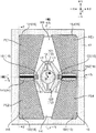
k1:接続セクション144のバネ係数
k2:トーションバー12のバネ係数
m1:ミラー枠13の慣性モーメント
m2:ミラー11の慣性モーメント
ωi:固有振動数
k11=k1+k2
k22=k2
k12=−k2
また、この構成によれば、第2の軸部を中心軸としてミラー枠を振動させる垂直走査時のミラーの慣性モーメントの変化を小さくすることが可能となり、垂直走査時の振動に悪い影響を与えることなく、ミラーの慣性モーメントを調節することが可能になる。
Claims (8)
- ミラーと、
第1の軸部と、
前記第1の軸部を介して前記ミラーを保持するミラー枠と、
前記ミラー枠を保持する第2の軸部と、
前記第2の軸部を介して前記ミラー枠に接続され、前記第2の軸部を中心軸として前記ミラー枠を振動させるとともに、振動する前記ミラー枠と前記第1の軸部とを介して前記第1の軸部を中心軸として前記ミラーを共振駆動することで、前記第1及び第2の軸部を中心軸として前記ミラーを振動させるアクチュエータとを備え、
前記第2の軸部は、変形可能な接続部を備え、前記接続部を介して前記アクチュエータに接続され、
前記ミラー枠は、前記アクチュエータの振動により前記第1の軸部を中心軸として振動することで前記ミラーを共振駆動させるときのミラー枠の慣性モーメントを増大させて前記アクチュエータの変位と前記ミラー枠の最大変位との差を減少させるための調整部材を、前記第2の軸部を中心軸とした振動が行われる際の前記ミラーの慣性モーメントの変化を小さくすべく、前記ミラー枠の振動の中心軸である前記第2の軸部の延長線上に備えることを特徴とする光スキャナ。 - 前記ミラー枠は、前記第1の軸部を中心として対称な重量を有し、
前記調整部材は、前記ミラー枠の重量が前記第1の軸部を中心に対称となるように設けられていることを特徴とする請求項1記載の光スキャナ。 - 前記第1の軸部の方向は、前記第2の軸部の方向に直交することを特徴とする請求項2記載の光スキャナ。
- 半導体材料により構成されたベース部を更に備え、
前記アクチュエータは、前記ベース部に貼り付けられた圧電素子の薄膜を含むユニモルフにより構成され、
前記調整部材は、前記圧電素子と同一材料の薄膜で構成され、
前記ミラー、前記第1の軸部、前記ミラー枠、及び前記第2の軸部は、前記半導体材料により構成されていることを特徴とする請求項1記載の光スキャナ。 - 前記ミラー枠の一部は、他の部分より厚く、
前記調整部材は、前記一部により構成されていることを特徴とする請求項1記載の光スキャナ。 - 前記ミラー枠は、前記第1の軸部を中心として左右対称、かつ、前記第2の軸部を中心として上下対称であって、前記ミラーを取り囲む形状を有していることを特徴とする請求項1記載の光スキャナ。
- 前記接続部は、前記第2の軸部の長手方向を長手方向とする複数のスリットを備えることを特徴とする請求項1記載の光スキャナ。
- 前記アクチュエータを取り囲む外枠を更に備え、
前記接続部は、前記ミラー枠を中心として左右一対の接続セクションにより構成され、
前記アクチュエータは、左側の接続セクションと前記外枠の上部との間に接続された左上アクチュエータと、左側の接続セクションと前記外枠の下部との間に接続された左下アクチュエータと、右側の接続セクションと前記外枠の上部との間に接続された右上アクチュエータと、前記右側の接続セクションと前記外枠の下部との間に接続された右下アクチュエータとを備えることを特徴とする請求項1記載の光スキャナ。
Priority Applications (1)
| Application Number | Priority Date | Filing Date | Title |
|---|---|---|---|
| JP2010530859A JP5423680B2 (ja) | 2008-09-25 | 2009-09-24 | 光スキャナ |
Applications Claiming Priority (4)
| Application Number | Priority Date | Filing Date | Title |
|---|---|---|---|
| JP2008245925 | 2008-09-25 | ||
| JP2008245925 | 2008-09-25 | ||
| PCT/JP2009/066557 WO2010035759A1 (ja) | 2008-09-25 | 2009-09-24 | 光スキャナ |
| JP2010530859A JP5423680B2 (ja) | 2008-09-25 | 2009-09-24 | 光スキャナ |
Publications (2)
| Publication Number | Publication Date |
|---|---|
| JPWO2010035759A1 JPWO2010035759A1 (ja) | 2012-02-23 |
| JP5423680B2 true JP5423680B2 (ja) | 2014-02-19 |
Family
ID=42059757
Family Applications (1)
| Application Number | Title | Priority Date | Filing Date |
|---|---|---|---|
| JP2010530859A Expired - Fee Related JP5423680B2 (ja) | 2008-09-25 | 2009-09-24 | 光スキャナ |
Country Status (4)
| Country | Link |
|---|---|
| US (1) | US8559089B2 (ja) |
| EP (1) | EP2330456A4 (ja) |
| JP (1) | JP5423680B2 (ja) |
| WO (1) | WO2010035759A1 (ja) |
Families Citing this family (14)
| Publication number | Priority date | Publication date | Assignee | Title |
|---|---|---|---|---|
| US8559089B2 (en) | 2008-09-25 | 2013-10-15 | Konica Minolta Opto, Inc. | Optical scanner |
| JP5333286B2 (ja) * | 2010-02-23 | 2013-11-06 | セイコーエプソン株式会社 | 光スキャナーおよび画像形成装置 |
| JP5381801B2 (ja) * | 2010-02-23 | 2014-01-08 | セイコーエプソン株式会社 | 画像形成装置 |
| CN101950079A (zh) * | 2010-05-26 | 2011-01-19 | 香港应用科技研究院有限公司 | 具有可调谐振频率的双轴扫描镜面 |
| DE102012201981B4 (de) * | 2012-02-10 | 2020-08-20 | Robert Bosch Gmbh | Mikromechanisches Bauteil und Herstellungsverfahren für ein mikromechanisches Bauteil |
| JP6988062B2 (ja) * | 2016-08-02 | 2022-01-05 | 株式会社リコー | 光偏向器、光走査装置、画像投影装置、画像形成装置、および移動体 |
| WO2018179589A1 (ja) | 2017-03-30 | 2018-10-04 | 三菱電機株式会社 | 光走査装置およびその製造方法 |
| EP3872556A4 (en) | 2018-10-25 | 2021-12-08 | FUJIFILM Corporation | MICROMIRROR DEVICE AND METHOD FOR DRIVING A MICROMIRROR DEVICE |
| CN109900221A (zh) * | 2019-04-12 | 2019-06-18 | 杭州思看科技有限公司 | 一种手持式三维扫描系统 |
| JP7354797B2 (ja) | 2019-11-27 | 2023-10-03 | 株式会社リコー | 光偏向器、偏向装置、距離測定装置、画像投影装置、及び車両 |
| JP7562469B2 (ja) * | 2021-04-13 | 2024-10-07 | 富士フイルム株式会社 | マイクロミラーデバイス及び光走査装置 |
| JP7667041B2 (ja) * | 2021-09-08 | 2025-04-22 | 富士フイルム株式会社 | マイクロミラーデバイス及び光走査装置 |
| JP7693475B2 (ja) | 2021-09-08 | 2025-06-17 | 富士フイルム株式会社 | マイクロミラーデバイス及び光走査装置 |
| WO2024261200A1 (de) * | 2023-06-20 | 2024-12-26 | OQmented GmbH | Mems-vorrichtung mit einer haltestruktur umfassend eine federstruktur, innere rahmenstruktur und/oder hebelstruktur |
Citations (7)
| Publication number | Priority date | Publication date | Assignee | Title |
|---|---|---|---|---|
| JP2005148459A (ja) * | 2003-11-17 | 2005-06-09 | Stanley Electric Co Ltd | 2次元光スキャナ及び光学装置 |
| JP2007199682A (ja) * | 2005-12-27 | 2007-08-09 | Konica Minolta Holdings Inc | 光偏向器および光ビーム走査装置 |
| JP2007310196A (ja) * | 2006-05-19 | 2007-11-29 | Konica Minolta Holdings Inc | 光スキャナ及び走査型プロジェクタ |
| JP2008020701A (ja) * | 2006-07-13 | 2008-01-31 | Stanley Electric Co Ltd | 2次元光スキャナ、それを用いた光学装置および2次元光スキャナの製造方法 |
| JP2008203299A (ja) * | 2007-02-16 | 2008-09-04 | Konica Minolta Opto Inc | マイクロスキャナおよびそれを備える光学機器 |
| JP2008254162A (ja) * | 2006-06-07 | 2008-10-23 | Canon Inc | 揺動体装置、光偏向器、及びそれを用いた光学機器 |
| JP2009098253A (ja) * | 2007-10-15 | 2009-05-07 | Panasonic Corp | 光学反射素子およびこれを用いた画像投影装置 |
Family Cites Families (5)
| Publication number | Priority date | Publication date | Assignee | Title |
|---|---|---|---|---|
| US7282775B2 (en) * | 2004-02-13 | 2007-10-16 | Advanced Numicro Systems, Inc. | MEMS scanning mirror with trenched surface and tapered comb teeth for reducing intertia and deformation |
| US7187488B2 (en) | 2005-03-09 | 2007-03-06 | Advanced Numicro Systems, Inc. | Trimming a MEMS device to fine tune natural frequency |
| US7557972B2 (en) | 2006-06-07 | 2009-07-07 | Canon Kabushiki Kaisha | Oscillator device, optical deflector and optical instrument using the same |
| US8559089B2 (en) | 2008-09-25 | 2013-10-15 | Konica Minolta Opto, Inc. | Optical scanner |
| US8072664B1 (en) * | 2010-05-26 | 2011-12-06 | Hong Kong Applied Science & Technology Research Institute, Ltd. | Biaxial scanning mirror having resonant frequency adjustment |
-
2009
- 2009-09-24 US US13/120,203 patent/US8559089B2/en not_active Expired - Fee Related
- 2009-09-24 EP EP09816174A patent/EP2330456A4/en not_active Withdrawn
- 2009-09-24 WO PCT/JP2009/066557 patent/WO2010035759A1/ja not_active Ceased
- 2009-09-24 JP JP2010530859A patent/JP5423680B2/ja not_active Expired - Fee Related
Patent Citations (7)
| Publication number | Priority date | Publication date | Assignee | Title |
|---|---|---|---|---|
| JP2005148459A (ja) * | 2003-11-17 | 2005-06-09 | Stanley Electric Co Ltd | 2次元光スキャナ及び光学装置 |
| JP2007199682A (ja) * | 2005-12-27 | 2007-08-09 | Konica Minolta Holdings Inc | 光偏向器および光ビーム走査装置 |
| JP2007310196A (ja) * | 2006-05-19 | 2007-11-29 | Konica Minolta Holdings Inc | 光スキャナ及び走査型プロジェクタ |
| JP2008254162A (ja) * | 2006-06-07 | 2008-10-23 | Canon Inc | 揺動体装置、光偏向器、及びそれを用いた光学機器 |
| JP2008020701A (ja) * | 2006-07-13 | 2008-01-31 | Stanley Electric Co Ltd | 2次元光スキャナ、それを用いた光学装置および2次元光スキャナの製造方法 |
| JP2008203299A (ja) * | 2007-02-16 | 2008-09-04 | Konica Minolta Opto Inc | マイクロスキャナおよびそれを備える光学機器 |
| JP2009098253A (ja) * | 2007-10-15 | 2009-05-07 | Panasonic Corp | 光学反射素子およびこれを用いた画像投影装置 |
Also Published As
| Publication number | Publication date |
|---|---|
| EP2330456A1 (en) | 2011-06-08 |
| US20110181933A1 (en) | 2011-07-28 |
| EP2330456A4 (en) | 2012-04-11 |
| US8559089B2 (en) | 2013-10-15 |
| JPWO2010035759A1 (ja) | 2012-02-23 |
| WO2010035759A1 (ja) | 2010-04-01 |
Similar Documents
| Publication | Publication Date | Title |
|---|---|---|
| JP5423680B2 (ja) | 光スキャナ | |
| JP7237146B2 (ja) | マイクロミラーデバイスおよびマイクロミラーデバイスの駆動方法 | |
| US8879132B2 (en) | Mirror driving apparatus, method of driving same and method of manufacturing same | |
| AU2007305711B2 (en) | Optical scanning device | |
| CN103827725B (zh) | 光学反射元件 | |
| JP5319939B2 (ja) | 光偏向器および光学装置 | |
| JP5915446B2 (ja) | 光走査装置 | |
| JP6024269B2 (ja) | 光走査装置 | |
| JP5853933B2 (ja) | 光走査装置および製造方法 | |
| US20120008185A1 (en) | Light beam scanning device | |
| JP2005128147A (ja) | 光偏向器及び光学装置 | |
| CN102695978A (zh) | 振动反射镜元件及振动反射镜元件的制造方法 | |
| JP7601961B2 (ja) | マイクロミラーデバイス | |
| US8804223B2 (en) | Light beam scanning device with a silicon mirror on a metal substrate | |
| JP7209082B2 (ja) | マイクロミラーデバイス | |
| JP4193817B2 (ja) | アクチュエータ | |
| JP5045470B2 (ja) | 光学反射素子 | |
| CN111149372B (zh) | 超声波传感器 | |
| JP2009223115A (ja) | 光学反射素子 | |
| JP5846097B2 (ja) | 光走査装置 | |
| JP2009217093A (ja) | 光学反射素子 | |
| JP2014202801A (ja) | 光学反射素子 | |
| JP5810685B2 (ja) | 振動子および振動ジャイロ | |
| JP2013003474A (ja) | マイクロスキャナ装置及び光学機器 | |
| JP2009223114A (ja) | 光学反射素子 |
Legal Events
| Date | Code | Title | Description |
|---|---|---|---|
| A621 | Written request for application examination |
Free format text: JAPANESE INTERMEDIATE CODE: A621 Effective date: 20120514 |
|
| A131 | Notification of reasons for refusal |
Free format text: JAPANESE INTERMEDIATE CODE: A131 Effective date: 20130409 |
|
| A711 | Notification of change in applicant |
Free format text: JAPANESE INTERMEDIATE CODE: A712 Effective date: 20130418 |
|
| A521 | Request for written amendment filed |
Free format text: JAPANESE INTERMEDIATE CODE: A523 Effective date: 20130607 |
|
| A02 | Decision of refusal |
Free format text: JAPANESE INTERMEDIATE CODE: A02 Effective date: 20130702 |
|
| A521 | Request for written amendment filed |
Free format text: JAPANESE INTERMEDIATE CODE: A523 Effective date: 20131001 |
|
| A911 | Transfer to examiner for re-examination before appeal (zenchi) |
Free format text: JAPANESE INTERMEDIATE CODE: A911 Effective date: 20131008 |
|
| TRDD | Decision of grant or rejection written | ||
| A01 | Written decision to grant a patent or to grant a registration (utility model) |
Free format text: JAPANESE INTERMEDIATE CODE: A01 Effective date: 20131029 |
|
| A61 | First payment of annual fees (during grant procedure) |
Free format text: JAPANESE INTERMEDIATE CODE: A61 Effective date: 20131111 |
|
| R150 | Certificate of patent or registration of utility model |
Free format text: JAPANESE INTERMEDIATE CODE: R150 |
|
| LAPS | Cancellation because of no payment of annual fees |