JP5500833B2 - Soi基板の作製方法 - Google Patents
Soi基板の作製方法 Download PDFInfo
- Publication number
- JP5500833B2 JP5500833B2 JP2009022151A JP2009022151A JP5500833B2 JP 5500833 B2 JP5500833 B2 JP 5500833B2 JP 2009022151 A JP2009022151 A JP 2009022151A JP 2009022151 A JP2009022151 A JP 2009022151A JP 5500833 B2 JP5500833 B2 JP 5500833B2
- Authority
- JP
- Japan
- Prior art keywords
- oxide film
- substrate
- film
- single crystal
- base substrate
- Prior art date
- Legal status (The legal status is an assumption and is not a legal conclusion. Google has not performed a legal analysis and makes no representation as to the accuracy of the status listed.)
- Expired - Fee Related
Links
Images




Classifications
-
- H—ELECTRICITY
- H10—SEMICONDUCTOR DEVICES; ELECTRIC SOLID-STATE DEVICES NOT OTHERWISE PROVIDED FOR
- H10D—INORGANIC ELECTRIC SEMICONDUCTOR DEVICES
- H10D86/00—Integrated devices formed in or on insulating or conducting substrates, e.g. formed in silicon-on-insulator [SOI] substrates or on stainless steel or glass substrates
- H10D86/01—Manufacture or treatment
- H10D86/021—Manufacture or treatment of multiple TFTs
- H10D86/0214—Manufacture or treatment of multiple TFTs using temporary substrates
-
- H—ELECTRICITY
- H10—SEMICONDUCTOR DEVICES; ELECTRIC SOLID-STATE DEVICES NOT OTHERWISE PROVIDED FOR
- H10D—INORGANIC ELECTRIC SEMICONDUCTOR DEVICES
- H10D86/00—Integrated devices formed in or on insulating or conducting substrates, e.g. formed in silicon-on-insulator [SOI] substrates or on stainless steel or glass substrates
- H10D86/40—Integrated devices formed in or on insulating or conducting substrates, e.g. formed in silicon-on-insulator [SOI] substrates or on stainless steel or glass substrates characterised by multiple TFTs
-
- H—ELECTRICITY
- H10—SEMICONDUCTOR DEVICES; ELECTRIC SOLID-STATE DEVICES NOT OTHERWISE PROVIDED FOR
- H10D—INORGANIC ELECTRIC SEMICONDUCTOR DEVICES
- H10D86/00—Integrated devices formed in or on insulating or conducting substrates, e.g. formed in silicon-on-insulator [SOI] substrates or on stainless steel or glass substrates
- H10D86/40—Integrated devices formed in or on insulating or conducting substrates, e.g. formed in silicon-on-insulator [SOI] substrates or on stainless steel or glass substrates characterised by multiple TFTs
- H10D86/60—Integrated devices formed in or on insulating or conducting substrates, e.g. formed in silicon-on-insulator [SOI] substrates or on stainless steel or glass substrates characterised by multiple TFTs wherein the TFTs are in active matrices
-
- H—ELECTRICITY
- H10—SEMICONDUCTOR DEVICES; ELECTRIC SOLID-STATE DEVICES NOT OTHERWISE PROVIDED FOR
- H10P—GENERIC PROCESSES OR APPARATUS FOR THE MANUFACTURE OR TREATMENT OF DEVICES COVERED BY CLASS H10
- H10P90/00—Preparation of wafers not covered by a single main group of this subclass, e.g. wafer reinforcement
- H10P90/19—Preparing inhomogeneous wafers
- H10P90/1904—Preparing vertically inhomogeneous wafers
- H10P90/1906—Preparing SOI wafers
- H10P90/1914—Preparing SOI wafers using bonding
- H10P90/1916—Preparing SOI wafers using bonding with separation or delamination along an ion implanted layer, e.g. Smart-cut
-
- H—ELECTRICITY
- H10—SEMICONDUCTOR DEVICES; ELECTRIC SOLID-STATE DEVICES NOT OTHERWISE PROVIDED FOR
- H10W—GENERIC PACKAGES, INTERCONNECTIONS, CONNECTORS OR OTHER CONSTRUCTIONAL DETAILS OF DEVICES COVERED BY CLASS H10
- H10W10/00—Isolation regions in semiconductor bodies between components of integrated devices
- H10W10/10—Isolation regions comprising dielectric materials
- H10W10/181—Semiconductor-on-insulator [SOI] isolation regions, e.g. buried oxide regions of SOI wafers
-
- H—ELECTRICITY
- H10—SEMICONDUCTOR DEVICES; ELECTRIC SOLID-STATE DEVICES NOT OTHERWISE PROVIDED FOR
- H10D—INORGANIC ELECTRIC SEMICONDUCTOR DEVICES
- H10D30/00—Field-effect transistors [FET]
- H10D30/01—Manufacture or treatment
- H10D30/021—Manufacture or treatment of FETs having insulated gates [IGFET]
- H10D30/031—Manufacture or treatment of FETs having insulated gates [IGFET] of thin-film transistors [TFT]
- H10D30/0321—Manufacture or treatment of FETs having insulated gates [IGFET] of thin-film transistors [TFT] comprising silicon, e.g. amorphous silicon or polysilicon
- H10D30/0323—Manufacture or treatment of FETs having insulated gates [IGFET] of thin-film transistors [TFT] comprising silicon, e.g. amorphous silicon or polysilicon comprising monocrystalline silicon
Landscapes
- Thin Film Transistor (AREA)
- Liquid Crystal (AREA)
- Electroluminescent Light Sources (AREA)
- Metal-Oxide And Bipolar Metal-Oxide Semiconductor Integrated Circuits (AREA)
- Recrystallisation Techniques (AREA)
- Element Separation (AREA)
Description
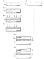
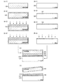
本実施の形態では、半導体基板とベース基板を貼り合わせてSOI基板を作製する方法に関して図面を参照して説明する。
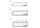
本実施の形態では、上記実施の形態と異なるSOI基板の作製方法に関して図面を参照して説明する。具体的には、ベース基板の表面に絶縁膜を形成する場合について説明する。
本実施の形態では、上記実施の形態で作製したSOI基板を用いて、半導体装置を作製する方法を説明する。
102 酸化膜
103 イオン
104 脆化領域
112 酸化膜
120 ベース基板
121 半導体膜
122 酸化膜
124 単結晶半導体膜
251 半導体膜
252 半導体膜
254 絶縁膜
255 ゲート電極
256 ゲート電極
257 低濃度不純物領域
258 チャネル形成領域
259 高濃度不純物領域
260 チャネル形成領域
261 サイドウォール絶縁膜
265 レジスト
267 高濃度不純物領域
268 絶縁膜
269 層間絶縁膜
270 配線
302 単結晶半導体膜
320 単結晶半導体膜
322 走査線
323 信号線
324 画素電極
325 TFT
327 層間絶縁膜
328 電極
329 柱状スペーサ
330 配向膜
332 対向基板
333 対向電極
334 配向膜
335 液晶層
340 チャネル形成領域
341 高濃度不純物領域
401 選択用トランジスタ
402 表示制御用トランジスタ
403 半導体膜
404 半導体膜
405 走査線
406 信号線
407 電流供給線
408 画素電極
410 電極
411 電極
412 ゲート電極
413 電極
427 層間絶縁膜
428 隔壁層
429 EL層
430 対向電極
431 対向基板
432 樹脂層
451 チャネル形成領域
452 高濃度不純物領域
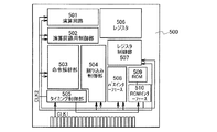
500 マイクロプロセッサ
501 演算回路
502 演算回路制御部
503 命令解析部
504 制御部
505 タイミング制御部
506 レジスタ
507 レジスタ制御部
508 バスインターフェース
509 専用メモリ
510 メモリインターフェース
511 RFCPU
512 アナログ回路部
513 デジタル回路部
514 共振回路
515 整流回路
516 定電圧回路
517 リセット回路
518 発振回路
519 復調回路
520 変調回路
521 RFインターフェース
522 制御レジスタ
523 クロックコントローラ
524 インターフェース
525 中央処理ユニット
526 ランダムアクセスメモリ
527 専用メモリ
528 アンテナ
529 容量部
530 電源管理回路
550 加熱温度
700 携帯電話
701 筐体
702 筐体
703 表示部
704 スピーカ
705 マイクロフォン
706 操作キー
707 ポインティングデバイス
708 表面カメラ用レンズ
709 外部接続端子ジャック
710 イヤホン端子
711 キーボード
712 外部メモリスロット
713 裏面カメラ
714 ライト
Claims (5)
- 塩化水素を含有させた酸化性雰囲気で単結晶半導体基板に熱酸化処理を行い、前記単結晶半導体基板上に塩素原子を含有する第1の酸化膜を形成し、
絶縁体からなるベース基板上に半導体膜を形成し、
トランス−1,2−ジクロロエチレンを含有させた酸化性雰囲気で熱酸化処理を行い、前記半導体膜を酸化させ、塩素原子を含有する第3の酸化膜を形成し、
前記第1の酸化膜を介して前記単結晶半導体基板に加速されたイオンを照射することにより、前記単結晶半導体基板の表面から所定の深さの領域に脆化領域を形成し、
バイアス電圧を印加して、前記単結晶半導体基板上の前記第1の酸化膜に対して酸素ガスを用いたプラズマ処理を行って、第2の酸化膜とし、
前記単結晶半導体基板と前記ベース基板とを対向させ、前記第2の酸化膜の表面と前記第3の酸化膜の表面とを接合させ、
前記第2の酸化膜の表面と前記第3の酸化膜の表面とを接合させた後に熱処理を行い、前記脆化領域において分離することにより、前記ベース基板上に前記第3の酸化膜及び前記第2の酸化膜を介して単結晶半導体膜を形成することを特徴とするSOI基板の作製方法。 - 請求項1において、
前記第2の酸化膜の表面と前記第3の酸化膜の表面とを接合させる前に、バイアス電圧を印加して、前記ベース基板上の前記第3の酸化膜に対してプラズマ処理を行うことを特徴とするSOI基板の作製方法。 - 請求項1又は請求項2において、
前記第2の酸化膜は、前記第2の酸化膜と前記単結晶半導体膜の界面側における前記塩素原子の濃度が高く、前記第2の酸化膜と前記ベース基板の界面側における前記塩素原子の濃度が低いことを特徴とするSOI基板の作製方法。 - 請求項1乃至請求項3のいずれか一項において、
前記熱処理は、ベース基板の歪点以下の温度で行うことを特徴とするSOI基板の作製方法。 - 請求項1乃至請求項4のいずれか一項において、
前記ベース基板として、ガラス基板を用いることを特徴とするSOI基板の作製方法。
Priority Applications (1)
| Application Number | Priority Date | Filing Date | Title |
|---|---|---|---|
| JP2009022151A JP5500833B2 (ja) | 2008-02-04 | 2009-02-03 | Soi基板の作製方法 |
Applications Claiming Priority (3)
| Application Number | Priority Date | Filing Date | Title |
|---|---|---|---|
| JP2008024520 | 2008-02-04 | ||
| JP2008024520 | 2008-02-04 | ||
| JP2009022151A JP5500833B2 (ja) | 2008-02-04 | 2009-02-03 | Soi基板の作製方法 |
Publications (3)
| Publication Number | Publication Date |
|---|---|
| JP2009212502A JP2009212502A (ja) | 2009-09-17 |
| JP2009212502A5 JP2009212502A5 (ja) | 2012-02-02 |
| JP5500833B2 true JP5500833B2 (ja) | 2014-05-21 |
Family
ID=40939235
Family Applications (1)
| Application Number | Title | Priority Date | Filing Date |
|---|---|---|---|
| JP2009022151A Expired - Fee Related JP5500833B2 (ja) | 2008-02-04 | 2009-02-03 | Soi基板の作製方法 |
Country Status (4)
| Country | Link |
|---|---|
| US (1) | US8119490B2 (ja) |
| JP (1) | JP5500833B2 (ja) |
| CN (1) | CN101510524B (ja) |
| TW (1) | TWI494974B (ja) |
Families Citing this family (12)
| Publication number | Priority date | Publication date | Assignee | Title |
|---|---|---|---|---|
| JP5663150B2 (ja) * | 2008-07-22 | 2015-02-04 | 株式会社半導体エネルギー研究所 | Soi基板の作製方法 |
| JP4333820B1 (ja) * | 2009-01-19 | 2009-09-16 | 住友電気工業株式会社 | 化合物半導体基板 |
| WO2011070892A1 (en) * | 2009-12-08 | 2011-06-16 | Semiconductor Energy Laboratory Co., Ltd. | Semiconductor device and manufacturing method thereof |
| US9299852B2 (en) * | 2011-06-16 | 2016-03-29 | Semiconductor Energy Laboratory Co., Ltd. | Semiconductor device and method for manufacturing the same |
| CN102569501B (zh) * | 2011-12-15 | 2014-06-18 | 苏州阿特斯阳光电力科技有限公司 | 一种多晶硅太阳能电池的磷扩散方法 |
| CN104040686B (zh) * | 2012-01-12 | 2017-05-24 | 信越化学工业株式会社 | 热氧化异种复合基板及其制造方法 |
| TWI669835B (zh) | 2012-07-05 | 2019-08-21 | 日商半導體能源研究所股份有限公司 | 發光裝置 |
| KR102173801B1 (ko) | 2012-07-12 | 2020-11-04 | 가부시키가이샤 한도오따이 에네루기 켄큐쇼 | 표시 장치, 및 표시 장치의 제작 방법 |
| CN105448657A (zh) * | 2014-09-02 | 2016-03-30 | 无锡华润上华半导体有限公司 | 一种改善高压器件阈值电压均匀性的方法 |
| CN104952791A (zh) * | 2015-06-26 | 2015-09-30 | 深圳市华星光电技术有限公司 | Amoled显示器件的制作方法及其结构 |
| US11289330B2 (en) | 2019-09-30 | 2022-03-29 | Taiwan Semiconductor Manufacturing Company, Ltd. | Semiconductor-on-insulator (SOI) substrate and method for forming |
| CN114188270B (zh) * | 2021-12-09 | 2024-11-22 | 北京工业大学 | 一种基于基质面化学反应的固体薄膜剥离方法 |
Family Cites Families (18)
| Publication number | Priority date | Publication date | Assignee | Title |
|---|---|---|---|---|
| JPH0254532A (ja) | 1988-08-17 | 1990-02-23 | Sony Corp | Soi基板の製造方法 |
| US5362667A (en) * | 1992-07-28 | 1994-11-08 | Harris Corporation | Bonded wafer processing |
| KR970052022A (ko) * | 1995-12-30 | 1997-07-29 | 김주용 | 에스 오 아이 기판 제조방법 |
| JPH10284431A (ja) * | 1997-04-11 | 1998-10-23 | Sharp Corp | Soi基板の製造方法 |
| US6534380B1 (en) * | 1997-07-18 | 2003-03-18 | Denso Corporation | Semiconductor substrate and method of manufacturing the same |
| JPH11163363A (ja) * | 1997-11-22 | 1999-06-18 | Semiconductor Energy Lab Co Ltd | 半導体装置およびその作製方法 |
| JP2000124092A (ja) | 1998-10-16 | 2000-04-28 | Shin Etsu Handotai Co Ltd | 水素イオン注入剥離法によってsoiウエーハを製造する方法およびこの方法で製造されたsoiウエーハ |
| CN1118087C (zh) * | 1999-09-27 | 2003-08-13 | 中国科学院半导体研究所 | 一种制备半导体衬底的方法 |
| US6737337B1 (en) * | 2001-04-27 | 2004-05-18 | Advanced Micro Devices, Inc. | Method of preventing dopant depletion in surface semiconductor layer of semiconductor-on-insulator (SOI) device |
| US20030134486A1 (en) * | 2002-01-16 | 2003-07-17 | Zhongze Wang | Semiconductor-on-insulator comprising integrated circuitry |
| US7119365B2 (en) | 2002-03-26 | 2006-10-10 | Sharp Kabushiki Kaisha | Semiconductor device and manufacturing method thereof, SOI substrate and display device using the same, and manufacturing method of the SOI substrate |
| JP4772258B2 (ja) | 2002-08-23 | 2011-09-14 | シャープ株式会社 | Soi基板の製造方法 |
| US7109092B2 (en) | 2003-05-19 | 2006-09-19 | Ziptronix, Inc. | Method of room temperature covalent bonding |
| US20070110917A1 (en) * | 2003-12-02 | 2007-05-17 | Bondtech, Inc | Bonding method, device formed by such method, surface activating unit and bonding apparatus comprising such unit |
| FR2868599B1 (fr) * | 2004-03-30 | 2006-07-07 | Soitec Silicon On Insulator | Traitement chimique optimise de type sc1 pour le nettoyage de plaquettes en materiau semiconducteur |
| US7148124B1 (en) * | 2004-11-18 | 2006-12-12 | Alexander Yuri Usenko | Method for forming a fragile layer inside of a single crystalline substrate preferably for making silicon-on-insulator wafers |
| FR2884966B1 (fr) * | 2005-04-22 | 2007-08-17 | Soitec Silicon On Insulator | Procede de collage de deux tranches realisees dans des materiaux choisis parmi les materiaux semiconducteurs |
| FR2888663B1 (fr) * | 2005-07-13 | 2008-04-18 | Soitec Silicon On Insulator | Procede de diminution de la rugosite d'une couche epaisse d'isolant |
-
2009
- 2009-01-12 US US12/352,176 patent/US8119490B2/en not_active Expired - Fee Related
- 2009-02-02 TW TW098103240A patent/TWI494974B/zh not_active IP Right Cessation
- 2009-02-03 JP JP2009022151A patent/JP5500833B2/ja not_active Expired - Fee Related
- 2009-02-04 CN CN2009100057935A patent/CN101510524B/zh not_active Expired - Fee Related
Also Published As
| Publication number | Publication date |
|---|---|
| CN101510524A (zh) | 2009-08-19 |
| TW200943387A (en) | 2009-10-16 |
| US20090203191A1 (en) | 2009-08-13 |
| CN101510524B (zh) | 2013-07-24 |
| JP2009212502A (ja) | 2009-09-17 |
| US8119490B2 (en) | 2012-02-21 |
| TWI494974B (zh) | 2015-08-01 |
Similar Documents
| Publication | Publication Date | Title |
|---|---|---|
| JP5500833B2 (ja) | Soi基板の作製方法 | |
| JP5548395B2 (ja) | Soi基板の作製方法 | |
| JP5568260B2 (ja) | Soi基板の作製方法 | |
| US8143134B2 (en) | Method for manufacturing SOI substrate | |
| JP5663150B2 (ja) | Soi基板の作製方法 | |
| JP5478166B2 (ja) | 半導体装置の作製方法 | |
| JP2009212503A (ja) | Soi基板の作製方法 | |
| JP2010114431A (ja) | Soi基板の作製方法 | |
| JP5667767B2 (ja) | Soi基板の作製方法 | |
| JP5666794B2 (ja) | Soi基板の作製方法 | |
| JP5386193B2 (ja) | Soi基板の作製方法 | |
| JP5618521B2 (ja) | 半導体装置の作製方法 | |
| JP2010177662A (ja) | Soi基板の作製方法及び半導体装置の作製方法 | |
| JP5580010B2 (ja) | 半導体装置の作製方法 | |
| JP5841725B2 (ja) | Soi基板の作製方法 | |
| JP2010147313A (ja) | Soi基板の作製方法 |
Legal Events
| Date | Code | Title | Description |
|---|---|---|---|
| A521 | Request for written amendment filed |
Free format text: JAPANESE INTERMEDIATE CODE: A821 Effective date: 20111129 |
|
| RD02 | Notification of acceptance of power of attorney |
Free format text: JAPANESE INTERMEDIATE CODE: A7422 Effective date: 20111129 |
|
| A521 | Request for written amendment filed |
Free format text: JAPANESE INTERMEDIATE CODE: A523 Effective date: 20111207 |
|
| A621 | Written request for application examination |
Free format text: JAPANESE INTERMEDIATE CODE: A621 Effective date: 20111207 |
|
| A977 | Report on retrieval |
Free format text: JAPANESE INTERMEDIATE CODE: A971007 Effective date: 20130926 |
|
| A131 | Notification of reasons for refusal |
Free format text: JAPANESE INTERMEDIATE CODE: A131 Effective date: 20131001 |
|
| TRDD | Decision of grant or rejection written | ||
| A01 | Written decision to grant a patent or to grant a registration (utility model) |
Free format text: JAPANESE INTERMEDIATE CODE: A01 Effective date: 20140225 |
|
| A61 | First payment of annual fees (during grant procedure) |
Free format text: JAPANESE INTERMEDIATE CODE: A61 Effective date: 20140311 |
|
| R150 | Certificate of patent or registration of utility model |
Ref document number: 5500833 Country of ref document: JP Free format text: JAPANESE INTERMEDIATE CODE: R150 |
|
| R250 | Receipt of annual fees |
Free format text: JAPANESE INTERMEDIATE CODE: R250 |
|
| LAPS | Cancellation because of no payment of annual fees |