JP5500907B2 - 半導体装置およびその製造方法 - Google Patents
半導体装置およびその製造方法 Download PDFInfo
- Publication number
- JP5500907B2 JP5500907B2 JP2009191589A JP2009191589A JP5500907B2 JP 5500907 B2 JP5500907 B2 JP 5500907B2 JP 2009191589 A JP2009191589 A JP 2009191589A JP 2009191589 A JP2009191589 A JP 2009191589A JP 5500907 B2 JP5500907 B2 JP 5500907B2
- Authority
- JP
- Japan
- Prior art keywords
- manufacturing
- film
- wiring
- semiconductor device
- conductive film
- Prior art date
- Legal status (The legal status is an assumption and is not a legal conclusion. Google has not performed a legal analysis and makes no representation as to the accuracy of the status listed.)
- Expired - Fee Related
Links
Images







Classifications
-
- H—ELECTRICITY
- H10—SEMICONDUCTOR DEVICES; ELECTRIC SOLID-STATE DEVICES NOT OTHERWISE PROVIDED FOR
- H10D—INORGANIC ELECTRIC SEMICONDUCTOR DEVICES
- H10D30/00—Field-effect transistors [FET]
- H10D30/60—Insulated-gate field-effect transistors [IGFET]
- H10D30/67—Thin-film transistors [TFT]
- H10D30/674—Thin-film transistors [TFT] characterised by the active materials
- H10D30/6755—Oxide semiconductors, e.g. zinc oxide, copper aluminium oxide or cadmium stannate
-
- H—ELECTRICITY
- H10—SEMICONDUCTOR DEVICES; ELECTRIC SOLID-STATE DEVICES NOT OTHERWISE PROVIDED FOR
- H10D—INORGANIC ELECTRIC SEMICONDUCTOR DEVICES
- H10D30/00—Field-effect transistors [FET]
- H10D30/01—Manufacture or treatment
- H10D30/021—Manufacture or treatment of FETs having insulated gates [IGFET]
- H10D30/031—Manufacture or treatment of FETs having insulated gates [IGFET] of thin-film transistors [TFT]
-
- H—ELECTRICITY
- H10—SEMICONDUCTOR DEVICES; ELECTRIC SOLID-STATE DEVICES NOT OTHERWISE PROVIDED FOR
- H10D—INORGANIC ELECTRIC SEMICONDUCTOR DEVICES
- H10D86/00—Integrated devices formed in or on insulating or conducting substrates, e.g. formed in silicon-on-insulator [SOI] substrates or on stainless steel or glass substrates
- H10D86/01—Manufacture or treatment
- H10D86/021—Manufacture or treatment of multiple TFTs
- H10D86/0231—Manufacture or treatment of multiple TFTs using masks, e.g. half-tone masks
-
- H—ELECTRICITY
- H10—SEMICONDUCTOR DEVICES; ELECTRIC SOLID-STATE DEVICES NOT OTHERWISE PROVIDED FOR
- H10D—INORGANIC ELECTRIC SEMICONDUCTOR DEVICES
- H10D86/00—Integrated devices formed in or on insulating or conducting substrates, e.g. formed in silicon-on-insulator [SOI] substrates or on stainless steel or glass substrates
- H10D86/40—Integrated devices formed in or on insulating or conducting substrates, e.g. formed in silicon-on-insulator [SOI] substrates or on stainless steel or glass substrates characterised by multiple TFTs
- H10D86/60—Integrated devices formed in or on insulating or conducting substrates, e.g. formed in silicon-on-insulator [SOI] substrates or on stainless steel or glass substrates characterised by multiple TFTs wherein the TFTs are in active matrices
Landscapes
- Thin Film Transistor (AREA)
- Liquid Crystal (AREA)
- Electrodes Of Semiconductors (AREA)
Description
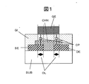
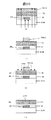
図2に、酸化物半導体を用い作成したトップゲート、ボトムコンタクト型のTFTを示す。ここでいうトップゲートとは、チャネル層CHNよりも上層にゲート電極GEが形成されている構造のことであり、ボトムコンタクトとは、チャネル層CHNよりも下層にソース電極SEおよびドレイン電極DEが形成されている構造のことである。
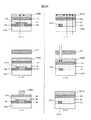
導電層CLを形成する。導電層CLの成膜はCVD法やスパッタ法などにより行ない、加工は一般的なフォトリソグラフィー技術とドライエッチングとの組み合わせにより行なう。
図11は、本実施の形態2における半導体装置の構成および製造方法を示す図である。半導体装置としていわゆるトップゲート/トップコンタクト型酸化物TFTを挙げている。ここでいうトップゲートとは、チャネル層CHNよりも上層にゲート電極GEが形成されている構造のことであり、トップコンタクトとは、チャネル層CHNよりも上層にソース電極SEおよびドレイン電極DEが形成されている構造のことを示している。
図12は、本実施の形態3における半導体装置の構成および製造方法を示す図である。半導体装置としていわゆるボトムゲート/トップコンタクト型酸化物TFTを挙げている。ここでいうボトムゲートとは、チャネル層CHNよりも下層にゲート電極GEが形成されている構造のことであり、トップコンタクトとは、チャネル層CHNよりも上層にソース電極SEおよびドレイン電極DEが形成されている構造のことを示している。
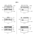
図17は、本実施の形態4における半導体装置の構成および製造方法を示す図である。半導体装置としていわゆるボトムゲート/ボトムコンタクト型酸化物TFTを挙げている。ここでいうボトムゲートとは、チャネル層CHNよりも下層にゲート電極GEが形成されている構造のことであり、ボトムコンタクトとは、チャネル層CHNよりも下層にソース電極SEおよびドレイン電極DEが形成されている構造のことを示している。
図18は、本実施の形態5における半導体装置の構成および製造方法を示す図である。半導体装置としていわゆるボトムゲート型酸化物TFTを挙げている。ここでいうボトムゲートとは、チャネル層CHNよりも下層にゲート電極GEが形成されている構造のことを示している。
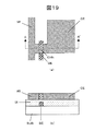
図20は、本実施の形態6における半導体装置の構成および製造方法を示す図である。半導体装置としていわゆるボトムゲート型酸化物TFTを挙げている。ここでいうボトムゲートとは、チャネル層CHNよりも下層にゲート電極GEが形成されている構造のことを示している。
図21は本実施の形態5における半導体装置の構成を示す図である。実施の形態1〜6に示す構造の酸化物TFTを用いてアンテナ共振回路AR、整流器RCT、変調器MOD、デジタル回路DGCなどを構成し、無線タグを形成している。無線タグはリーダRDまたはライタWRと無線で通信を行うことができるようになっている。無線タグでは、リーダRDやライタWRとの無線通信を行なうが、高周波での動作が要求される。このとき、前記実施の形態1〜6に示す自己整合型酸化物TFTでは、寄生容量が小さいため高周波での動作が可能になる。これにより、前記実施の形態1〜6における自己整合型酸化物TFTを使用した回路の高速化を図ることができる。このことから、前記実施の形態1〜6に示す自己整合型酸化物TFTは、高周波動作が必要とされる無線タグの使用に適しているといえる。
図22は本実施の形態8における半導体装置の構成を示す図である。本実施の形態8では、前記実施の形態1〜6の構造を有する酸化物TFTを構成要素とする素子が基板SUB上にアレイ状に配置されている。前記実施の形態1〜6に示す酸化物TFTを、アレイ内の各素子のスイッチングや駆動用のトランジスタに用いることはもちろん、この酸化物TFTのゲート電極GEと接続されるゲート線GLに信号を送るゲート線駆動回路GDCや、この酸化物TFTのソース電極SEあるいはドレイン電極DEと接続されるデータ線DLに信号を送るデータ線駆動回路DDCを構成するトランジスタに用いてもよい。この場合、各素子の酸化物TFTとゲート線駆動回路GDCあるいはデータ線駆動回路DDC内の酸化物TFTを並行して形成することができる。
CE 容量電極
CHN チャネル層
CHN2 チャネル層
CP 寄生容量
DDC データ線駆動回路
DE ドレイン電極
DE2 ドレイン電極
DGC デジタル回路
DL データ線
GDC ゲート線駆動回路
GE ゲート電極
GE2 ゲート電極
GI ゲート絶縁膜
GL ゲート線
IF 絶縁膜
LWI 下層配線
MOD 変調器
NRES ネガレジスト
OL オーバラップ
PE 画素電極
PM フォトマスク
PRES ポジレジスト
RCT 整流器
RD リーダ
SE ソース電極
SE2 ソース電極
SUB 基板
TCL 透明導電膜
TFT 酸化物TFT
UWI 上層配線
WI 配線
WR ライタ
Claims (16)
- 基板上に金属膜によりソース電極とドレイン電極と共に第1配線を形成し、酸化物半導体によりチャネル膜を形成し、
前記ソース電極と前記ドレイン電極と前記チャネル膜の上にゲート絶縁膜を形成し、
前記ゲート絶縁膜上に、導電膜を形成し、
前記導電膜上にネガレジストを塗布し、
前記ソース電極と前記ドレイン電極と共に前記第1配線をマスクとして、前記基板の裏面側から前記ネガレジストを露光し、
前記ネガレジストの露光部分を残し前記ネガレジストを除去し、
前記露光部分をエッチングマスクとして前記導電膜をエッチングし、
前記導電膜上にレジストを塗布し、
前記基板の表面側から前記レジストを露光し、
露光後の前記レジストをエッチングマスクとして前記導電膜を再度エッチングすることで、ゲート電極と共に第2配線を形成し、
前記第1配線直上の前記第2配線の分断部分に第3配線を形成し接続することを特徴とする半導体装置の製造方法。 - 請求項1記載の製造方法において、
前記裏面露光の光源として、水銀ランプのi線を用いることを特徴とする半導体装置の製造方法。 - 請求項1記載の製造方法において、
前記基板は、プラスチックフィルムからなることを特徴とする半導体装置の製造方法。 - 請求項1記載の製造方法において、
前記チャネル膜は、Zn−O、In-O、Ga-O、Sn-O、In−Ga−Zn−O、Zn−Sn−O、In−Sn−O、In−Zn−O、Ga−Zn−O、In−Ga−Oの何れか一つから成ることを特徴とする半導体装置の製造方法。 - 請求項1記載の製造方法において、
前記ゲート絶縁膜は、Si−O、Al−O、Si−Nの何れか一つから成ることを特徴とする半導体装置の製造方法。 - 請求項1記載の製造方法において、
前記導電膜は、In-Sn-O、Al−Zn-O、Sn−Oの何れか一つから成ることを特徴とする半導体装置の製造方法。 - 請求項1記載の製造方法において、
前記基板と、チャネル膜と、ゲート絶縁膜と、導電膜は透明であり、
前記金属膜は不透明であることを特徴とする半導体装置の製造方法。 - 基板上に金属膜によりゲート電極と共に第1配線を形成し、
前記ゲート電極と前記基板の上にゲート絶縁膜を形成し、
前記ゲート絶縁膜上に酸化物半導体によりチャネル膜を形成し、
前記チャネル膜上に導電膜を形成し、
前記導電膜上にネガレジストを塗布し、
前記ゲート電極と共に前記第1配線をマスクとして、前記基板の裏面側から前記ネガレジストを露光し、
前記ネガレジストの露光部分を残し前記ネガレジストを除去し、
前記露光部分をエッチングマスクとして前記導電膜をエッチングし、
前記導電膜上にレジストを塗布し、
前記基板の表面側から前記レジストを露光し、
露光後の前記レジストをエッチングマスクとして前記導電膜を再度エッチングすることで、ソース電極とドレイン電極と共に第2配線を形成し、
前記第1配線直上の前記第2配線の分断部分に第3配線を形成し接続することを特徴とする半導体装置の製造方法。 - 請求項8記載の製造方法において、
前記裏面露光の光源として、水銀ランプのi線を用いることを特徴とする半導体装置の製造方法。 - 請求項8記載の製造方法において、
前記基板は、プラスチックフィルムからなることを特徴とする半導体装置の製造方法。 - 請求項8記載の製造方法において、
前記チャネル膜は、Zn−O、In-O、Ga-O、Sn-O、In−Ga−Zn−O、Zn−Sn−O、In−Sn−O、In−Zn−O、Ga−Zn−O、In−Ga−Oの何れか一つから成ることを特徴とする半導体装置の製造方法。 - 請求項8記載の製造方法において、
前記ゲート絶縁膜は、Si−O、Al−O、Si−Nの何れか一つから成ることを特徴とする半導体装置の製造方法。 - 請求項8記載の製造方法において、
前記導電膜は、In-Sn-O、Al−Zn-O、Sn−Oの何れか一つから成ることを特徴とする半導体装置の製造方法。 - 請求項8記載の製造方法において、
前記基板と、チャネル膜と、ゲート絶縁膜と、導電膜は透明であり、
前記金属膜は不透明であることを特徴とする半導体装置の製造方法。 - 基板上に金属膜によりソース電極とドレイン電極と共に第1配線を形成し、酸化物半導体によりチャネル膜を形成し、
前記ソース電極と前記ドレイン電極と前記チャネル膜の上にゲート絶縁膜を形成し、
前記ゲート絶縁膜上に、導電膜を形成し、
前記導電膜上にネガレジストを塗布し、
前記ソース電極と前記ドレイン電極と共に前記第1配線をマスクとして、前記基板の裏面側から前記ネガレジストを露光し、
前記ネガレジストの露光部分を残し前記ネガレジストを除去し、
前記露光部分をエッチングマスクとして前記導電膜をエッチングし、
前記導電膜上にレジストを塗布し、
前記基板の表面側から前記レジストを露光し、
露光後の前記レジストをエッチングマスクとする前記導電膜のエッチングにより、ゲート電極と共に第2配線を形成し、
前記第1配線直上の前記第2配線の分断部分に第3配線を形成し接続することにより製造された半導体装置。 - 基板上に金属膜によりゲート電極と共に第1配線を形成し、
前記ゲート電極と前記基板の上にゲート絶縁膜を形成し、
前記ゲート絶縁膜上に酸化物半導体によりチャネル膜を形成し、
前記チャネル膜上に導電膜を形成し、
前記導電膜上にネガレジストを塗布し、
前記ゲート電極と共に前記第1配線をマスクとして、前記基板の裏面側から前記ネガレジストを露光し、
前記ネガレジストの露光部分を残し前記ネガレジストを除去し、
前記露光部分をエッチングマスクとして前記導電膜をエッチングし、
前記導電膜上にレジストを塗布し、
前記基板の表面側から前記レジストを露光し、
露光後の前記レジストをエッチングマスクとして前記導電膜を再度エッチングすることで、ソース電極とドレイン電極と共に第2配線を形成し、
前記第1配線直上の前記第2配線の分断部分に第3配線を形成し接続することにより製造された半導体装置。
Priority Applications (3)
| Application Number | Priority Date | Filing Date | Title |
|---|---|---|---|
| JP2009191589A JP5500907B2 (ja) | 2009-08-21 | 2009-08-21 | 半導体装置およびその製造方法 |
| US12/838,451 US8314032B2 (en) | 2009-08-21 | 2010-07-17 | Semiconductor device and method for manufacturing the same |
| KR1020100073549A KR101126798B1 (ko) | 2009-08-21 | 2010-07-29 | 반도체 장치 및 그 제조 방법 |
Applications Claiming Priority (1)
| Application Number | Priority Date | Filing Date | Title |
|---|---|---|---|
| JP2009191589A JP5500907B2 (ja) | 2009-08-21 | 2009-08-21 | 半導体装置およびその製造方法 |
Publications (3)
| Publication Number | Publication Date |
|---|---|
| JP2011044575A JP2011044575A (ja) | 2011-03-03 |
| JP2011044575A5 JP2011044575A5 (ja) | 2012-04-26 |
| JP5500907B2 true JP5500907B2 (ja) | 2014-05-21 |
Family
ID=43604593
Family Applications (1)
| Application Number | Title | Priority Date | Filing Date |
|---|---|---|---|
| JP2009191589A Expired - Fee Related JP5500907B2 (ja) | 2009-08-21 | 2009-08-21 | 半導体装置およびその製造方法 |
Country Status (3)
| Country | Link |
|---|---|
| US (1) | US8314032B2 (ja) |
| JP (1) | JP5500907B2 (ja) |
| KR (1) | KR101126798B1 (ja) |
Families Citing this family (28)
| Publication number | Priority date | Publication date | Assignee | Title |
|---|---|---|---|---|
| WO2011074407A1 (en) | 2009-12-18 | 2011-06-23 | Semiconductor Energy Laboratory Co., Ltd. | Semiconductor device and method for manufacturing the same |
| US9209314B2 (en) | 2010-06-16 | 2015-12-08 | Semiconductor Energy Laboratory Co., Ltd. | Field effect transistor |
| WO2012002186A1 (en) | 2010-07-02 | 2012-01-05 | Semiconductor Energy Laboratory Co., Ltd. | Semiconductor device |
| WO2012014786A1 (en) * | 2010-07-30 | 2012-02-02 | Semiconductor Energy Laboratory Co., Ltd. | Semicondcutor device and manufacturing method thereof |
| US8704230B2 (en) | 2010-08-26 | 2014-04-22 | Semiconductor Energy Laboratory Co., Ltd. | Semiconductor device and manufacturing method thereof |
| JP2012256821A (ja) | 2010-09-13 | 2012-12-27 | Semiconductor Energy Lab Co Ltd | 記憶装置 |
| JP5975635B2 (ja) | 2010-12-28 | 2016-08-23 | 株式会社半導体エネルギー研究所 | 半導体装置 |
| US9443984B2 (en) | 2010-12-28 | 2016-09-13 | Semiconductor Energy Laboratory Co., Ltd. | Semiconductor device and manufacturing method thereof |
| GB2489682B (en) * | 2011-03-30 | 2015-11-04 | Pragmatic Printing Ltd | Electronic device and its method of manufacture |
| GB201202544D0 (en) | 2012-02-14 | 2012-03-28 | Pragmatic Printing Ltd | Electronic devices |
| GB2492442B (en) | 2011-06-27 | 2015-11-04 | Pragmatic Printing Ltd | Transistor and its method of manufacture |
| JP2013012610A (ja) * | 2011-06-29 | 2013-01-17 | Dainippon Printing Co Ltd | 薄膜トランジスタおよびその製造方法 |
| US9082663B2 (en) | 2011-09-16 | 2015-07-14 | Semiconductor Energy Laboratory Co., Ltd. | Semiconductor device and manufacturing method thereof |
| CN106847929B (zh) | 2011-09-29 | 2020-06-23 | 株式会社半导体能源研究所 | 半导体装置 |
| JP6026839B2 (ja) * | 2011-10-13 | 2016-11-16 | 株式会社半導体エネルギー研究所 | 半導体装置 |
| KR20140074384A (ko) | 2011-10-14 | 2014-06-17 | 가부시키가이샤 한도오따이 에네루기 켄큐쇼 | 반도체 장치 |
| US8796682B2 (en) * | 2011-11-11 | 2014-08-05 | Semiconductor Energy Laboratory Co., Ltd. | Method for manufacturing a semiconductor device |
| US8981367B2 (en) | 2011-12-01 | 2015-03-17 | Semiconductor Energy Laboratory Co., Ltd. | Semiconductor device |
| JP6081171B2 (ja) | 2011-12-09 | 2017-02-15 | 株式会社半導体エネルギー研究所 | 記憶装置 |
| US10002968B2 (en) | 2011-12-14 | 2018-06-19 | Semiconductor Energy Laboratory Co., Ltd. | Semiconductor device and display device including the same |
| US8796683B2 (en) | 2011-12-23 | 2014-08-05 | Semiconductor Energy Laboratory Co., Ltd. | Semiconductor device |
| US9006024B2 (en) * | 2012-04-25 | 2015-04-14 | Semiconductor Energy Laboratory Co., Ltd. | Method for manufacturing semiconductor device |
| TWI511200B (zh) * | 2013-07-25 | 2015-12-01 | Ye Xin Technology Consulting Co Ltd | 顯示面板製作方法 |
| US9397153B2 (en) | 2013-09-23 | 2016-07-19 | Semiconductor Energy Laboratory Co., Ltd. | Semiconductor device |
| JP2016076541A (ja) | 2014-10-03 | 2016-05-12 | ソニー株式会社 | 薄膜トランジスタ、薄膜トランジスタの製造方法および表示装置 |
| US9991394B2 (en) * | 2015-02-20 | 2018-06-05 | Semiconductor Energy Laboratory Co., Ltd. | Semiconductor device and fabrication method thereof |
| JP6583812B2 (ja) * | 2015-06-24 | 2019-10-02 | 国立研究開発法人物質・材料研究機構 | 多層構成の薄膜トランジスタの製造方法 |
| US11024744B2 (en) * | 2016-12-12 | 2021-06-01 | Sumitomo Electric Industries, Ltd. | Semiconductor device and method for manufacturing the same |
Family Cites Families (23)
| Publication number | Priority date | Publication date | Assignee | Title |
|---|---|---|---|---|
| JP2913300B2 (ja) * | 1985-09-26 | 1999-06-28 | セイコーインスツルメンツ株式会社 | 薄膜トランジスタ装置の製造方法 |
| JPS62152174A (ja) | 1985-12-25 | 1987-07-07 | Matsushita Electric Ind Co Ltd | 薄膜トランジスタの製造方法 |
| JPH02128432A (ja) * | 1988-11-08 | 1990-05-16 | Fuji Xerox Co Ltd | 薄膜トランジスタの製造方法 |
| JPH02211635A (ja) * | 1989-02-13 | 1990-08-22 | Seiko Epson Corp | 電界効果トランジスターの製造方法 |
| JPH02273935A (ja) * | 1989-04-14 | 1990-11-08 | Sanyo Electric Co Ltd | 薄膜トランジスタの製造方法 |
| GB9114018D0 (en) | 1991-06-28 | 1991-08-14 | Philips Electronic Associated | Thin-film transistor manufacture |
| US5441905A (en) * | 1993-04-29 | 1995-08-15 | Industrial Technology Research Institute | Process of making self-aligned amorphous-silicon thin film transistors |
| JPH06333949A (ja) | 1993-05-21 | 1994-12-02 | Kyocera Corp | 薄膜トランジスタの製造方法 |
| JPH07211914A (ja) * | 1994-01-13 | 1995-08-11 | Dainippon Printing Co Ltd | 薄膜トランジスタおよびその製造方法 |
| JPH08228011A (ja) * | 1994-12-14 | 1996-09-03 | Toshiba Corp | 半導体装置およびその製造方法 |
| GB9907019D0 (en) * | 1999-03-27 | 1999-05-19 | Koninkl Philips Electronics Nv | Thin film transistors and their manufacture |
| JP3447619B2 (ja) * | 1999-06-25 | 2003-09-16 | 株式会社東芝 | アクティブマトリクス基板の製造方法、中間転写基板 |
| GB9919913D0 (en) * | 1999-08-24 | 1999-10-27 | Koninkl Philips Electronics Nv | Thin-film transistors and method for producing the same |
| GB9929615D0 (en) * | 1999-12-15 | 2000-02-09 | Koninkl Philips Electronics Nv | Method of manufacturing an active matrix device |
| JP2003168645A (ja) * | 2001-12-03 | 2003-06-13 | Hitachi Ltd | 半導体薄膜装置、その製造方法及び画像表示装置 |
| US7211825B2 (en) * | 2004-06-14 | 2007-05-01 | Yi-Chi Shih | Indium oxide-based thin film transistors and circuits |
| TWI294689B (en) * | 2005-09-14 | 2008-03-11 | Ind Tech Res Inst | Method of tft manufacturing and a base-board substrate structure |
| JP2008171989A (ja) * | 2007-01-11 | 2008-07-24 | Toppan Printing Co Ltd | 電界効果型トランジスタ及びその製造方法 |
| KR100857455B1 (ko) * | 2007-04-17 | 2008-09-08 | 한국전자통신연구원 | 산화물 반도체막상에 보호막을 형성하여 패터닝하는 박막트랜지스터의 제조방법 |
| JP5213421B2 (ja) | 2007-12-04 | 2013-06-19 | キヤノン株式会社 | 酸化物半導体薄膜トランジスタ |
| JP5405850B2 (ja) * | 2009-02-17 | 2014-02-05 | 株式会社日立製作所 | 酸化物半導体を有する電界効果トランジスタの製造方法 |
| JP2010199458A (ja) * | 2009-02-27 | 2010-09-09 | Dainippon Printing Co Ltd | トランジスタ素子の製造方法 |
| JP2010199457A (ja) * | 2009-02-27 | 2010-09-09 | Dainippon Printing Co Ltd | トランジスタ素子の製造方法 |
-
2009
- 2009-08-21 JP JP2009191589A patent/JP5500907B2/ja not_active Expired - Fee Related
-
2010
- 2010-07-17 US US12/838,451 patent/US8314032B2/en not_active Expired - Fee Related
- 2010-07-29 KR KR1020100073549A patent/KR101126798B1/ko not_active Expired - Fee Related
Also Published As
| Publication number | Publication date |
|---|---|
| US8314032B2 (en) | 2012-11-20 |
| KR101126798B1 (ko) | 2012-03-23 |
| US20110042667A1 (en) | 2011-02-24 |
| KR20110020172A (ko) | 2011-03-02 |
| JP2011044575A (ja) | 2011-03-03 |
Similar Documents
| Publication | Publication Date | Title |
|---|---|---|
| JP5500907B2 (ja) | 半導体装置およびその製造方法 | |
| JP5325446B2 (ja) | 半導体装置及びその製造方法 | |
| US7550772B2 (en) | Image display device and manufacturing method thereof | |
| CN104362125B (zh) | 阵列基板及其制作方法、显示装置 | |
| US8202770B2 (en) | Semiconductor structure of a display device and method for fabricating the same | |
| CN105470196B (zh) | 薄膜晶体管、阵列基板及其制造方法、和显示装置 | |
| CN102468232A (zh) | 制造阵列基板的方法 | |
| US10209558B2 (en) | Array substrate and manufacturing method thereof, display panel and display device | |
| KR102586938B1 (ko) | 박막 트랜지스터 표시판 및 그 제조 방법 | |
| WO2016115824A1 (zh) | 薄膜晶体管、阵列基板及其制作方法 | |
| CN111584640B (zh) | 晶体管结构、goa电路及显示面板 | |
| CN113363329A (zh) | 一种薄膜晶体管以及薄膜晶体管的制备方法 | |
| CN103296058A (zh) | 显示面板及其制作方法 | |
| US8227302B2 (en) | Semiconductor device, electronic device, and manufacturing method thereof | |
| TWI528564B (zh) | 薄膜電晶體及其製作方法 | |
| US20130146864A1 (en) | Thin film transistor display panel and manufacturing method thereof | |
| CN112992930A (zh) | 阵列基板的制作方法、阵列基板以及显示装置 | |
| JP2009206388A (ja) | 薄膜トランジスタとその製造方法 | |
| CN112635574B (zh) | 一种液晶显示面板、薄膜晶体管及其制备方法 | |
| JP2023033960A (ja) | アクティブマトリクス基板およびその製造方法 | |
| US12328907B2 (en) | Semiconductor device and manufacturing method thereof | |
| CN100536117C (zh) | 薄膜晶体管面板的制造方法 | |
| CN100433368C (zh) | 薄膜晶体管及其制造方法 | |
| CN116072683A (zh) | 主动元件基板 | |
| WO2023097728A1 (zh) | 阵列基板及显示面板 |
Legal Events
| Date | Code | Title | Description |
|---|---|---|---|
| A521 | Request for written amendment filed |
Free format text: JAPANESE INTERMEDIATE CODE: A523 Effective date: 20120308 |
|
| A621 | Written request for application examination |
Free format text: JAPANESE INTERMEDIATE CODE: A621 Effective date: 20120308 |
|
| A131 | Notification of reasons for refusal |
Free format text: JAPANESE INTERMEDIATE CODE: A131 Effective date: 20131126 |
|
| A521 | Request for written amendment filed |
Free format text: JAPANESE INTERMEDIATE CODE: A523 Effective date: 20140124 |
|
| TRDD | Decision of grant or rejection written | ||
| A01 | Written decision to grant a patent or to grant a registration (utility model) |
Free format text: JAPANESE INTERMEDIATE CODE: A01 Effective date: 20140212 |
|
| A61 | First payment of annual fees (during grant procedure) |
Free format text: JAPANESE INTERMEDIATE CODE: A61 Effective date: 20140311 |
|
| LAPS | Cancellation because of no payment of annual fees |