JP5541393B2 - 電力用半導体装置の製造方法 - Google Patents
電力用半導体装置の製造方法 Download PDFInfo
- Publication number
- JP5541393B2 JP5541393B2 JP2013119038A JP2013119038A JP5541393B2 JP 5541393 B2 JP5541393 B2 JP 5541393B2 JP 2013119038 A JP2013119038 A JP 2013119038A JP 2013119038 A JP2013119038 A JP 2013119038A JP 5541393 B2 JP5541393 B2 JP 5541393B2
- Authority
- JP
- Japan
- Prior art keywords
- power module
- semiconductor device
- cooler
- power
- cooling unit
- Prior art date
- Legal status (The legal status is an assumption and is not a legal conclusion. Google has not performed a legal analysis and makes no representation as to the accuracy of the status listed.)
- Expired - Fee Related
Links
Images





Classifications
-
- H—ELECTRICITY
- H10—SEMICONDUCTOR DEVICES; ELECTRIC SOLID-STATE DEVICES NOT OTHERWISE PROVIDED FOR
- H10W—GENERIC PACKAGES, INTERCONNECTIONS, CONNECTORS OR OTHER CONSTRUCTIONAL DETAILS OF DEVICES COVERED BY CLASS H10
- H10W72/00—Interconnections or connectors in packages
- H10W72/851—Dispositions of multiple connectors or interconnections
- H10W72/874—On different surfaces
- H10W72/884—Die-attach connectors and bond wires
-
- H—ELECTRICITY
- H10—SEMICONDUCTOR DEVICES; ELECTRIC SOLID-STATE DEVICES NOT OTHERWISE PROVIDED FOR
- H10W—GENERIC PACKAGES, INTERCONNECTIONS, CONNECTORS OR OTHER CONSTRUCTIONAL DETAILS OF DEVICES COVERED BY CLASS H10
- H10W74/00—Encapsulations, e.g. protective coatings
-
- H—ELECTRICITY
- H10—SEMICONDUCTOR DEVICES; ELECTRIC SOLID-STATE DEVICES NOT OTHERWISE PROVIDED FOR
- H10W—GENERIC PACKAGES, INTERCONNECTIONS, CONNECTORS OR OTHER CONSTRUCTIONAL DETAILS OF DEVICES COVERED BY CLASS H10
- H10W90/00—Package configurations
- H10W90/701—Package configurations characterised by the relative positions of pads or connectors relative to package parts
- H10W90/751—Package configurations characterised by the relative positions of pads or connectors relative to package parts of bond wires
- H10W90/753—Package configurations characterised by the relative positions of pads or connectors relative to package parts of bond wires between laterally-adjacent chips
-
- H—ELECTRICITY
- H10—SEMICONDUCTOR DEVICES; ELECTRIC SOLID-STATE DEVICES NOT OTHERWISE PROVIDED FOR
- H10W—GENERIC PACKAGES, INTERCONNECTIONS, CONNECTORS OR OTHER CONSTRUCTIONAL DETAILS OF DEVICES COVERED BY CLASS H10
- H10W90/00—Package configurations
- H10W90/701—Package configurations characterised by the relative positions of pads or connectors relative to package parts
- H10W90/751—Package configurations characterised by the relative positions of pads or connectors relative to package parts of bond wires
- H10W90/756—Package configurations characterised by the relative positions of pads or connectors relative to package parts of bond wires between a chip and a stacked lead frame, conducting package substrate or heat sink
Landscapes
- Cooling Or The Like Of Semiconductors Or Solid State Devices (AREA)
Description
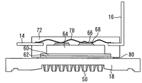
本実施形態は図1−9を参照して説明する。なお、異なる図番であっても同一の又は対応する構成要素には同一の符号を付して複数回の説明を省略する場合がある。他の実施形態でも同様である。
また、ピンフィン50を用いると後述のストレートフィンを用いた場合と比較して冷却器の剛性を下げることができる。よってはんだ80、はんだ90による接続の長期信頼性を高めることができる。
本実施形態は図10を参照して説明する。図10は実施形態1で説明した電力用半導体装置に主配線ブロックなどが付加された電力用半導体装置の外観を説明する図である。
本実施形態は図11を参照して説明する。図11は実施形態2で説明した電力用半導体装置に平滑コンデンサなどが付加された電力用半導体装置の外観を説明する図である。
本実施形態は図13−16を参照して説明する。図13は本実施形態の電力用半導体装置の外観を説明する図である。ただし説明の便宜上冷却器600については内部を記載する。第一冷却部602は冷媒通路となる空隙を形成するように第二冷却部604と固定される。そして、実施形態1のピンフィンに代えて、第一冷却部602にはストレートフィン606が配置される。同様に第二冷却部604にはストレートフィン608が配置される。
Claims (2)
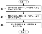
- モールド樹脂で封止され、前記モールド樹脂から露出する放熱面を有する第一パワーモジュールの前記放熱面と、第一冷却部の表面を第1はんだではんだ付けする第1工程と、
前記第一パワーモジュールと同じ構成の第二パワーモジュールの放熱面と、前記第一冷却部と同じ構成の第二冷却部の表面を第2はんだではんだ付けする第2工程と、
前記第1工程と前記第2工程の後に、前記第一冷却部と前記第二冷却部が冷媒通路となる空隙を形成するように、前記第一冷却部と前記第二冷却部を固着する第3工程とを備えたことを特徴とする電力用半導体装置の製造方法。 - 前記第3工程の前に、前記第1はんだにおけるボイドの有無を判定するX線検査を行う工程と、
前記第3工程の前に、前記第2はんだにおけるボイドの有無を判定するX線検査を行う工程と、を備えたことを特徴とする請求項1に記載の電力用半導体装置の製造方法。
Priority Applications (1)
| Application Number | Priority Date | Filing Date | Title |
|---|---|---|---|
| JP2013119038A JP5541393B2 (ja) | 2013-06-05 | 2013-06-05 | 電力用半導体装置の製造方法 |
Applications Claiming Priority (1)
| Application Number | Priority Date | Filing Date | Title |
|---|---|---|---|
| JP2013119038A JP5541393B2 (ja) | 2013-06-05 | 2013-06-05 | 電力用半導体装置の製造方法 |
Related Parent Applications (1)
| Application Number | Title | Priority Date | Filing Date |
|---|---|---|---|
| JP2009207447A Division JP5343775B2 (ja) | 2009-09-08 | 2009-09-08 | 電力用半導体装置 |
Publications (2)
| Publication Number | Publication Date |
|---|---|
| JP2013201454A JP2013201454A (ja) | 2013-10-03 |
| JP5541393B2 true JP5541393B2 (ja) | 2014-07-09 |
Family
ID=49521376
Family Applications (1)
| Application Number | Title | Priority Date | Filing Date |
|---|---|---|---|
| JP2013119038A Expired - Fee Related JP5541393B2 (ja) | 2013-06-05 | 2013-06-05 | 電力用半導体装置の製造方法 |
Country Status (1)
| Country | Link |
|---|---|
| JP (1) | JP5541393B2 (ja) |
Cited By (1)
| Publication number | Priority date | Publication date | Assignee | Title |
|---|---|---|---|---|
| US12016162B2 (en) | 2019-02-28 | 2024-06-18 | Audi Ag | Electric power converter device with improved integration of cooler frame |
Families Citing this family (1)
| Publication number | Priority date | Publication date | Assignee | Title |
|---|---|---|---|---|
| CN114361123B (zh) * | 2021-11-30 | 2025-08-05 | 江苏宏微科技股份有限公司 | 一种新型的多面散热功率半导体模块 |
Family Cites Families (4)
| Publication number | Priority date | Publication date | Assignee | Title |
|---|---|---|---|---|
| JPH10284685A (ja) * | 1997-04-04 | 1998-10-23 | Sansha Electric Mfg Co Ltd | 電力用半導体モジュール |
| JP2002270742A (ja) * | 2001-03-12 | 2002-09-20 | Unisia Jecs Corp | 半導体装置 |
| JP4213601B2 (ja) * | 2004-02-18 | 2009-01-21 | 株式会社デンソー | 半導体装置 |
| JP2006073893A (ja) * | 2004-09-03 | 2006-03-16 | Denso Corp | 半導体装置 |
-
2013
- 2013-06-05 JP JP2013119038A patent/JP5541393B2/ja not_active Expired - Fee Related
Cited By (1)
| Publication number | Priority date | Publication date | Assignee | Title |
|---|---|---|---|---|
| US12016162B2 (en) | 2019-02-28 | 2024-06-18 | Audi Ag | Electric power converter device with improved integration of cooler frame |
Also Published As
| Publication number | Publication date |
|---|---|
| JP2013201454A (ja) | 2013-10-03 |
Similar Documents
| Publication | Publication Date | Title |
|---|---|---|
| JP6384609B2 (ja) | パワー半導体モジュール及び冷却器 | |
| CN104285294B (zh) | 半导体装置及该半导体装置的制造方法 | |
| JP6315091B2 (ja) | 冷却器及び冷却器の固定方法 | |
| JP5306171B2 (ja) | 半導体装置 | |
| CN109698179B (zh) | 半导体装置及半导体装置的制造方法 | |
| JP6899784B2 (ja) | パワー半導体装置 | |
| WO2007145303A1 (ja) | 半導体モジュールおよびその製造方法 | |
| US20200144157A1 (en) | Semiconductor module and vehicle | |
| CN110771027B (zh) | 功率半导体装置及使用该装置的电力转换装置 | |
| CN107078659A (zh) | 电力转换装置 | |
| JP5343775B2 (ja) | 電力用半導体装置 | |
| WO2013088864A1 (ja) | 半導体装置 | |
| KR101930391B1 (ko) | 전자기기 | |
| JP4973059B2 (ja) | 半導体装置及び電力変換装置 | |
| JP4575034B2 (ja) | インバータ装置 | |
| WO2020184053A1 (ja) | 半導体装置 | |
| JP6286541B2 (ja) | パワーモジュール装置及び電力変換装置 | |
| JP5217015B2 (ja) | 電力変換装置及びその製造方法 | |
| JP5267238B2 (ja) | 半導体装置及び半導体装置の製造方法 | |
| JP5541393B2 (ja) | 電力用半導体装置の製造方法 | |
| JP2012138475A (ja) | 半導体モジュールおよび半導体モジュールの製造方法 | |
| CN114730748A (zh) | 用于消耗装置的可控电功率供应的具有被封装的功率半导体的功率模块及用于生产该功率模块的方法 | |
| CN105990275A (zh) | 功率模块封装件及其制作方法 | |
| JP5125530B2 (ja) | 電力変換装置 | |
| KR20180087330A (ko) | 파워 모듈의 양면 냉각을 위한 금속 슬러그 |
Legal Events
| Date | Code | Title | Description |
|---|---|---|---|
| A977 | Report on retrieval |
Free format text: JAPANESE INTERMEDIATE CODE: A971007 Effective date: 20140325 |
|
| TRDD | Decision of grant or rejection written | ||
| A01 | Written decision to grant a patent or to grant a registration (utility model) |
Free format text: JAPANESE INTERMEDIATE CODE: A01 Effective date: 20140408 |
|
| A61 | First payment of annual fees (during grant procedure) |
Free format text: JAPANESE INTERMEDIATE CODE: A61 Effective date: 20140421 |
|
| R150 | Certificate of patent or registration of utility model |
Ref document number: 5541393 Country of ref document: JP Free format text: JAPANESE INTERMEDIATE CODE: R150 |
|
| R250 | Receipt of annual fees |
Free format text: JAPANESE INTERMEDIATE CODE: R250 |
|
| R250 | Receipt of annual fees |
Free format text: JAPANESE INTERMEDIATE CODE: R250 |
|
| LAPS | Cancellation because of no payment of annual fees |