JP5579982B2 - 半導体装置の中間構造体及び中間構造体の製造方法 - Google Patents
半導体装置の中間構造体及び中間構造体の製造方法 Download PDFInfo
- Publication number
- JP5579982B2 JP5579982B2 JP2008318699A JP2008318699A JP5579982B2 JP 5579982 B2 JP5579982 B2 JP 5579982B2 JP 2008318699 A JP2008318699 A JP 2008318699A JP 2008318699 A JP2008318699 A JP 2008318699A JP 5579982 B2 JP5579982 B2 JP 5579982B2
- Authority
- JP
- Japan
- Prior art keywords
- resin
- wiring board
- thickness
- intermediate structure
- sealing body
- Prior art date
- Legal status (The legal status is an assumption and is not a legal conclusion. Google has not performed a legal analysis and makes no representation as to the accuracy of the status listed.)
- Expired - Fee Related
Links
Images








Classifications
-
- H—ELECTRICITY
- H10—SEMICONDUCTOR DEVICES; ELECTRIC SOLID-STATE DEVICES NOT OTHERWISE PROVIDED FOR
- H10W—GENERIC PACKAGES, INTERCONNECTIONS, CONNECTORS OR OTHER CONSTRUCTIONAL DETAILS OF DEVICES COVERED BY CLASS H10
- H10W74/00—Encapsulations, e.g. protective coatings
- H10W74/10—Encapsulations, e.g. protective coatings characterised by their shape or disposition
- H10W74/111—Encapsulations, e.g. protective coatings characterised by their shape or disposition the semiconductor body being completely enclosed
- H10W74/114—Encapsulations, e.g. protective coatings characterised by their shape or disposition the semiconductor body being completely enclosed by a substrate and the encapsulations
- H10W74/117—Encapsulations, e.g. protective coatings characterised by their shape or disposition the semiconductor body being completely enclosed by a substrate and the encapsulations the substrate having spherical bumps for external connection
-
- H—ELECTRICITY
- H10—SEMICONDUCTOR DEVICES; ELECTRIC SOLID-STATE DEVICES NOT OTHERWISE PROVIDED FOR
- H10W—GENERIC PACKAGES, INTERCONNECTIONS, CONNECTORS OR OTHER CONSTRUCTIONAL DETAILS OF DEVICES COVERED BY CLASS H10
- H10W74/00—Encapsulations, e.g. protective coatings
- H10W74/01—Manufacture or treatment
- H10W74/014—Manufacture or treatment using batch processing
-
- H—ELECTRICITY
- H10—SEMICONDUCTOR DEVICES; ELECTRIC SOLID-STATE DEVICES NOT OTHERWISE PROVIDED FOR
- H10W—GENERIC PACKAGES, INTERCONNECTIONS, CONNECTORS OR OTHER CONSTRUCTIONAL DETAILS OF DEVICES COVERED BY CLASS H10
- H10W74/00—Encapsulations, e.g. protective coatings
- H10W74/01—Manufacture or treatment
- H10W74/016—Manufacture or treatment using moulds
-
- H—ELECTRICITY
- H10—SEMICONDUCTOR DEVICES; ELECTRIC SOLID-STATE DEVICES NOT OTHERWISE PROVIDED FOR
- H10W—GENERIC PACKAGES, INTERCONNECTIONS, CONNECTORS OR OTHER CONSTRUCTIONAL DETAILS OF DEVICES COVERED BY CLASS H10
- H10W72/00—Interconnections or connectors in packages
- H10W72/01—Manufacture or treatment
- H10W72/0198—Manufacture or treatment batch processes
-
- H—ELECTRICITY
- H10—SEMICONDUCTOR DEVICES; ELECTRIC SOLID-STATE DEVICES NOT OTHERWISE PROVIDED FOR
- H10W—GENERIC PACKAGES, INTERCONNECTIONS, CONNECTORS OR OTHER CONSTRUCTIONAL DETAILS OF DEVICES COVERED BY CLASS H10
- H10W72/00—Interconnections or connectors in packages
- H10W72/50—Bond wires
- H10W72/541—Dispositions of bond wires
- H10W72/5449—Dispositions of bond wires not being orthogonal to a side surface of the chip, e.g. fan-out arrangements
-
- H—ELECTRICITY
- H10—SEMICONDUCTOR DEVICES; ELECTRIC SOLID-STATE DEVICES NOT OTHERWISE PROVIDED FOR
- H10W—GENERIC PACKAGES, INTERCONNECTIONS, CONNECTORS OR OTHER CONSTRUCTIONAL DETAILS OF DEVICES COVERED BY CLASS H10
- H10W72/00—Interconnections or connectors in packages
- H10W72/50—Bond wires
- H10W72/551—Materials of bond wires
- H10W72/552—Materials of bond wires comprising metals or metalloids, e.g. silver
- H10W72/5522—Materials of bond wires comprising metals or metalloids, e.g. silver comprising gold [Au]
-
- H—ELECTRICITY
- H10—SEMICONDUCTOR DEVICES; ELECTRIC SOLID-STATE DEVICES NOT OTHERWISE PROVIDED FOR
- H10W—GENERIC PACKAGES, INTERCONNECTIONS, CONNECTORS OR OTHER CONSTRUCTIONAL DETAILS OF DEVICES COVERED BY CLASS H10
- H10W72/00—Interconnections or connectors in packages
- H10W72/50—Bond wires
- H10W72/551—Materials of bond wires
- H10W72/552—Materials of bond wires comprising metals or metalloids, e.g. silver
- H10W72/5525—Materials of bond wires comprising metals or metalloids, e.g. silver comprising copper [Cu]
-
- H—ELECTRICITY
- H10—SEMICONDUCTOR DEVICES; ELECTRIC SOLID-STATE DEVICES NOT OTHERWISE PROVIDED FOR
- H10W—GENERIC PACKAGES, INTERCONNECTIONS, CONNECTORS OR OTHER CONSTRUCTIONAL DETAILS OF DEVICES COVERED BY CLASS H10
- H10W72/00—Interconnections or connectors in packages
- H10W72/851—Dispositions of multiple connectors or interconnections
- H10W72/874—On different surfaces
- H10W72/884—Die-attach connectors and bond wires
-
- H—ELECTRICITY
- H10—SEMICONDUCTOR DEVICES; ELECTRIC SOLID-STATE DEVICES NOT OTHERWISE PROVIDED FOR
- H10W—GENERIC PACKAGES, INTERCONNECTIONS, CONNECTORS OR OTHER CONSTRUCTIONAL DETAILS OF DEVICES COVERED BY CLASS H10
- H10W74/00—Encapsulations, e.g. protective coatings
-
- H—ELECTRICITY
- H10—SEMICONDUCTOR DEVICES; ELECTRIC SOLID-STATE DEVICES NOT OTHERWISE PROVIDED FOR
- H10W—GENERIC PACKAGES, INTERCONNECTIONS, CONNECTORS OR OTHER CONSTRUCTIONAL DETAILS OF DEVICES COVERED BY CLASS H10
- H10W90/00—Package configurations
- H10W90/701—Package configurations characterised by the relative positions of pads or connectors relative to package parts
- H10W90/731—Package configurations characterised by the relative positions of pads or connectors relative to package parts of die-attach connectors
- H10W90/734—Package configurations characterised by the relative positions of pads or connectors relative to package parts of die-attach connectors between a chip and a stacked insulating package substrate, interposer or RDL
-
- H—ELECTRICITY
- H10—SEMICONDUCTOR DEVICES; ELECTRIC SOLID-STATE DEVICES NOT OTHERWISE PROVIDED FOR
- H10W—GENERIC PACKAGES, INTERCONNECTIONS, CONNECTORS OR OTHER CONSTRUCTIONAL DETAILS OF DEVICES COVERED BY CLASS H10
- H10W90/00—Package configurations
- H10W90/701—Package configurations characterised by the relative positions of pads or connectors relative to package parts
- H10W90/751—Package configurations characterised by the relative positions of pads or connectors relative to package parts of bond wires
- H10W90/754—Package configurations characterised by the relative positions of pads or connectors relative to package parts of bond wires between a chip and a stacked insulating package substrate, interposer or RDL
Landscapes
- Encapsulation Of And Coatings For Semiconductor Or Solid State Devices (AREA)
Description
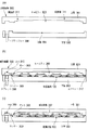
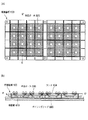
図1〜図7を参照して、本発明の第1の実施形態に係るBGA(Ball Grid Array)型半導体装置の製造方法について説明する。
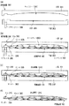
図8は、本発明の第2の実施の形態に係るBGA型半導体装置の封止工程を示す断面図、図9は第2の実施の形態の封止工程により形成した中間構造体の概略構成を示す平面図及び断面図である。以下、図8及び図9を参照して、第2の実施の形態に係る半導体装置の封止工程について説明する。
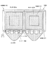
図10は、第3の実施の形態に係るBGA型半導体装置の封止工程を示す断面図、図11は第3の実施の形態の封止工程により形成した中間構造体の概略構成を示す平面図及び断面図である。図10及び図11を参照して、第3の実施の形態に係る半導体装置の封止工程について説明する。
図12は、第4の実施の形態の封止工程により形成した中間構造体の概略構成を示す平面図である。
101 製品形成部
102a,102b エリア
103 接続パッド
104 ランド
105 配線
106 枠部
107 位置決め孔
108 ダイシングライン
109 半導体チップ
110 ワイヤ
300 成型装置
301 上型
302 下型
303 キャビティ
304 凹部
305 ゲート
306 タブレット
307 封止樹脂
308 プランジャー
309 ランナー
310 カル
311 段差部
400 中間構造体
Claims (16)
- 配線基板と、
配線基板に搭載された複数の半導体チップと、
複数の半導体チップを一括的に封止し、かつ厚さの異なる部位を有する封止体を有し、
前記封止体は、ゲート側の厚さがエアベント側の厚さより薄くなるように形成されていることを特徴とする半導体装置の中間構造体。 - 前記厚さの異なる部位は、前記配線基板及び前記半導体装置の少なくとも一つの反りを低減するために形成されていることを特徴とする請求項1に記載の中間構造体。
- 前記封止体は、前記ゲート側から前記エアベント側に向かって、段階的に又は連続的に厚さが大きくなるように形成されていることを特徴とする請求項1に記載の中間構造体。
- 前記配線基板は、製品形成エリアと製品形成エリアの外側に設けられた周辺部とを有し、
前記封止体は、前記周辺部の厚さが前記製品形成エリアの厚さより薄くなるように形成されていることを特徴とする請求項1に記載の中間構造体。 - 前記製品形成エリアには、それぞれ一つの前記半導体チップが配置された複数の製品形成部が設けられており、
前記周辺部は、前記配線基板の枠部に設けられていることを特徴とする請求項4に記載の中間構造体。 - 複数の製品形成部を有する配線基板を用意し、
各製品形成部に半導体チップを搭載し、
深さが異なるキャビティを有する成型装置を使用して、キャビティ内に樹脂を注入して複数の半導体チップを一括的に封止し、これにより樹脂厚の異なる部位を有する封止体を形成し、
前記キャビティは、ゲート側の深さがエアベント側の深さより浅く形成されており、
前記キャビティ内に前記樹脂を注入することにより、前記封止体を、前記ゲート側の樹脂厚が前記エアベント側の樹脂厚より薄くなるように形成することを特徴とする半導体装置の中間構造体の製造方法。 - 前記樹脂厚の異なる部位は、前記配線基板及び前記半導体装置の少なくとも一つの反りを低減するために形成されていることを特徴とする請求項6に記載の中間構造体の製造方法。
- 前記キャビティは、前記ゲート側の深さが前記エアベント側の深さより段階的又は連続的に浅く形成されており、
前記封止体は、前記ゲート側から前記エアベント側に向かって、段階的に又は連続的に樹脂厚が大きくなるように形成されていることを特徴とする請求項6に記載の中間構造体の製造方法。 - 前記製品形成部の外側には周辺部が形成されており、
前記キャビティは、前記周辺部の深さが前記製品形成部の深さより浅く形成されており、
前記キャビティ内に前記樹脂を注入することにより、前記封止体を、前記周辺部の樹脂厚が前記製品形成部の樹脂厚より薄くなるように形成することを特徴とする請求項6又は7に記載の中間構造体の製造方法。 - 前記封止体は、前記キャビティの両端部の近傍部位を含めて略等間隔で配置された複数のゲートから前記樹脂を注入することにより形成されることを特徴とする請求項6及至9のいずれか1項に記載の中間構造体の製造方法。
- 請求項6及至10のいずれか1項に記載の製造方法により得られた前記中間構造体をダイシングすることにより、複数の半導体装置を得ることを特徴とする半導体装置の製造方法。
- 請求項6及至10のいずれか1項に記載の製造方法で使用された深さが異なる前記キャビティを有する成型装置。
- 配線基板と、
配線基板に搭載された複数の半導体チップと、
複数の半導体チップを一括的に封止し、かつ厚さの異なる部位を有する封止体を有し、
前記封止体は、略長方形状に構成されており、短辺側の周辺部位の厚さが長辺側の周辺部位の厚さより薄く形成されていることを特徴とする半導体装置の中間構造体。 - 配線基板と、
配線基板に搭載された複数の半導体チップと、
複数の半導体チップを一括的に封止し、かつ厚さの異なる部位を有する封止体を有し、
前記封止体は、略長方形状に構成されており、短辺側の周辺部位の厚さの薄い領域が、長辺側の厚さの薄い領域より広く形成されていることを特徴とする半導体装置の中間構造体。 - 複数の製品形成部を有する配線基板を用意し、
各製品形成部に半導体チップを搭載し、
深さが異なるキャビティを有する成型装置を使用して、キャビティ内に樹脂を注入して複数の半導体チップを一括的に封止し、これにより樹脂厚の異なる部位を有する封止体を形成し、
前記封止体は略長方形状に形成され、短辺側の周辺部位の樹脂厚が長辺側の周辺部位の樹脂厚より薄く形成されていることを特徴とする半導体装置の中間構造体の製造方法。 - 複数の製品形成部を有する配線基板を用意し、
各製品形成部に半導体チップを搭載し、
深さが異なるキャビティを有する成型装置を使用して、キャビティ内に樹脂を注入して複数の半導体チップを一括的に封止し、これにより樹脂厚の異なる部位を有する封止体を形成し、
前記封止体は、略長方形状に形成され、短辺側の周辺部位の樹脂厚の薄い領域が、長辺側の樹脂厚の薄い領域より広く形成されていることを特徴とする半導体装置の中間構造体の製造方法。
Priority Applications (2)
| Application Number | Priority Date | Filing Date | Title |
|---|---|---|---|
| JP2008318699A JP5579982B2 (ja) | 2008-12-15 | 2008-12-15 | 半導体装置の中間構造体及び中間構造体の製造方法 |
| US12/636,959 US8198141B2 (en) | 2008-12-15 | 2009-12-14 | Intermediate structure of semiconductor device and method of manufacturing the same |
Applications Claiming Priority (1)
| Application Number | Priority Date | Filing Date | Title |
|---|---|---|---|
| JP2008318699A JP5579982B2 (ja) | 2008-12-15 | 2008-12-15 | 半導体装置の中間構造体及び中間構造体の製造方法 |
Publications (2)
| Publication Number | Publication Date |
|---|---|
| JP2010141261A JP2010141261A (ja) | 2010-06-24 |
| JP5579982B2 true JP5579982B2 (ja) | 2014-08-27 |
Family
ID=42239543
Family Applications (1)
| Application Number | Title | Priority Date | Filing Date |
|---|---|---|---|
| JP2008318699A Expired - Fee Related JP5579982B2 (ja) | 2008-12-15 | 2008-12-15 | 半導体装置の中間構造体及び中間構造体の製造方法 |
Country Status (2)
| Country | Link |
|---|---|
| US (1) | US8198141B2 (ja) |
| JP (1) | JP5579982B2 (ja) |
Cited By (1)
| Publication number | Priority date | Publication date | Assignee | Title |
|---|---|---|---|---|
| US11069588B2 (en) | 2018-08-01 | 2021-07-20 | Samsung Electronics Co., Ltd. | Semiconductor package and method of manufacturing the same |
Families Citing this family (3)
| Publication number | Priority date | Publication date | Assignee | Title |
|---|---|---|---|---|
| JP5512292B2 (ja) * | 2010-01-08 | 2014-06-04 | ルネサスエレクトロニクス株式会社 | 半導体装置の製造方法 |
| US8753926B2 (en) * | 2010-09-14 | 2014-06-17 | Qualcomm Incorporated | Electronic packaging with a variable thickness mold cap |
| JP2017183511A (ja) | 2016-03-30 | 2017-10-05 | ルネサスエレクトロニクス株式会社 | 半導体装置の製造方法 |
Family Cites Families (26)
| Publication number | Priority date | Publication date | Assignee | Title |
|---|---|---|---|---|
| US5108955A (en) * | 1988-10-27 | 1992-04-28 | Citizen Watch Co., Ltd. | Method of making a resin encapsulated pin grid array with integral heatsink |
| JP2725637B2 (ja) * | 1995-05-31 | 1998-03-11 | 日本電気株式会社 | 電子回路装置およびその製造方法 |
| US5744084A (en) * | 1995-07-24 | 1998-04-28 | Lsi Logic Corporation | Method of improving molding of an overmolded package body on a substrate |
| US5612513A (en) * | 1995-09-19 | 1997-03-18 | Micron Communications, Inc. | Article and method of manufacturing an enclosed electrical circuit using an encapsulant |
| JPH10326800A (ja) | 1997-05-26 | 1998-12-08 | Seiko Epson Corp | 半導体装置の製造方法及び半導体製造装置用金型 |
| JP3521325B2 (ja) * | 1999-07-30 | 2004-04-19 | シャープ株式会社 | 樹脂封止型半導体装置の製造方法 |
| JP3544895B2 (ja) * | 1999-07-30 | 2004-07-21 | シャープ株式会社 | 樹脂封止型半導体装置及びその製造方法 |
| JP3214619B2 (ja) * | 1999-11-26 | 2001-10-02 | アルス精密株式会社 | 半導体パッケージの製造方法 |
| US6963141B2 (en) * | 1999-12-31 | 2005-11-08 | Jung-Yu Lee | Semiconductor package for efficient heat spreading |
| JP2001210755A (ja) * | 2000-01-28 | 2001-08-03 | Nec Corp | 半導体装置用基板および半導体装置の製造方法 |
| JP2001257291A (ja) * | 2000-03-13 | 2001-09-21 | Sanyo Electric Co Ltd | 回路装置 |
| JP2002009097A (ja) * | 2000-06-22 | 2002-01-11 | Oki Electric Ind Co Ltd | 半導体装置とその製造方法 |
| US6546620B1 (en) * | 2000-06-29 | 2003-04-15 | Amkor Technology, Inc. | Flip chip integrated circuit and passive chip component package fabrication method |
| JP3453113B2 (ja) * | 2000-08-09 | 2003-10-06 | サンユレック株式会社 | 電子部品の製造方法及び当該方法で用いる液状樹脂 |
| US6709170B2 (en) * | 2001-01-08 | 2004-03-23 | Optical Communications Products, Inc. | Plastic encapsulation of optoelectronic devices for optical coupling |
| JP3881189B2 (ja) * | 2001-04-23 | 2007-02-14 | 株式会社ルネサステクノロジ | 半導体装置の製造方法 |
| CA2350747C (en) * | 2001-06-15 | 2005-08-16 | Ibm Canada Limited-Ibm Canada Limitee | Improved transfer molding of integrated circuit packages |
| US7001083B1 (en) * | 2001-09-21 | 2006-02-21 | National Semiconductor Corporation | Technique for protecting photonic devices in optoelectronic packages with clear overmolding |
| JP3708871B2 (ja) * | 2001-12-20 | 2005-10-19 | 株式会社シチズン電子 | 半導体パッケージ集合物 |
| US6838759B1 (en) * | 2003-11-10 | 2005-01-04 | Kingpak Technology Inc. | Small memory card |
| JP2005150350A (ja) * | 2003-11-14 | 2005-06-09 | Renesas Technology Corp | 半導体装置の製造方法 |
| JP2005333044A (ja) * | 2004-05-21 | 2005-12-02 | Matsushita Electric Ind Co Ltd | 半導体装置の製造方法 |
| KR100761387B1 (ko) * | 2005-07-13 | 2007-09-27 | 서울반도체 주식회사 | 몰딩부재를 형성하기 위한 몰드 및 그것을 사용한 몰딩부재형성방법 |
| US7808004B2 (en) * | 2006-03-17 | 2010-10-05 | Edison Opto Corporation | Light emitting diode package structure and method of manufacturing the same |
| JP4935163B2 (ja) | 2006-04-11 | 2012-05-23 | 日本電気株式会社 | 半導体チップ搭載用基板 |
| TW200945545A (en) * | 2007-12-12 | 2009-11-01 | United Test & Assembly Ct Lt | Package-on-package semiconductor structure |
-
2008
- 2008-12-15 JP JP2008318699A patent/JP5579982B2/ja not_active Expired - Fee Related
-
2009
- 2009-12-14 US US12/636,959 patent/US8198141B2/en not_active Expired - Fee Related
Cited By (2)
| Publication number | Priority date | Publication date | Assignee | Title |
|---|---|---|---|---|
| US11069588B2 (en) | 2018-08-01 | 2021-07-20 | Samsung Electronics Co., Ltd. | Semiconductor package and method of manufacturing the same |
| US11699626B2 (en) | 2018-08-01 | 2023-07-11 | Samsung Electronics Co., Ltd. | Semiconductor package and method of manufacturing the same |
Also Published As
| Publication number | Publication date |
|---|---|
| US8198141B2 (en) | 2012-06-12 |
| US20100148377A1 (en) | 2010-06-17 |
| JP2010141261A (ja) | 2010-06-24 |
Similar Documents
| Publication | Publication Date | Title |
|---|---|---|
| US8546183B2 (en) | Method for fabricating heat dissipating semiconductor package | |
| US6767767B2 (en) | Method of manufacturing a semiconductor device in which a block molding package utilizes air vents in a substrate | |
| US7911047B2 (en) | Semiconductor device and method of fabricating the semiconductor device | |
| US20080160678A1 (en) | Method for fabricating semiconductor package | |
| JP5543058B2 (ja) | 半導体装置の製造方法 | |
| JP2010153466A (ja) | 配線基板 | |
| JP2002110718A (ja) | 半導体装置の製造方法 | |
| US9659842B2 (en) | Methods of fabricating QFN semiconductor package and metal plate | |
| US20140091479A1 (en) | Semiconductor device with stacked semiconductor chips | |
| JP5557439B2 (ja) | 半導体装置及びその製造方法 | |
| JP5579982B2 (ja) | 半導体装置の中間構造体及び中間構造体の製造方法 | |
| US9117741B2 (en) | Semiconductor device | |
| US20050258552A1 (en) | Semiconductor molding method and structure | |
| JP4497304B2 (ja) | 半導体装置及びその製造方法 | |
| JP2010272734A (ja) | 半導体装置及びその製造方法 | |
| JP2016025198A (ja) | 半導体装置の製造方法 | |
| JP2011061055A (ja) | 半導体装置の製造方法 | |
| JP5666211B2 (ja) | 配線基板及び半導体装置の製造方法 | |
| JP2011151104A (ja) | 半導体装置の製造方法及び半導体装置の中間構造体 | |
| TWI420626B (zh) | 封裝結構與封裝製程 | |
| JP2012169398A (ja) | 半導体装置の製造方法 | |
| US20060284340A1 (en) | Method for preventing the overflowing of molding compound during fabricating package device | |
| KR20050063052A (ko) | 멀티칩 패키지 구조 및 그 제조방법 | |
| JP2004158539A (ja) | 樹脂封止型半導体装置の製造方法 | |
| JP2016062985A (ja) | 半導体装置の製造方法 |
Legal Events
| Date | Code | Title | Description |
|---|---|---|---|
| A621 | Written request for application examination |
Free format text: JAPANESE INTERMEDIATE CODE: A621 Effective date: 20111003 |
|
| A711 | Notification of change in applicant |
Free format text: JAPANESE INTERMEDIATE CODE: A711 Effective date: 20130730 |
|
| A131 | Notification of reasons for refusal |
Free format text: JAPANESE INTERMEDIATE CODE: A131 Effective date: 20131030 |
|
| A601 | Written request for extension of time |
Free format text: JAPANESE INTERMEDIATE CODE: A601 Effective date: 20140114 |
|
| A602 | Written permission of extension of time |
Free format text: JAPANESE INTERMEDIATE CODE: A602 Effective date: 20140117 |
|
| A521 | Request for written amendment filed |
Free format text: JAPANESE INTERMEDIATE CODE: A523 Effective date: 20140424 |
|
| TRDD | Decision of grant or rejection written | ||
| A01 | Written decision to grant a patent or to grant a registration (utility model) |
Free format text: JAPANESE INTERMEDIATE CODE: A01 Effective date: 20140618 |
|
| A61 | First payment of annual fees (during grant procedure) |
Free format text: JAPANESE INTERMEDIATE CODE: A61 Effective date: 20140710 |
|
| R150 | Certificate of patent or registration of utility model |
Ref document number: 5579982 Country of ref document: JP Free format text: JAPANESE INTERMEDIATE CODE: R150 |
|
| LAPS | Cancellation because of no payment of annual fees |