JP5580247B2 - パターン検査装置 - Google Patents
パターン検査装置 Download PDFInfo
- Publication number
- JP5580247B2 JP5580247B2 JP2011099735A JP2011099735A JP5580247B2 JP 5580247 B2 JP5580247 B2 JP 5580247B2 JP 2011099735 A JP2011099735 A JP 2011099735A JP 2011099735 A JP2011099735 A JP 2011099735A JP 5580247 B2 JP5580247 B2 JP 5580247B2
- Authority
- JP
- Japan
- Prior art keywords
- line
- shaped electrode
- disconnection
- timing
- inspection apparatus
- Prior art date
- Legal status (The legal status is an assumption and is not a legal conclusion. Google has not performed a legal analysis and makes no representation as to the accuracy of the status listed.)
- Active
Links
Images




Classifications
-
- G—PHYSICS
- G01—MEASURING; TESTING
- G01R—MEASURING ELECTRIC VARIABLES; MEASURING MAGNETIC VARIABLES
- G01R31/00—Arrangements for testing electric properties; Arrangements for locating electric faults; Arrangements for electrical testing characterised by what is being tested not provided for elsewhere
- G01R31/28—Testing of electronic circuits, e.g. by signal tracer
- G01R31/2832—Specific tests of electronic circuits not provided for elsewhere
- G01R31/2836—Fault-finding or characterising
- G01R31/2837—Characterising or performance testing, e.g. of frequency response
-
- G—PHYSICS
- G01—MEASURING; TESTING
- G01R—MEASURING ELECTRIC VARIABLES; MEASURING MAGNETIC VARIABLES
- G01R31/00—Arrangements for testing electric properties; Arrangements for locating electric faults; Arrangements for electrical testing characterised by what is being tested not provided for elsewhere
- G01R31/28—Testing of electronic circuits, e.g. by signal tracer
- G01R31/2851—Testing of integrated circuits [IC]
- G01R31/2855—Environmental, reliability or burn-in testing
- G01R31/2872—Environmental, reliability or burn-in testing related to electrical or environmental aspects, e.g. temperature, humidity, vibration, nuclear radiation
- G01R31/2879—Environmental, reliability or burn-in testing related to electrical or environmental aspects, e.g. temperature, humidity, vibration, nuclear radiation related to electrical aspects, e.g. to voltage or current supply or stimuli or to electrical loads
-
- G—PHYSICS
- G01—MEASURING; TESTING
- G01R—MEASURING ELECTRIC VARIABLES; MEASURING MAGNETIC VARIABLES
- G01R31/00—Arrangements for testing electric properties; Arrangements for locating electric faults; Arrangements for electrical testing characterised by what is being tested not provided for elsewhere
- G01R31/28—Testing of electronic circuits, e.g. by signal tracer
- G01R31/2851—Testing of integrated circuits [IC]
- G01R31/2884—Testing of integrated circuits [IC] using dedicated test connectors, test elements or test circuits on the IC under test
Landscapes
- Engineering & Computer Science (AREA)
- General Engineering & Computer Science (AREA)
- Physics & Mathematics (AREA)
- General Physics & Mathematics (AREA)
- Environmental & Geological Engineering (AREA)
- Computer Hardware Design (AREA)
- Microelectronics & Electronic Packaging (AREA)
- Health & Medical Sciences (AREA)
- Toxicology (AREA)
- Testing Of Short-Circuits, Discontinuities, Leakage, Or Incorrect Line Connections (AREA)
- Measurement Of Length, Angles, Or The Like Using Electric Or Magnetic Means (AREA)
- Liquid Crystal (AREA)
Description
Claims (5)
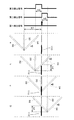
- 基板上において第一方向に間隔をあけて配設された複数の導電パターンのうち、断線が生じた導電パターンにおいて断線位置を検出するパターン検査装置であって、
前記断線が生じた導電パターンの一端から交流電圧を印加する印加手段と、
前記基板に間隙を介して対向しつつ、前記複数の導電パターンを横断する方向に移動するセンサと、
前記センサに設けられ、互いに異なる方向に延びるとともに互いに電気的に絶縁された2以上のライン状電極であって、それぞれが対向する導電パターンと静電結合する2以上のライン状電極と、
前記2以上のライン状電極それぞれで検知される電圧信号の変動タイミングに基づいて、前記断線位置を特定する制御部と、
を備えることを特徴とするパターン検査装置。 - 請求項1に記載のパターン検査装置であって、
前記2以上のライン状電極は、少なくとも、第一方向と直交する第二方向に延びる第一ライン状電極と、第一ライン状電極に対して傾斜した方向に延びる第二ライン状電極と、を備え、
前記制御部は、
前記第一ライン状電極で検知された電圧信号の急変タイミングに基づいて、前記断線の第一方向の位置を特定し、
前記第一ライン状電極で検知された電圧信号の急変タイミングおよび前記第二ライン状電極で検知された電圧信号の急変タイミングに基づいて、前記断線の第二方向の位置を特定する、
ことを特徴とするパターン検査装置。 - 請求項2に記載のパターン検査装置であって、
前記2以上のライン状電極は、さらに、第一ライン状電極に対して傾斜し、第二ライン状電極とは逆の極性に傾斜した方向に延びる第三ライン状電極を備え、
前記制御部は、
前記第一ライン状電極で検知された電圧信号の急変タイミング、および、前記第二ライン状電極または第三ライン状電極で検知された電圧信号の急変タイミングに基づいて、前記断線の第二方向の位置を特定する、
ことを特徴とするパターン検査装置。 - 請求項3に記載のパターン検査装置であって、
第一ライン状電極に対して、前記第二ライン状電極は45度、第三ライン状電極は−45度、それぞれ傾斜している、ことを特徴とするパターン検査装置。 - 請求項1から4のいずれか1項に記載のパターン検査装置であって、
前記基板には、
複数の導電パターンが第一の間隔をあけて第一方向に配設される画素領域と、
前記画素領域の外側に設けられ、導電パターン間の間隔が徐々に変化するように前記複数の導電パターンが配設された領域を有する外部領域と、
が形成されており、
各ライン状電極は、少なくとも、前記外部領域を縦断する長さを有しており、
前記制御部は、ライン状電極それぞれで検知される電圧信号の変動タイミングに基づいて、前記外部領域での断線位置を特定する、
ことを特徴とするパターン検査装置。
Priority Applications (4)
| Application Number | Priority Date | Filing Date | Title |
|---|---|---|---|
| JP2011099735A JP5580247B2 (ja) | 2011-04-27 | 2011-04-27 | パターン検査装置 |
| TW100142768A TWI418814B (zh) | 2011-04-27 | 2011-11-22 | 導電圖案檢查裝置 |
| CN201210026184.XA CN102759679B (zh) | 2011-04-27 | 2012-02-07 | 导电图案检查装置 |
| KR1020120014791A KR101264764B1 (ko) | 2011-04-27 | 2012-02-14 | 도전 패턴 검사 장치 |
Applications Claiming Priority (1)
| Application Number | Priority Date | Filing Date | Title |
|---|---|---|---|
| JP2011099735A JP5580247B2 (ja) | 2011-04-27 | 2011-04-27 | パターン検査装置 |
Publications (2)
| Publication Number | Publication Date |
|---|---|
| JP2012230062A JP2012230062A (ja) | 2012-11-22 |
| JP5580247B2 true JP5580247B2 (ja) | 2014-08-27 |
Family
ID=47054191
Family Applications (1)
| Application Number | Title | Priority Date | Filing Date |
|---|---|---|---|
| JP2011099735A Active JP5580247B2 (ja) | 2011-04-27 | 2011-04-27 | パターン検査装置 |
Country Status (4)
| Country | Link |
|---|---|
| JP (1) | JP5580247B2 (ja) |
| KR (1) | KR101264764B1 (ja) |
| CN (1) | CN102759679B (ja) |
| TW (1) | TWI418814B (ja) |
Families Citing this family (1)
| Publication number | Priority date | Publication date | Assignee | Title |
|---|---|---|---|---|
| EP4528259A4 (en) * | 2022-05-18 | 2026-04-22 | Leadway Hk Ltd | BIOSENSOR AND CORRESPONDING MANUFACTURING PROCESS |
Family Cites Families (14)
| Publication number | Priority date | Publication date | Assignee | Title |
|---|---|---|---|---|
| JP3589923B2 (ja) * | 1999-01-21 | 2004-11-17 | シャープ株式会社 | 電極パターン検査装置および電極パターン検査方法 |
| JP2002365325A (ja) * | 2001-06-11 | 2002-12-18 | Oht Inc | 回路パターン検査装置並びに回路パターン検査方法及び記録媒体 |
| CN1720458B (zh) * | 2002-11-30 | 2010-06-23 | Oht株式会社 | 电路图案检查装置及电路图案检查方法 |
| JP4562358B2 (ja) * | 2003-07-04 | 2010-10-13 | 株式会社ユニオンアロー・テクノロジー | 導電パターン検査装置 |
| JP4559204B2 (ja) * | 2004-12-10 | 2010-10-06 | 日置電機株式会社 | 回路基板検査装置および回路基板検査方法 |
| JP4417858B2 (ja) * | 2005-01-19 | 2010-02-17 | オー・エイチ・ティー株式会社 | 回路パターン検査装置およびその方法 |
| JP3989488B2 (ja) * | 2005-01-19 | 2007-10-10 | オー・エイチ・ティー株式会社 | 検査装置及び検査方法並びに検査装置用センサ |
| JP2006200993A (ja) * | 2005-01-19 | 2006-08-03 | Oht Inc | 回路パターン検査装置およびその方法 |
| JP2006300665A (ja) * | 2005-04-19 | 2006-11-02 | Oht Inc | 検査装置および導電パターン検査方法 |
| JP4291843B2 (ja) * | 2006-10-19 | 2009-07-08 | 株式会社東京カソード研究所 | パターン検査装置 |
| JP4856120B2 (ja) * | 2008-06-06 | 2012-01-18 | 株式会社ユニオンアロー・テクノロジー | 導電パターン検査装置 |
| JP5290697B2 (ja) * | 2008-10-20 | 2013-09-18 | 日置電機株式会社 | 基準データ作成方法および回路基板検査装置 |
| CN201387525Y (zh) * | 2009-03-04 | 2010-01-20 | 深圳市宇顺电子股份有限公司 | 一种液晶显示器基板测试装置 |
| JP4644745B2 (ja) * | 2009-08-04 | 2011-03-02 | オー・エイチ・ティー株式会社 | 回路パターン検査装置 |
-
2011
- 2011-04-27 JP JP2011099735A patent/JP5580247B2/ja active Active
- 2011-11-22 TW TW100142768A patent/TWI418814B/zh not_active IP Right Cessation
-
2012
- 2012-02-07 CN CN201210026184.XA patent/CN102759679B/zh not_active Expired - Fee Related
- 2012-02-14 KR KR1020120014791A patent/KR101264764B1/ko not_active Expired - Fee Related
Also Published As
| Publication number | Publication date |
|---|---|
| TW201243354A (en) | 2012-11-01 |
| CN102759679A (zh) | 2012-10-31 |
| KR101264764B1 (ko) | 2013-05-15 |
| JP2012230062A (ja) | 2012-11-22 |
| TWI418814B (zh) | 2013-12-11 |
| CN102759679B (zh) | 2014-08-06 |
| KR20120121824A (ko) | 2012-11-06 |
Similar Documents
| Publication | Publication Date | Title |
|---|---|---|
| JP5131962B2 (ja) | 非接触シングルサイドプローブ及び、これを用いたパターン電極の断線・短絡検査装置及びその方法 | |
| KR20110005649A (ko) | 터치장치에 사용되는 터치위치의 측정방법 | |
| JP5387818B2 (ja) | 回路パターン検査装置 | |
| US10802063B2 (en) | Detection device and detection method | |
| KR20100028275A (ko) | 평판 디스플레이의 전극라인 검사 장치 및 방법 | |
| JP6248406B2 (ja) | 検査装置及び検査方法 | |
| KR20110066291A (ko) | 회로기판의 검사장치 | |
| JP5580247B2 (ja) | パターン検査装置 | |
| US20150338976A1 (en) | Touch display device | |
| TWI474012B (zh) | 導電圖案檢查裝置及檢查方法 | |
| WO2004057350A1 (ja) | 回路パターン検査装置及びパターン検査方法 | |
| JP5432213B2 (ja) | パターン検査装置 | |
| KR20080098088A (ko) | 비접촉 싱글사이드 프로브와 이를 이용한 패턴전극의 단선및 단락 검사장치 및 그 방법 | |
| TW200537112A (en) | Circuit pattern testing apparatus and circuit pattern testing method | |
| JP5607335B2 (ja) | 静電容量式近接センサ装置、静電容量式モーション検出装置及びそれらを用いた入力装置 | |
| CN113554960A (zh) | 玻璃基板检测方法 | |
| KR100322302B1 (ko) | 터치 패널의 전극 및 그 터치 패널이 부가된 평판디스플레이 | |
| JP2003185695A (ja) | 配線パターン検査方法および配線パターン検査装置 | |
| JP6641232B2 (ja) | タッチパネルシステム、およびこれにおける信号の補正方法 | |
| WO2015064187A1 (ja) | タッチパネルおよび位置検出装置 | |
| KR200253087Y1 (ko) | 터치 패널의 전극 구조 | |
| HK1176998A (en) | Conductive pattern inspection device | |
| KR200253089Y1 (ko) | 터치 패널의 전극 구조 | |
| JPH05343484A (ja) | 回路パターン検査装置 | |
| CN105806229A (zh) | 一种厚度、宽度在线无接触测量方法 |
Legal Events
| Date | Code | Title | Description |
|---|---|---|---|
| A621 | Written request for application examination |
Free format text: JAPANESE INTERMEDIATE CODE: A621 Effective date: 20130430 |
|
| A131 | Notification of reasons for refusal |
Free format text: JAPANESE INTERMEDIATE CODE: A131 Effective date: 20131126 |
|
| A977 | Report on retrieval |
Free format text: JAPANESE INTERMEDIATE CODE: A971007 Effective date: 20131127 |
|
| A521 | Request for written amendment filed |
Free format text: JAPANESE INTERMEDIATE CODE: A523 Effective date: 20140124 |
|
| TRDD | Decision of grant or rejection written | ||
| A01 | Written decision to grant a patent or to grant a registration (utility model) |
Free format text: JAPANESE INTERMEDIATE CODE: A01 Effective date: 20140701 |
|
| A61 | First payment of annual fees (during grant procedure) |
Free format text: JAPANESE INTERMEDIATE CODE: A61 Effective date: 20140710 |
|
| R150 | Certificate of patent or registration of utility model |
Ref document number: 5580247 Country of ref document: JP Free format text: JAPANESE INTERMEDIATE CODE: R150 |
|
| R250 | Receipt of annual fees |
Free format text: JAPANESE INTERMEDIATE CODE: R250 |
|
| R250 | Receipt of annual fees |
Free format text: JAPANESE INTERMEDIATE CODE: R250 |
|
| R250 | Receipt of annual fees |
Free format text: JAPANESE INTERMEDIATE CODE: R250 |
|
| R250 | Receipt of annual fees |
Free format text: JAPANESE INTERMEDIATE CODE: R250 |
|
| R250 | Receipt of annual fees |
Free format text: JAPANESE INTERMEDIATE CODE: R250 |
|
| R250 | Receipt of annual fees |
Free format text: JAPANESE INTERMEDIATE CODE: R250 |
|
| R250 | Receipt of annual fees |
Free format text: JAPANESE INTERMEDIATE CODE: R250 |
|
| R250 | Receipt of annual fees |
Free format text: JAPANESE INTERMEDIATE CODE: R250 |
|
| R250 | Receipt of annual fees |
Free format text: JAPANESE INTERMEDIATE CODE: R250 |