JP5653128B2 - レーザアブレーション装置 - Google Patents
レーザアブレーション装置 Download PDFInfo
- Publication number
- JP5653128B2 JP5653128B2 JP2010185250A JP2010185250A JP5653128B2 JP 5653128 B2 JP5653128 B2 JP 5653128B2 JP 2010185250 A JP2010185250 A JP 2010185250A JP 2010185250 A JP2010185250 A JP 2010185250A JP 5653128 B2 JP5653128 B2 JP 5653128B2
- Authority
- JP
- Japan
- Prior art keywords
- precursor
- light
- target
- laser ablation
- housing
- Prior art date
- Legal status (The legal status is an assumption and is not a legal conclusion. Google has not performed a legal analysis and makes no representation as to the accuracy of the status listed.)
- Expired - Fee Related
Links
- 238000000608 laser ablation Methods 0.000 title claims description 40
- 239000002245 particle Substances 0.000 claims description 97
- 239000002243 precursor Substances 0.000 claims description 52
- 238000001816 cooling Methods 0.000 claims description 31
- 238000010438 heat treatment Methods 0.000 claims description 25
- 239000011669 selenium Substances 0.000 claims description 14
- BUGBHKTXTAQXES-UHFFFAOYSA-N Selenium Chemical compound [Se] BUGBHKTXTAQXES-UHFFFAOYSA-N 0.000 claims description 12
- 229910052711 selenium Inorganic materials 0.000 claims description 12
- 230000003287 optical effect Effects 0.000 claims description 11
- 230000001678 irradiating effect Effects 0.000 claims description 4
- 238000001704 evaporation Methods 0.000 description 13
- 230000005540 biological transmission Effects 0.000 description 6
- 230000031700 light absorption Effects 0.000 description 6
- 230000008020 evaporation Effects 0.000 description 5
- 230000000052 comparative effect Effects 0.000 description 4
- CDZGJSREWGPJMG-UHFFFAOYSA-N copper gallium Chemical compound [Cu].[Ga] CDZGJSREWGPJMG-UHFFFAOYSA-N 0.000 description 4
- 229910052738 indium Inorganic materials 0.000 description 4
- APFVFJFRJDLVQX-UHFFFAOYSA-N indium atom Chemical compound [In] APFVFJFRJDLVQX-UHFFFAOYSA-N 0.000 description 4
- 150000003342 selenium Chemical class 0.000 description 4
- 239000010949 copper Substances 0.000 description 3
- 230000009257 reactivity Effects 0.000 description 3
- 239000010935 stainless steel Substances 0.000 description 3
- 229910001220 stainless steel Inorganic materials 0.000 description 3
- 239000000758 substrate Substances 0.000 description 3
- XLYOFNOQVPJJNP-UHFFFAOYSA-N water Substances O XLYOFNOQVPJJNP-UHFFFAOYSA-N 0.000 description 3
- XKRFYHLGVUSROY-UHFFFAOYSA-N Argon Chemical compound [Ar] XKRFYHLGVUSROY-UHFFFAOYSA-N 0.000 description 2
- RYGMFSIKBFXOCR-UHFFFAOYSA-N Copper Chemical compound [Cu] RYGMFSIKBFXOCR-UHFFFAOYSA-N 0.000 description 2
- 238000013459 approach Methods 0.000 description 2
- 239000002826 coolant Substances 0.000 description 2
- 229910052802 copper Inorganic materials 0.000 description 2
- 239000000463 material Substances 0.000 description 2
- 229910052594 sapphire Inorganic materials 0.000 description 2
- 239000010980 sapphire Substances 0.000 description 2
- 229910000807 Ga alloy Inorganic materials 0.000 description 1
- 235000002789 Panax ginseng Nutrition 0.000 description 1
- CDBYLPFSWZWCQE-UHFFFAOYSA-L Sodium Carbonate Chemical compound [Na+].[Na+].[O-]C([O-])=O CDBYLPFSWZWCQE-UHFFFAOYSA-L 0.000 description 1
- NINIDFKCEFEMDL-UHFFFAOYSA-N Sulfur Chemical compound [S] NINIDFKCEFEMDL-UHFFFAOYSA-N 0.000 description 1
- 238000002441 X-ray diffraction Methods 0.000 description 1
- 229910052786 argon Inorganic materials 0.000 description 1
- 239000005357 flat glass Substances 0.000 description 1
- 229910052733 gallium Inorganic materials 0.000 description 1
- 239000007789 gas Substances 0.000 description 1
- 239000011521 glass Substances 0.000 description 1
- 150000002500 ions Chemical class 0.000 description 1
- 238000001755 magnetron sputter deposition Methods 0.000 description 1
- 238000002844 melting Methods 0.000 description 1
- 230000008018 melting Effects 0.000 description 1
- 238000000034 method Methods 0.000 description 1
- 239000000203 mixture Substances 0.000 description 1
- 230000007935 neutral effect Effects 0.000 description 1
- 230000010355 oscillation Effects 0.000 description 1
- 239000010453 quartz Substances 0.000 description 1
- 239000003507 refrigerant Substances 0.000 description 1
- 239000004065 semiconductor Substances 0.000 description 1
- 238000000926 separation method Methods 0.000 description 1
- 230000035939 shock Effects 0.000 description 1
- VYPSYNLAJGMNEJ-UHFFFAOYSA-N silicon dioxide Inorganic materials O=[Si]=O VYPSYNLAJGMNEJ-UHFFFAOYSA-N 0.000 description 1
- 239000000126 substance Substances 0.000 description 1
- 229910052717 sulfur Inorganic materials 0.000 description 1
- 239000011593 sulfur Substances 0.000 description 1
- 229910052714 tellurium Inorganic materials 0.000 description 1
- PORWMNRCUJJQNO-UHFFFAOYSA-N tellurium atom Chemical compound [Te] PORWMNRCUJJQNO-UHFFFAOYSA-N 0.000 description 1
Images


Landscapes
- Physical Vapour Deposition (AREA)
Description
Claims (4)
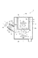
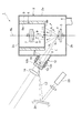
- レーザ光をターゲットに照射することにより、前記ターゲットから活性粒子を発生させ、前記活性粒子を前駆体に付着させるレーザアブレーション装置であって、
前記レーザ光を進入させる光進入口が設けられ、前記ターゲット及び前記前駆体を収容する筐体と、
前記筐体内において前記ターゲットを支持する第1の支持部材と、
前記筐体内において前記第1の支持部材に対向した状態で前記前駆体を支持する第2の支持部材と、
前記第2の支持部材に支持された前記前駆体を加熱する第1の加熱手段と、
前記活性粒子を進入させる粒子進入口が設けられ、前記筐体内において前記前駆体及び前記第2の支持部材を包囲する包囲部材と、
一端が前記光進入口に接続されかつ他端が前記筐体外に位置した状態で前記筐体に取り付けられ、前記他端から前記一端に向かって前記レーザ光を通過させる光通路と、
前記光通路の内面に形成された複数の突起と、
前記突起を冷却する第2の冷却手段と、
前記他端を塞ぐ光透過部材と、
前記光通路の外側から前記光透過部材を加熱する第2の加熱手段と、を備えることを特徴とするレーザアブレーション装置。 - 前記包囲部材は、前記筐体に熱的に接続されていることを特徴とする請求項1記載のレーザアブレーション装置。
- 前記包囲部材を冷却する第1の冷却手段をさらに備えることを特徴とする請求項1又は2記載のレーザアブレーション装置。
- 前記ターゲットはセレンからなることを特徴とする請求項1〜3のいずれか一項記載のレーザアブレーション装置。
Priority Applications (1)
| Application Number | Priority Date | Filing Date | Title |
|---|---|---|---|
| JP2010185250A JP5653128B2 (ja) | 2010-08-20 | 2010-08-20 | レーザアブレーション装置 |
Applications Claiming Priority (1)
| Application Number | Priority Date | Filing Date | Title |
|---|---|---|---|
| JP2010185250A JP5653128B2 (ja) | 2010-08-20 | 2010-08-20 | レーザアブレーション装置 |
Publications (2)
| Publication Number | Publication Date |
|---|---|
| JP2012041615A JP2012041615A (ja) | 2012-03-01 |
| JP5653128B2 true JP5653128B2 (ja) | 2015-01-14 |
Family
ID=45898249
Family Applications (1)
| Application Number | Title | Priority Date | Filing Date |
|---|---|---|---|
| JP2010185250A Expired - Fee Related JP5653128B2 (ja) | 2010-08-20 | 2010-08-20 | レーザアブレーション装置 |
Country Status (1)
| Country | Link |
|---|---|
| JP (1) | JP5653128B2 (ja) |
Family Cites Families (11)
| Publication number | Priority date | Publication date | Assignee | Title |
|---|---|---|---|---|
| JPS5842770A (ja) * | 1981-09-09 | 1983-03-12 | Tohoku Richo Kk | 蒸発源からの蒸気流を阻止する装置 |
| JPS6247474A (ja) * | 1985-08-28 | 1987-03-02 | Fujitsu Ltd | 真空成膜装置 |
| JPS62224669A (ja) * | 1986-03-27 | 1987-10-02 | Mitsubishi Electric Corp | レ−ザセラミツクスコ−テイング方法 |
| JPH01259162A (ja) * | 1988-04-11 | 1989-10-16 | Shimadzu Corp | 薄膜製造装置 |
| JPH06293960A (ja) * | 1993-04-07 | 1994-10-21 | Matsushita Electric Ind Co Ltd | レーザアブレーション装置 |
| JPH06322528A (ja) * | 1993-05-06 | 1994-11-22 | Hitachi Ltd | スパッタ方法およびスパッタ装置 |
| US20050067389A1 (en) * | 2003-09-25 | 2005-03-31 | Greer James A. | Target manipulation for pulsed laser deposition |
| JP2006233266A (ja) * | 2005-02-24 | 2006-09-07 | Fujikura Ltd | 薄膜形成装置 |
| JP2007146265A (ja) * | 2005-11-30 | 2007-06-14 | Seiko Epson Corp | 蒸着装置 |
| JP4370408B2 (ja) * | 2006-03-31 | 2009-11-25 | 国立大学法人 大分大学 | レーザーアブレーション成膜装置 |
| JP2010121204A (ja) * | 2008-10-22 | 2010-06-03 | Fujikura Ltd | 成膜方法及び成膜装置 |
-
2010
- 2010-08-20 JP JP2010185250A patent/JP5653128B2/ja not_active Expired - Fee Related
Also Published As
| Publication number | Publication date |
|---|---|
| JP2012041615A (ja) | 2012-03-01 |
Similar Documents
| Publication | Publication Date | Title |
|---|---|---|
| CN113227443B (zh) | 涂覆设备、处理腔室和涂覆基板的方法以及用至少一个材料层涂覆的基板 | |
| JP4842039B2 (ja) | 蒸発源及びそれを用いた薄膜蒸着方法 | |
| TWI410751B (zh) | 具有清潔配置之光學系統 | |
| JP7122367B2 (ja) | 局所熱処理による多層グラフェンペリクルの同時両面コーティング | |
| TW201127214A (en) | System, method and apparatus for laser produced plasma extreme ultraviolet chamber with hot walls and cold collector mirror | |
| TW200814858A (en) | A method of increasing the conversion efficiency of an EUV and/or soft X-ray lamp and a corresponding apparatus | |
| JP2008248362A (ja) | セレン蒸着装置 | |
| WO2003063181A1 (fr) | Procede et dispositif pour la production de radio-isotopes a partir d'une cible | |
| JP5653128B2 (ja) | レーザアブレーション装置 | |
| JP6176138B2 (ja) | デブリ低減装置 | |
| JP6075096B2 (ja) | ホイルトラップおよびこのホイルトラップを用いた光源装置 | |
| JP2013503969A (ja) | 気相から基板を被覆するための方法及び装置 | |
| JP3788835B2 (ja) | 有機薄膜製造方法 | |
| JP2005083862A (ja) | 光学薄膜およびこれを用いたミラー | |
| TWI877377B (zh) | 極紫外光光源裝置 | |
| JPH09228032A (ja) | 真空蒸着装置およびその真空蒸着装置を用いた真空蒸着方法 | |
| JP4171017B2 (ja) | 加熱装置 | |
| JP4097372B2 (ja) | 高濃度オゾン含有ガスの貯蔵方法と高濃度オゾン含有ガスの貯蔵装置、及び酸化処理方法と酸化処理装置 | |
| JP4056529B2 (ja) | 成膜装置 | |
| US20250101592A1 (en) | Coating apparatus, process chamber, and method of coating a substrate and substrate coated with at least one material layer | |
| JP2006344718A (ja) | 異物除去方法 | |
| JP6065710B2 (ja) | 回転式ホイルトラップ及びこのホイルトラップを用いた光源装置 | |
| JP2009173485A (ja) | 浮遊帯域溶融装置 | |
| JP2004024953A (ja) | 微粒子および微粒子の製造方法 | |
| JP2004315911A (ja) | 蒸発装置、蒸発方法及びそれによる生成物 |
Legal Events
| Date | Code | Title | Description |
|---|---|---|---|
| A621 | Written request for application examination |
Free format text: JAPANESE INTERMEDIATE CODE: A621 Effective date: 20130426 |
|
| A977 | Report on retrieval |
Free format text: JAPANESE INTERMEDIATE CODE: A971007 Effective date: 20140116 |
|
| A131 | Notification of reasons for refusal |
Free format text: JAPANESE INTERMEDIATE CODE: A131 Effective date: 20140121 |
|
| A521 | Request for written amendment filed |
Free format text: JAPANESE INTERMEDIATE CODE: A523 Effective date: 20140319 |
|
| A131 | Notification of reasons for refusal |
Free format text: JAPANESE INTERMEDIATE CODE: A131 Effective date: 20140610 |
|
| A521 | Request for written amendment filed |
Free format text: JAPANESE INTERMEDIATE CODE: A523 Effective date: 20140701 |
|
| TRDD | Decision of grant or rejection written | ||
| A01 | Written decision to grant a patent or to grant a registration (utility model) |
Free format text: JAPANESE INTERMEDIATE CODE: A01 Effective date: 20141028 |
|
| A61 | First payment of annual fees (during grant procedure) |
Free format text: JAPANESE INTERMEDIATE CODE: A61 Effective date: 20141118 |
|
| R150 | Certificate of patent or registration of utility model |
Ref document number: 5653128 Country of ref document: JP Free format text: JAPANESE INTERMEDIATE CODE: R150 |
|
| LAPS | Cancellation because of no payment of annual fees |