JP5675122B2 - 光モジュール - Google Patents
光モジュール Download PDFInfo
- Publication number
- JP5675122B2 JP5675122B2 JP2010019362A JP2010019362A JP5675122B2 JP 5675122 B2 JP5675122 B2 JP 5675122B2 JP 2010019362 A JP2010019362 A JP 2010019362A JP 2010019362 A JP2010019362 A JP 2010019362A JP 5675122 B2 JP5675122 B2 JP 5675122B2
- Authority
- JP
- Japan
- Prior art keywords
- ground conductor
- open stub
- modulation control
- optical module
- via hole
- Prior art date
- Legal status (The legal status is an assumption and is not a legal conclusion. Google has not performed a legal analysis and makes no representation as to the accuracy of the status listed.)
- Active
Links
Images


Classifications
-
- G—PHYSICS
- G02—OPTICS
- G02F—OPTICAL DEVICES OR ARRANGEMENTS FOR THE CONTROL OF LIGHT BY MODIFICATION OF THE OPTICAL PROPERTIES OF THE MEDIA OF THE ELEMENTS INVOLVED THEREIN; NON-LINEAR OPTICS; FREQUENCY-CHANGING OF LIGHT; OPTICAL LOGIC ELEMENTS; OPTICAL ANALOGUE/DIGITAL CONVERTERS
- G02F1/00—Devices or arrangements for the control of the intensity, colour, phase, polarisation or direction of light arriving from an independent light source, e.g. switching, gating or modulating; Non-linear optics
- G02F1/01—Devices or arrangements for the control of the intensity, colour, phase, polarisation or direction of light arriving from an independent light source, e.g. switching, gating or modulating; Non-linear optics for the control of the intensity, phase, polarisation or colour
- G02F1/0121—Operation of devices; Circuit arrangements, not otherwise provided for in this subclass
-
- G—PHYSICS
- G02—OPTICS
- G02F—OPTICAL DEVICES OR ARRANGEMENTS FOR THE CONTROL OF LIGHT BY MODIFICATION OF THE OPTICAL PROPERTIES OF THE MEDIA OF THE ELEMENTS INVOLVED THEREIN; NON-LINEAR OPTICS; FREQUENCY-CHANGING OF LIGHT; OPTICAL LOGIC ELEMENTS; OPTICAL ANALOGUE/DIGITAL CONVERTERS
- G02F1/00—Devices or arrangements for the control of the intensity, colour, phase, polarisation or direction of light arriving from an independent light source, e.g. switching, gating or modulating; Non-linear optics
- G02F1/01—Devices or arrangements for the control of the intensity, colour, phase, polarisation or direction of light arriving from an independent light source, e.g. switching, gating or modulating; Non-linear optics for the control of the intensity, phase, polarisation or colour
- G02F1/03—Devices or arrangements for the control of the intensity, colour, phase, polarisation or direction of light arriving from an independent light source, e.g. switching, gating or modulating; Non-linear optics for the control of the intensity, phase, polarisation or colour based on ceramics or electro-optical crystals, e.g. exhibiting Pockels effect or Kerr effect
- G02F1/035—Devices or arrangements for the control of the intensity, colour, phase, polarisation or direction of light arriving from an independent light source, e.g. switching, gating or modulating; Non-linear optics for the control of the intensity, phase, polarisation or colour based on ceramics or electro-optical crystals, e.g. exhibiting Pockels effect or Kerr effect in an optical waveguide structure
- G02F1/0356—Devices or arrangements for the control of the intensity, colour, phase, polarisation or direction of light arriving from an independent light source, e.g. switching, gating or modulating; Non-linear optics for the control of the intensity, phase, polarisation or colour based on ceramics or electro-optical crystals, e.g. exhibiting Pockels effect or Kerr effect in an optical waveguide structure controlled by a high-frequency electromagnetic wave component in an electric waveguide structure
-
- G—PHYSICS
- G02—OPTICS
- G02F—OPTICAL DEVICES OR ARRANGEMENTS FOR THE CONTROL OF LIGHT BY MODIFICATION OF THE OPTICAL PROPERTIES OF THE MEDIA OF THE ELEMENTS INVOLVED THEREIN; NON-LINEAR OPTICS; FREQUENCY-CHANGING OF LIGHT; OPTICAL LOGIC ELEMENTS; OPTICAL ANALOGUE/DIGITAL CONVERTERS
- G02F1/00—Devices or arrangements for the control of the intensity, colour, phase, polarisation or direction of light arriving from an independent light source, e.g. switching, gating or modulating; Non-linear optics
- G02F1/01—Devices or arrangements for the control of the intensity, colour, phase, polarisation or direction of light arriving from an independent light source, e.g. switching, gating or modulating; Non-linear optics for the control of the intensity, phase, polarisation or colour
- G02F1/21—Devices or arrangements for the control of the intensity, colour, phase, polarisation or direction of light arriving from an independent light source, e.g. switching, gating or modulating; Non-linear optics for the control of the intensity, phase, polarisation or colour by interference
- G02F1/225—Devices or arrangements for the control of the intensity, colour, phase, polarisation or direction of light arriving from an independent light source, e.g. switching, gating or modulating; Non-linear optics for the control of the intensity, phase, polarisation or colour by interference in an optical waveguide structure
- G02F1/2255—Devices or arrangements for the control of the intensity, colour, phase, polarisation or direction of light arriving from an independent light source, e.g. switching, gating or modulating; Non-linear optics for the control of the intensity, phase, polarisation or colour by interference in an optical waveguide structure controlled by a high-frequency electromagnetic component in an electric waveguide structure
Landscapes
- Physics & Mathematics (AREA)
- Nonlinear Science (AREA)
- General Physics & Mathematics (AREA)
- Optics & Photonics (AREA)
- Electromagnetism (AREA)
- Chemical & Material Sciences (AREA)
- Engineering & Computer Science (AREA)
- Ceramic Engineering (AREA)
- Crystallography & Structural Chemistry (AREA)
- Optical Modulation, Optical Deflection, Nonlinear Optics, Optical Demodulation, Optical Logic Elements (AREA)
- Production Of Multi-Layered Print Wiring Board (AREA)
- Semiconductor Lasers (AREA)
Description
図1は、本発明の実施形態に係る光モジュールである光送受信機2の外観図である。同図に示すように、光送受信機には2つのブッシュ3,5が備えられ、各ブッシュには図示してない光ファイバが接続される。本実施形態の場合、ブッシュ3を介して光信号が受信され、ブッシュ5を介して光信号が送信されるようになっている。なお、ブッシュ3,5の材質は、例えば導電性ゴムである。
この光送受信機2では、光変調器モジュール6により位相変調と強度変調とが行われる。例えば、光送受信機2が43Gbpsのビットレートで動作するRZ−DQPSK(Return to Zero Differential Quadrature Phase Shift Keying)方式の光送受信機である場合、RZ−DQPSK変調が行われる。
次に、本発明の実施形態に係る光モジュールである強度変調制御部14について説明する。
次に多層プリント基板16の詳細について説明する。多層プリント基板16は、配線層である銅箔パタンを複数含む多層基板であり、各配線層の間の誘電体の材質は、例えば、FR4(Flame Retardant Type 4)である。配線層は、配線膜とも呼ばれる。
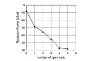
ところで、発明者の検討によると、クロック周波数が21.5GHzと大きい場合、マイクロストリップライン26aと同軸コネクタ18との接続部分から多量の電磁波が放射されるため、電磁波妨害(いわゆるEMI)の発生を防止すべく、強度変調制御部14からの電磁波の放射を抑制する必要があることがわかっている。
この点、この光送受信機2では、配線層34aと配線層34bとの間の配線層にオープンスタブ32が設けられているので(図5参照)、このオープンスタブ32と、配線層34aと、配線層34bと、により、「オープンスタブ32の長さRをn(nは奇数)分の4倍した長さの波長」を有する電磁波を減衰させる帯域阻止フィルタが構成されるようになっている。そのため、「オープンスタブ32の長さRをn(nは奇数)分の4倍した長さの波長」を有する電磁波が配線層34bの開口部30から下方へと放射されたり、「オープンスタブ32の長さRをn(nは奇数)分の4倍した長さの波長」を有する電磁波がバイアホール31を介して下方へと放射されたりすることが抑制される。さらに、配線層34bと配線層34cとの間の配線層にもオープンスタブ32が設けられているので(図5参照)、このオープンスタブ32と、配線層34bと、配線層34cと、によっても、上記の帯域阻止フィルタが構成されるようになっている。そのため、「オープンスタブ32の長さRをn(nは奇数)分の4倍した長さの波長」を有する電磁波が配線層34cの開口部30から下方へと放射されることも抑制されるだけでなく、「オープンスタブ32の長さRをn(nは奇数)分の4倍した長さの波長」を有する電磁波がバイアホール31を介して下方へと放射されたりすることがさらに抑制される。
Claims (7)
- 複数の接地導体層を含む多層プリント基板であって、前記複数の接地導体層すべてに亘って設けられたアンチパッドによって前記複数の接地導体層と絶縁されているバイアホールが形成された多層プリント基板と、
前記多層プリント基板に設置された同軸コネクタと、
光変調器による光変調を制御するための高周波クロック信号を生成し、前記同軸コネクタへと出力する変調制御回路と、
前記多層プリント基板上に形成された信号ラインであって、前記同軸コネクタと、前記多層プリント基板に設置された前記変調制御回路と、に接続された信号ラインと、
前記変調制御回路を覆う金属ケースと、
を含み、
前記複数の接地導体層は、第1の接地導体層と第2の接地導体層とを含み、
前記バイアホールから伸びるオープンスタブが、前記第1の接地導体層と前記第2の接地導体層との間の層に設けられていること、
を特徴とする光モジュール。 - 前記オープンスタブの長さが、前記高周波クロック信号の周波数に応じた長さであること、
を特徴とする請求項1に記載の光モジュール。 - 前記オープンスタブの長さが、前記周波数に基づいて定まる前記高周波クロック信号に対応する波長、を4分のn(nは奇数)倍した長さであること、
を特徴とする請求項2に記載の光モジュール。 - 高周波クロック信号を増幅し、出力する出力端子を備えた増幅ICと、
同軸コネクタと、
前記増幅ICと前記同軸コネクタとを一方の面に搭載し、前記増幅ICの前記出力端子と前記同軸コネクタの中心導体とを接続する信号ラインを備えた多層プリント基板と、
前記多層プリント基板の前記一方の面に設けられ、前記同軸コネクタと前記増幅ICを覆う金属ケースと、を備え、
前記プリント基板は、第1および第2の接地導体層を含む、複数の接地導体層を備え、
前記一方の面に対して垂直となる方向に前記複数の接地導体層すべてを貫くバイアホールが形成されており、かつ前記バイアホールは前記金属ケースの下部領域に配置されており、
前記バイアホールと前記複数の接地導体層とはアンチパッドにより電気的に絶縁されており、
前記バイアホールに接続したオープンスタブが前記第1および前記第2の接地導体層との間に位置して設けられ、
前記オープンスタブの長さは、前記高周波クロック信号の周波数に対応する波長を4分のn(nは奇数)倍した長さであること、と特徴とした光モジュール。 - 請求項1に記載の光モジュールにおいて、
前記多層プリント基板の、前記金属ケースの下部領域に、前記複数の接地導体層および前記信号ラインと絶縁されている前記バイアホールが複数形成され、
前記複数のバイアホールそれぞれから伸びる前記オープンスタブが前記第1の接地導体層と前記第2の接地導体層との間の層に設けられ、前記オープンスタブは扇形形状、二つの扇形を結合した形状、半円形状、または矩形形状のいずれかの形状であること、を特徴とする光モジュール。 - 請求項4または請求項5に記載の光モジュールにおいて、
前記バイアホールから伸びる他のオープンスタブが前記第1の接地導体層と前記第2の接地導体層間以外の他の隣り合う接地導体層間に設けられていること、を特徴とする光モジュール。 - 請求項1ないし請求項6のいずれかに記載の光モジュールにおいて、
前記オープンスタブは、扇形形状、二つの扇形を結合した形状、半円形状、または矩形形状のいずれかの形状であること、を特徴とする光モジュール。
Priority Applications (2)
| Application Number | Priority Date | Filing Date | Title |
|---|---|---|---|
| JP2010019362A JP5675122B2 (ja) | 2010-01-29 | 2010-01-29 | 光モジュール |
| US13/015,769 US8467118B2 (en) | 2010-01-29 | 2011-01-28 | Optical module |
Applications Claiming Priority (1)
| Application Number | Priority Date | Filing Date | Title |
|---|---|---|---|
| JP2010019362A JP5675122B2 (ja) | 2010-01-29 | 2010-01-29 | 光モジュール |
Publications (3)
| Publication Number | Publication Date |
|---|---|
| JP2011159742A JP2011159742A (ja) | 2011-08-18 |
| JP2011159742A5 JP2011159742A5 (ja) | 2012-12-06 |
| JP5675122B2 true JP5675122B2 (ja) | 2015-02-25 |
Family
ID=44341442
Family Applications (1)
| Application Number | Title | Priority Date | Filing Date |
|---|---|---|---|
| JP2010019362A Active JP5675122B2 (ja) | 2010-01-29 | 2010-01-29 | 光モジュール |
Country Status (2)
| Country | Link |
|---|---|
| US (1) | US8467118B2 (ja) |
| JP (1) | JP5675122B2 (ja) |
Families Citing this family (4)
| Publication number | Priority date | Publication date | Assignee | Title |
|---|---|---|---|---|
| JP2010123640A (ja) | 2008-11-17 | 2010-06-03 | Opnext Japan Inc | プリント基板及び光伝送装置 |
| JP5661137B2 (ja) * | 2013-04-11 | 2015-01-28 | 日本オクラロ株式会社 | プリント基板及び光伝送装置 |
| JP6654155B2 (ja) * | 2017-01-10 | 2020-02-26 | Kddi株式会社 | 光伝送システム、ponシステムおよび伝送方法 |
| KR102549519B1 (ko) | 2018-09-25 | 2023-06-29 | 몰렉스 엘엘씨 | 커넥터, 및 표면 접지 평면을 갖는 인쇄 회로 보드 |
Family Cites Families (12)
| Publication number | Priority date | Publication date | Assignee | Title |
|---|---|---|---|---|
| JPH02167525A (ja) * | 1988-12-21 | 1990-06-27 | Fujitsu Ltd | 光変調装置 |
| JPH03198402A (ja) * | 1989-12-26 | 1991-08-29 | Matsushita Electric Ind Co Ltd | マイクロ波回路、バイアス回路及び帯域阻止フィルタ |
| JPH10290075A (ja) * | 1997-04-14 | 1998-10-27 | Murata Mfg Co Ltd | 多層回路基板 |
| JPH10341027A (ja) * | 1997-06-10 | 1998-12-22 | Nippon Telegr & Teleph Corp <Ntt> | 光モジュール |
| JP2004004317A (ja) * | 2002-05-31 | 2004-01-08 | Mitsubishi Electric Corp | 光変調装置 |
| JP2005044963A (ja) * | 2003-07-28 | 2005-02-17 | Tdk Corp | レーザダイオードモジュール |
| JP4633455B2 (ja) * | 2004-12-24 | 2011-02-16 | 富士通セミコンダクター株式会社 | 半導体装置 |
| JP4657860B2 (ja) | 2005-09-16 | 2011-03-23 | 富士通株式会社 | 光送信装置および光通信システム |
| JP2008090093A (ja) * | 2006-10-04 | 2008-04-17 | Nippon Telegr & Teleph Corp <Ntt> | 一心双方向光送受信トランシーバ |
| JP2009129649A (ja) * | 2007-11-21 | 2009-06-11 | Murata Mfg Co Ltd | 基板のコネクタ実装部構造 |
| JP2010123640A (ja) | 2008-11-17 | 2010-06-03 | Opnext Japan Inc | プリント基板及び光伝送装置 |
| JP5334686B2 (ja) * | 2009-05-27 | 2013-11-06 | 三菱電機株式会社 | 多層高周波パッケージ基板 |
-
2010
- 2010-01-29 JP JP2010019362A patent/JP5675122B2/ja active Active
-
2011
- 2011-01-28 US US13/015,769 patent/US8467118B2/en active Active
Also Published As
| Publication number | Publication date |
|---|---|
| JP2011159742A (ja) | 2011-08-18 |
| US8467118B2 (en) | 2013-06-18 |
| US20110188108A1 (en) | 2011-08-04 |
Similar Documents
| Publication | Publication Date | Title |
|---|---|---|
| CN108415182B (zh) | 带fpc的光调制器及使用该光调制器的光发送装置 | |
| JP5216147B2 (ja) | 差動伝送回路、光送受信モジュール、及び情報処理装置 | |
| CN101772859B (zh) | 波导管的连接结构 | |
| JP5859219B2 (ja) | 差動伝送線路、及び通信装置 | |
| US8385748B2 (en) | Printed circuit board and optical transmission device | |
| JP4852442B2 (ja) | 光送信モジュール | |
| US10921620B2 (en) | Optical modulator and optical transmission apparatus | |
| JP5675122B2 (ja) | 光モジュール | |
| CN108206318A (zh) | 印制电路板、光模块、以及光传输装置 | |
| CN107636515A (zh) | 光调制器 | |
| JP5146267B2 (ja) | 配線基板、プリント配線板の製造方法 | |
| JPWO2011102300A1 (ja) | 導波管・平面線路変換器 | |
| JP2008283676A (ja) | 高周波センサ装置 | |
| JP4532509B2 (ja) | 車載電波レーダ装置 | |
| JP2019201197A (ja) | 層間伝送線路 | |
| JP4519086B2 (ja) | パッチアンテナおよび高周波デバイス | |
| CN108700761B (zh) | 带有fpc的光调制器及使用该光调制器的光发送装置 | |
| JP2011003651A (ja) | 回路装置、及び電子機器 | |
| JP5661137B2 (ja) | プリント基板及び光伝送装置 | |
| JP2017143113A (ja) | 電子機器 | |
| WO2022215713A1 (ja) | アンテナ装置 | |
| JP6723754B2 (ja) | 電子機器 | |
| WO2024150551A1 (ja) | 多層基板 | |
| WO2021065459A1 (ja) | 高周波シールド構造 | |
| JP2010199417A (ja) | 電波吸収部材およびシールド蓋部材 |
Legal Events
| Date | Code | Title | Description |
|---|---|---|---|
| A621 | Written request for application examination |
Free format text: JAPANESE INTERMEDIATE CODE: A621 Effective date: 20120312 |
|
| A521 | Request for written amendment filed |
Free format text: JAPANESE INTERMEDIATE CODE: A523 Effective date: 20121024 |
|
| A977 | Report on retrieval |
Free format text: JAPANESE INTERMEDIATE CODE: A971007 Effective date: 20130123 |
|
| A131 | Notification of reasons for refusal |
Free format text: JAPANESE INTERMEDIATE CODE: A131 Effective date: 20130806 |
|
| A521 | Request for written amendment filed |
Free format text: JAPANESE INTERMEDIATE CODE: A523 Effective date: 20131004 |
|
| A131 | Notification of reasons for refusal |
Free format text: JAPANESE INTERMEDIATE CODE: A131 Effective date: 20140218 |
|
| A521 | Request for written amendment filed |
Free format text: JAPANESE INTERMEDIATE CODE: A523 Effective date: 20140418 |
|
| A131 | Notification of reasons for refusal |
Free format text: JAPANESE INTERMEDIATE CODE: A131 Effective date: 20140805 |
|
| A521 | Request for written amendment filed |
Free format text: JAPANESE INTERMEDIATE CODE: A523 Effective date: 20141001 |
|
| TRDD | Decision of grant or rejection written | ||
| A01 | Written decision to grant a patent or to grant a registration (utility model) |
Free format text: JAPANESE INTERMEDIATE CODE: A01 Effective date: 20141216 |
|
| A61 | First payment of annual fees (during grant procedure) |
Free format text: JAPANESE INTERMEDIATE CODE: A61 Effective date: 20141224 |
|
| R150 | Certificate of patent or registration of utility model |
Ref document number: 5675122 Country of ref document: JP Free format text: JAPANESE INTERMEDIATE CODE: R150 |
|
| R250 | Receipt of annual fees |
Free format text: JAPANESE INTERMEDIATE CODE: R250 |
|
| R250 | Receipt of annual fees |
Free format text: JAPANESE INTERMEDIATE CODE: R250 |
|
| S533 | Written request for registration of change of name |
Free format text: JAPANESE INTERMEDIATE CODE: R313533 |
|
| R350 | Written notification of registration of transfer |
Free format text: JAPANESE INTERMEDIATE CODE: R350 |
|
| R250 | Receipt of annual fees |
Free format text: JAPANESE INTERMEDIATE CODE: R250 |
|
| R250 | Receipt of annual fees |
Free format text: JAPANESE INTERMEDIATE CODE: R250 |
|
| R250 | Receipt of annual fees |
Free format text: JAPANESE INTERMEDIATE CODE: R250 |
|
| R250 | Receipt of annual fees |
Free format text: JAPANESE INTERMEDIATE CODE: R250 |
|
| R250 | Receipt of annual fees |
Free format text: JAPANESE INTERMEDIATE CODE: R250 |
|
| R250 | Receipt of annual fees |
Free format text: JAPANESE INTERMEDIATE CODE: R250 |
|
| R250 | Receipt of annual fees |
Free format text: JAPANESE INTERMEDIATE CODE: R250 |