JP5676659B2 - 半田付け方法 - Google Patents
半田付け方法 Download PDFInfo
- Publication number
- JP5676659B2 JP5676659B2 JP2013002777A JP2013002777A JP5676659B2 JP 5676659 B2 JP5676659 B2 JP 5676659B2 JP 2013002777 A JP2013002777 A JP 2013002777A JP 2013002777 A JP2013002777 A JP 2013002777A JP 5676659 B2 JP5676659 B2 JP 5676659B2
- Authority
- JP
- Japan
- Prior art keywords
- pad
- area
- cable
- solder ball
- inner conductor
- Prior art date
- Legal status (The legal status is an assumption and is not a legal conclusion. Google has not performed a legal analysis and makes no representation as to the accuracy of the status listed.)
- Expired - Fee Related
Links
Images



Landscapes
- Electric Connection Of Electric Components To Printed Circuits (AREA)
Description
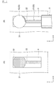
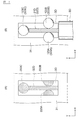
12、121A、121B、122A、122B、123A、123B、123C・・・半田ボール
21、21B、21C、21D・・・内部導体
3、3B、3C、3D・・・パッド
Claims (1)
- 半田ボールが設けられたパッド上に導電線を載置して、前記パッド上での前記導電線の位置を前記半田ボールによって規定し、前記半田ボールを溶融させることにより前記導電線を前記パッドに半田付けする半田付け方法であって、
前記パッドは、
前記パッドの平坦面に設けられ、前記導電線が載置される第1のエリアと、
前記平坦面に一箇所のみ設けられ、前記半田ボールが設けられた第2のエリアと、を有し、
前記第1のエリアと前記第2のエリアは、相互に独立して設けられており、
前記第2のエリアは、前記パッドの長手方向に沿って前記第1のエリアの先端部に隣り合うように設けられていることを特徴とする半田付け方法。
Priority Applications (1)
| Application Number | Priority Date | Filing Date | Title |
|---|---|---|---|
| JP2013002777A JP5676659B2 (ja) | 2013-01-10 | 2013-01-10 | 半田付け方法 |
Applications Claiming Priority (1)
| Application Number | Priority Date | Filing Date | Title |
|---|---|---|---|
| JP2013002777A JP5676659B2 (ja) | 2013-01-10 | 2013-01-10 | 半田付け方法 |
Publications (2)
| Publication Number | Publication Date |
|---|---|
| JP2014135392A JP2014135392A (ja) | 2014-07-24 |
| JP5676659B2 true JP5676659B2 (ja) | 2015-02-25 |
Family
ID=51413471
Family Applications (1)
| Application Number | Title | Priority Date | Filing Date |
|---|---|---|---|
| JP2013002777A Expired - Fee Related JP5676659B2 (ja) | 2013-01-10 | 2013-01-10 | 半田付け方法 |
Country Status (1)
| Country | Link |
|---|---|
| JP (1) | JP5676659B2 (ja) |
Families Citing this family (1)
| Publication number | Priority date | Publication date | Assignee | Title |
|---|---|---|---|---|
| JP2017103278A (ja) | 2015-11-30 | 2017-06-08 | キヤノン株式会社 | プリント配線板、該プリント配線板を備えた電子機器及び該プリント配線板における半田付け方法 |
Family Cites Families (3)
| Publication number | Priority date | Publication date | Assignee | Title |
|---|---|---|---|---|
| JPH10326956A (ja) * | 1997-05-27 | 1998-12-08 | Fujitsu Ltd | プリント配線板、該プリント配線板の製造方法及び該プリント配線板への電子部品の実装方法 |
| JP3308934B2 (ja) * | 1999-06-22 | 2002-07-29 | 九州日本電気株式会社 | 樹脂モールドbga型半導体装置の製造方法 |
| JP5738623B2 (ja) * | 2011-02-22 | 2015-06-24 | オリンパス株式会社 | ケーブル接続構造およびケーブル接続方法 |
-
2013
- 2013-01-10 JP JP2013002777A patent/JP5676659B2/ja not_active Expired - Fee Related
Also Published As
| Publication number | Publication date |
|---|---|
| JP2014135392A (ja) | 2014-07-24 |
Similar Documents
| Publication | Publication Date | Title |
|---|---|---|
| US8900007B2 (en) | Cable connector and cable assembly, and method of manufacturing cable assembly | |
| CN101336042A (zh) | 焊盘、具有该焊盘的电路板和电子装置 | |
| TW200937782A (en) | Connection structure and connection method of coaxial cable harness | |
| JP4983687B2 (ja) | シールドの電気的接続方法 | |
| JP5676659B2 (ja) | 半田付け方法 | |
| KR100715410B1 (ko) | 혼성 집적 회로 | |
| WO2021039325A1 (ja) | モジュール | |
| JP2017139394A (ja) | 電子回路基板とfpcの電気接続構造および方法 | |
| US20220386468A1 (en) | Semiconductor module and electronic apparatus | |
| CN107079588B (zh) | 印刷基板、印刷基板的制造方法以及导电性部件的接合方法 | |
| JP3163214U (ja) | 半導体装置 | |
| JP2005116685A (ja) | プリント配線基板、電子部品モジュール及び電子機器 | |
| JP2008112636A (ja) | 多心同軸ケーブルおよびその製造方法 | |
| US7633016B2 (en) | Coupling structure between circuit board and frame member | |
| TWI391056B (zh) | 焊盤、具有該焊盤的電路板和電子裝置 | |
| US12256491B2 (en) | Electronic component mounting substrate, electronic component mounted body, and method of manufacturing the same, as well as electronic apparatus | |
| JP7690325B2 (ja) | 半導体モジュールおよび電子機器 | |
| KR20130074490A (ko) | 인쇄회로기판 사이의 연결 구조 | |
| JP2017147396A (ja) | 基板装置の製造方法及び基板装置 | |
| JP4828361B2 (ja) | 電気接点への半田上がり防止方法及び該防止方法を用いた電気接点 | |
| JP2014135206A (ja) | 半田付け方法 | |
| JP2002151627A (ja) | 半導体装置、その製造方法および実装方法 | |
| CN110087387A (zh) | 接合位置准确性被改善的柔性电路板 | |
| JP2751897B2 (ja) | ボールグリッドアレイ実装構造及び実装方法 | |
| JP3092973U (ja) | 面実装型電子回路ユニット |
Legal Events
| Date | Code | Title | Description |
|---|---|---|---|
| A131 | Notification of reasons for refusal |
Free format text: JAPANESE INTERMEDIATE CODE: A131 Effective date: 20140715 |
|
| A521 | Written amendment |
Free format text: JAPANESE INTERMEDIATE CODE: A523 Effective date: 20140911 |
|
| A131 | Notification of reasons for refusal |
Free format text: JAPANESE INTERMEDIATE CODE: A131 Effective date: 20141007 |
|
| A521 | Written amendment |
Free format text: JAPANESE INTERMEDIATE CODE: A523 Effective date: 20141121 |
|
| TRDD | Decision of grant or rejection written | ||
| A01 | Written decision to grant a patent or to grant a registration (utility model) |
Free format text: JAPANESE INTERMEDIATE CODE: A01 Effective date: 20141216 |
|
| A61 | First payment of annual fees (during grant procedure) |
Free format text: JAPANESE INTERMEDIATE CODE: A61 Effective date: 20141225 |
|
| R151 | Written notification of patent or utility model registration |
Ref document number: 5676659 Country of ref document: JP Free format text: JAPANESE INTERMEDIATE CODE: R151 |
|
| R250 | Receipt of annual fees |
Free format text: JAPANESE INTERMEDIATE CODE: R250 |
|
| R250 | Receipt of annual fees |
Free format text: JAPANESE INTERMEDIATE CODE: R250 |
|
| LAPS | Cancellation because of no payment of annual fees |