JP5898657B2 - 不揮発性半導体記憶装置 - Google Patents
不揮発性半導体記憶装置 Download PDFInfo
- Publication number
- JP5898657B2 JP5898657B2 JP2013180932A JP2013180932A JP5898657B2 JP 5898657 B2 JP5898657 B2 JP 5898657B2 JP 2013180932 A JP2013180932 A JP 2013180932A JP 2013180932 A JP2013180932 A JP 2013180932A JP 5898657 B2 JP5898657 B2 JP 5898657B2
- Authority
- JP
- Japan
- Prior art keywords
- source line
- memory
- monitor position
- voltage
- source
- Prior art date
- Legal status (The legal status is an assumption and is not a legal conclusion. Google has not performed a legal analysis and makes no representation as to the accuracy of the status listed.)
- Expired - Fee Related
Links
Images








Classifications
-
- G—PHYSICS
- G11—INFORMATION STORAGE
- G11C—STATIC STORES
- G11C16/00—Erasable programmable read-only memories
- G11C16/02—Erasable programmable read-only memories electrically programmable
- G11C16/06—Auxiliary circuits, e.g. for writing into memory
- G11C16/26—Sensing or reading circuits; Data output circuits
-
- G—PHYSICS
- G11—INFORMATION STORAGE
- G11C—STATIC STORES
- G11C16/00—Erasable programmable read-only memories
- G11C16/02—Erasable programmable read-only memories electrically programmable
- G11C16/04—Erasable programmable read-only memories electrically programmable using variable threshold transistors, e.g. FAMOS
- G11C16/0483—Erasable programmable read-only memories electrically programmable using variable threshold transistors, e.g. FAMOS comprising cells having several storage transistors connected in series
-
- G—PHYSICS
- G11—INFORMATION STORAGE
- G11C—STATIC STORES
- G11C16/00—Erasable programmable read-only memories
- G11C16/02—Erasable programmable read-only memories electrically programmable
- G11C16/06—Auxiliary circuits, e.g. for writing into memory
- G11C16/34—Determination of programming status, e.g. threshold voltage, overprogramming or underprogramming, retention
- G11C16/3418—Disturbance prevention or evaluation; Refreshing of disturbed memory data
-
- H—ELECTRICITY
- H10—SEMICONDUCTOR DEVICES; ELECTRIC SOLID-STATE DEVICES NOT OTHERWISE PROVIDED FOR
- H10B—ELECTRONIC MEMORY DEVICES
- H10B43/00—EEPROM devices comprising charge-trapping gate insulators
- H10B43/20—EEPROM devices comprising charge-trapping gate insulators characterised by three-dimensional [3D] arrangements, e.g. with cells on different height levels
- H10B43/23—EEPROM devices comprising charge-trapping gate insulators characterised by three-dimensional [3D] arrangements, e.g. with cells on different height levels with source and drain on different levels, e.g. with sloping channels
- H10B43/27—EEPROM devices comprising charge-trapping gate insulators characterised by three-dimensional [3D] arrangements, e.g. with cells on different height levels with source and drain on different levels, e.g. with sloping channels the channels comprising vertical portions, e.g. U-shaped channels
Landscapes
- Engineering & Computer Science (AREA)
- Microelectronics & Electronic Packaging (AREA)
- Semiconductor Memories (AREA)
- Read Only Memory (AREA)
- Non-Volatile Memory (AREA)
Description
本実施形態の不揮発性半導体記憶装置について、図1乃至図8を参照して説明する。図1は本実施形態の不揮発性半導体記憶装置を示すブロック図である。図2は不揮発性半導体記憶装置のメモリセルアレイを示すブロック図である。図3はメモリセルアレイを示す断面図である。
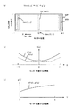
図17はソース線電圧の面内分布のシミュレーション方法を説明するための図で、図17(a)はメモリプレーンMP内のX、Y座標の定義を示す図、図17(b)はX方向の電圧分布を表わす関数を模式的に示す図、図17(c)はY方向の電圧分布を表わす関数を模式的に示す図である。
Vsrc(x、y)=f(x)+g(y)
図17(b)に示すように、比較例の関数f2(x)は原点から両端に向かって対称に単調増加し、下凸のカーブを描くとする。一方、本実施形態の関数f1(x)は中間から一端および中央に向かって単調増加し、W型のカーブを描くとする。
本実施形態に係る不揮発性半導体記憶装置について、図21および図22を用いて説明する。図21は本実施形態の不揮発性半導体記憶装置のメモリセルアレイを含む周辺回路を示すブロック図、図22はソース線の電圧分布のモデルを示す図である。
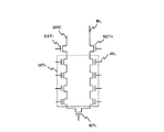
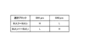
本実施形態に係る不揮発性半導体記憶装置について、図23乃至図25を用いて説明する。図23は本実施形態の不揮発性半導体記憶装置のソース線制御回路を示す図、図24はデコード回路のデコード結果を示す図、図25はスイッチ回路を示す図である。
(付記1) 複数の前記第1ソース線は第1ピッチで前記ビット線方向に配列され、複数の前記第2ソース線は第2ピッチで前記ワード線方向に配列され、複数の前記第3ソース線は第3ピッチで前記ビット線方向に配列され、前記第2ピッチおよび前記第3ピッチは前記第1ピッチより大きい請求項1に記載の不揮発性半導体記憶装置。
11、61、100 ソース線制御回路
12 ワード線ドライバ
13、13a ロウデコーダ
14 センスアンプ
15 データラッチ
16 データ入出力バッファ
17 アドレスバッファ
18 電圧生成回路
19 外部コントローラ
20、20a ソース線ドライバ
21、62 ソース線モニター位置選択回路
22ソース線電圧制御回路
23、63 デコード回路
24、64 スイッチ回路
24a NOR回路
24b、STr、STrC、STrE MOSトランジスタ
30 バックゲート層
32 メモリ層
34 選択トランジスタ層
36 配線層
40、43 柱状半導体層
41、42 コンタクトプラグ
46 シャント
MA メモリセルアレイ
MB メモリブロック
MP メモリプレーン
MS メモリストリング
BTr バックゲートトランジスタ
MTr メモリトランジスタ
SDTr、SSTr 選択トランジスタ
N0、N1、N2、M3 接続ノード(ソース線モニター位置)
MON0、MON1、MON2、MON3 モニター配線
WL ワード線
BL ビット線
SRC ソース線
D0 第1配線層
D1 第2配線層
D2 第3配線層
C1 第1コンタクト
C2 第2コンタクト
Vbl ビット線電圧
Vsrc ソース線電圧
Vref 基準電圧
MP1 第1の領域
MP2 第2の領域
MP3 第3の領域
Sc 選択信号
LS1、LS2、LS3 レベルシフト回路
SW1、SW2、SW3 スイッチ素子
Rsrc1、Rsrc2 配線抵抗
Vu1、Vu2、Vu3、Vu4、Vu5 ソース線の浮き
B1、B2 境界
Claims (6)
- 複数のメモリトランジスタを含む複数のメモリストリングと、
複数の前記メモリストリングの一端にそれぞれ接続された複数の第1ソース線と、
前記第1ソース線の上方に設けられ、前記第1ソース線に電気的に接続された複数の第2ソース線と、
前記第2ソース線の上方に設けられ、前記第2ソース線に電気的に接続された複数の第3ソース線と、
複数の前記第3ソース線と基準端子との間にそれぞれ接続された複数のトランジスタを有し、前記複数のトランジスタのゲート電極が互いに接続されたソース線ドライバと、
複数の前記第3ソース線に設けられた第1モニター位置に接続された第1配線と、
複数の前記第3ソース線に設けられ、前記第1モニター位置と異なる第2モニター位置に接続された第2配線と、
前記第1モニター位置または前記第2モニター位置を選択する選択回路と、
前記選択回路と前記ソース線ドライバとの間に接続され、選択された前記第1モニター位置または前記第2モニター位置のソース線電圧と基準電圧とを比較し、前記比較結果を前記ソース線ドライバに出力するソース線電圧制御回路と、
を具備することを特徴とする不揮発性半導体記憶装置。 - 前記選択回路に入力され、前記第1モニター位置または前記第2モニター位置を選択するための選択信号は、データを読み出すまたは書き込むまたは消去するために選択された前記メモリストリングの属するメモリブロックのアドレス、または選択された前記メモリストリングのアドレスを含み、
前記選択回路は、前記メモリブロックのアドレス、または前記メモリストリングのアドレスをデコードして、前記第1モニター位置および前記第2モニター位置にそれぞれ対応したハイレベル信号またはロウレベル信号を出力するデコード回路と、
一端が前記第1配線および前記第2配線にそれぞれ接続され、他端が共通接続され、前記ハイレベル信号またはロウレベル信号に応じてオンまたはオフする複数のスイッチ素子を有するスイッチ回路と、
を具備することを特徴とする請求項1に記載の不揮発性半導体記憶装置。 - 前記ソース線電圧制御回路は、
選択された前記第1モニター位置または前記第2モニター位置におけるソース線電圧が入力される非反転端子と、
前記基準電圧が入力される反転端子と、
前記比較結果を出力する出力端子と、
を有する差動回路であることを特徴とする請求項1に記載の不揮発性半導体記憶装置。 - 前記選択回路は、データを読み出すまたは書き込むまたは消去するために選択された前記メモリストリングの属するメモリブロックのアドレス、または選択された前記メモリストリングのアドレスに基づいて、前記第1モニター位置または前記第2モニター位置を選択されたメモリストリングの物理的位置に近づけるように、前記第1配線または前記第2配線を選択することを特徴とする請求項1に記載の不揮発性半導体記憶装置。
- 前記第1モニター位置および前記第2モニター位置は、前記ソース線ドライバの上方に設けられていることを特徴とする請求項1に記載の不揮発性半導体記憶装置。
- 複数の前記ソース線ドライバを有し、複数の前記ソース線ドライバが前記メモリセルアレイのワード線方向に沿って分散して配置されていることを特徴とする請求項1に記載の不揮発性半導体記憶装置。
Priority Applications (2)
| Application Number | Priority Date | Filing Date | Title |
|---|---|---|---|
| JP2013180932A JP5898657B2 (ja) | 2013-09-02 | 2013-09-02 | 不揮発性半導体記憶装置 |
| US14/194,608 US9053807B2 (en) | 2013-09-02 | 2014-02-28 | Non-volatile semiconductor memory device |
Applications Claiming Priority (1)
| Application Number | Priority Date | Filing Date | Title |
|---|---|---|---|
| JP2013180932A JP5898657B2 (ja) | 2013-09-02 | 2013-09-02 | 不揮発性半導体記憶装置 |
Publications (2)
| Publication Number | Publication Date |
|---|---|
| JP2015049916A JP2015049916A (ja) | 2015-03-16 |
| JP5898657B2 true JP5898657B2 (ja) | 2016-04-06 |
Family
ID=52583069
Family Applications (1)
| Application Number | Title | Priority Date | Filing Date |
|---|---|---|---|
| JP2013180932A Expired - Fee Related JP5898657B2 (ja) | 2013-09-02 | 2013-09-02 | 不揮発性半導体記憶装置 |
Country Status (2)
| Country | Link |
|---|---|
| US (1) | US9053807B2 (ja) |
| JP (1) | JP5898657B2 (ja) |
Families Citing this family (12)
| Publication number | Priority date | Publication date | Assignee | Title |
|---|---|---|---|---|
| KR20150116175A (ko) * | 2014-04-07 | 2015-10-15 | 에스케이하이닉스 주식회사 | 소스라인 저항 감소를 위한 비휘발성 메모리 장치 |
| KR102293136B1 (ko) * | 2014-10-22 | 2021-08-26 | 삼성전자주식회사 | 비휘발성 메모리 장치, 그것을 포함하는 저장 장치 및 그것의 동작 방법 |
| JP2016170837A (ja) * | 2015-03-12 | 2016-09-23 | 株式会社東芝 | 半導体記憶装置 |
| JP2016225614A (ja) | 2015-05-26 | 2016-12-28 | 株式会社半導体エネルギー研究所 | 半導体装置 |
| JP6433871B2 (ja) * | 2015-09-10 | 2018-12-05 | 東芝メモリ株式会社 | 半導体記憶装置 |
| JP6400547B2 (ja) | 2015-09-14 | 2018-10-03 | 東芝メモリ株式会社 | メモリデバイス |
| US9953719B2 (en) | 2016-05-18 | 2018-04-24 | Silicon Storage Technology, Inc. | Flash memory cell and associated decoders |
| US9786378B1 (en) * | 2016-12-02 | 2017-10-10 | Sandisk Technologies Llc | Equalizing erase depth in different blocks of memory cells |
| US10163494B1 (en) * | 2017-05-31 | 2018-12-25 | Taiwan Semiconductor Manufacturing Co., Ltd. | Memory device and fabrication method thereof |
| JP2019117678A (ja) * | 2017-12-27 | 2019-07-18 | ルネサスエレクトロニクス株式会社 | 半導体装置 |
| JP7091130B2 (ja) | 2018-05-08 | 2022-06-27 | キオクシア株式会社 | 半導体記憶装置 |
| KR102881083B1 (ko) * | 2020-09-23 | 2025-11-06 | 삼성전자주식회사 | 반도체 장치 및 이를 포함하는 전자 시스템 |
Family Cites Families (14)
| Publication number | Priority date | Publication date | Assignee | Title |
|---|---|---|---|---|
| JPH10154803A (ja) * | 1996-11-25 | 1998-06-09 | Toshiba Corp | 不揮発性半導体メモリ |
| JPH1166248A (ja) * | 1997-08-12 | 1999-03-09 | Mitsubishi Electric Corp | 非接触型icカード |
| JP2001195890A (ja) * | 2000-01-12 | 2001-07-19 | Sharp Corp | 不揮発性半導体メモリ装置の書込み方式および書込み回路 |
| JP4326127B2 (ja) * | 2000-07-07 | 2009-09-02 | 株式会社ルネサステクノロジ | 半導体記憶装置 |
| JP5142692B2 (ja) | 2007-12-11 | 2013-02-13 | 株式会社東芝 | 不揮発性半導体記憶装置 |
| US7764547B2 (en) * | 2007-12-20 | 2010-07-27 | Sandisk Corporation | Regulation of source potential to combat cell source IR drop |
| JP5127439B2 (ja) * | 2007-12-28 | 2013-01-23 | 株式会社東芝 | 半導体記憶装置 |
| JP2009238874A (ja) | 2008-03-26 | 2009-10-15 | Toshiba Corp | 半導体メモリ及びその製造方法 |
| JP2009266944A (ja) | 2008-04-23 | 2009-11-12 | Toshiba Corp | 三次元積層不揮発性半導体メモリ |
| JP5283960B2 (ja) | 2008-04-23 | 2013-09-04 | 株式会社東芝 | 三次元積層不揮発性半導体メモリ |
| JP2010123201A (ja) * | 2008-11-20 | 2010-06-03 | Toshiba Corp | 不揮発性半導体記憶装置 |
| JP2011003850A (ja) * | 2009-06-22 | 2011-01-06 | Toshiba Corp | 半導体記憶装置 |
| JP2013004128A (ja) * | 2011-06-14 | 2013-01-07 | Toshiba Corp | 不揮発性半導体記憶装置 |
| JP2013200932A (ja) * | 2012-03-26 | 2013-10-03 | Toshiba Corp | 不揮発性半導体記憶装置 |
-
2013
- 2013-09-02 JP JP2013180932A patent/JP5898657B2/ja not_active Expired - Fee Related
-
2014
- 2014-02-28 US US14/194,608 patent/US9053807B2/en active Active
Also Published As
| Publication number | Publication date |
|---|---|
| US20150063027A1 (en) | 2015-03-05 |
| JP2015049916A (ja) | 2015-03-16 |
| US9053807B2 (en) | 2015-06-09 |
Similar Documents
| Publication | Publication Date | Title |
|---|---|---|
| JP5898657B2 (ja) | 不揮発性半導体記憶装置 | |
| JP4398750B2 (ja) | Nand型フラッシュメモリ | |
| JP4907925B2 (ja) | 不揮発性半導体記憶装置 | |
| US20160322369A1 (en) | Nonvolatile semiconductor memory device | |
| KR100749673B1 (ko) | 불휘발성 반도체 기억 장치 | |
| US10418072B2 (en) | Memories having select devices between access lines and in memory cells | |
| CN105009220B (zh) | 3d存储器中的子块解码 | |
| KR102491576B1 (ko) | 비휘발성 메모리 장치 | |
| JP2015216179A (ja) | 半導体記憶装置 | |
| JP2010134983A (ja) | デプレッションタイプnandフラッシュメモリ | |
| US20160019971A1 (en) | Nonvolatile semiconductor memory device and method of controlling the same | |
| US20140269087A1 (en) | Lithography-friendly Local Read Circuit for NAND Flash Memory Devices and Manufacturing Method Thereof | |
| KR20190113079A (ko) | 복수의 수직 채널 구조체들을 갖는 3차원 메모리 장치 | |
| JP2018049675A (ja) | 半導体記憶装置及びその制御方法 | |
| US11538536B2 (en) | Semiconductor memory device having insulating layers disposed between a plurality of memory string structures | |
| US20150078077A1 (en) | Nonvolatile semiconductor memory device | |
| JP2019114314A (ja) | 半導体記憶装置 | |
| CN104217758A (zh) | 非易失性存储器件 | |
| KR20160097006A (ko) | 반도체 메모리 장치 및 그 프로그램 방법 | |
| US12283315B2 (en) | Semiconductor device and method of controlling the same | |
| US9245628B2 (en) | Non-volatile semiconductor memory device | |
| US9129683B2 (en) | High performance semiconductor memory device that has different page addresses allotted to multiple bits of memory cells | |
| JP5023177B2 (ja) | 半導体記憶装置 | |
| US12112807B2 (en) | Semiconductor storage device | |
| CN108206039A (zh) | 存储器装置与其相关的控制方法 |
Legal Events
| Date | Code | Title | Description |
|---|---|---|---|
| RD01 | Notification of change of attorney |
Free format text: JAPANESE INTERMEDIATE CODE: A7421 Effective date: 20150218 |
|
| A621 | Written request for application examination |
Free format text: JAPANESE INTERMEDIATE CODE: A621 Effective date: 20150821 |
|
| A977 | Report on retrieval |
Free format text: JAPANESE INTERMEDIATE CODE: A971007 Effective date: 20160129 |
|
| TRDD | Decision of grant or rejection written | ||
| A01 | Written decision to grant a patent or to grant a registration (utility model) |
Free format text: JAPANESE INTERMEDIATE CODE: A01 Effective date: 20160205 |
|
| A61 | First payment of annual fees (during grant procedure) |
Free format text: JAPANESE INTERMEDIATE CODE: A61 Effective date: 20160304 |
|
| R151 | Written notification of patent or utility model registration |
Ref document number: 5898657 Country of ref document: JP Free format text: JAPANESE INTERMEDIATE CODE: R151 |
|
| LAPS | Cancellation because of no payment of annual fees |