JP5955246B2 - 半導体装置の製造方法 - Google Patents
半導体装置の製造方法 Download PDFInfo
- Publication number
- JP5955246B2 JP5955246B2 JP2013035300A JP2013035300A JP5955246B2 JP 5955246 B2 JP5955246 B2 JP 5955246B2 JP 2013035300 A JP2013035300 A JP 2013035300A JP 2013035300 A JP2013035300 A JP 2013035300A JP 5955246 B2 JP5955246 B2 JP 5955246B2
- Authority
- JP
- Japan
- Prior art keywords
- substrate
- sic
- semiconductor device
- film
- back surface
- Prior art date
- Legal status (The legal status is an assumption and is not a legal conclusion. Google has not performed a legal analysis and makes no representation as to the accuracy of the status listed.)
- Active
Links
Images




Classifications
-
- H—ELECTRICITY
- H10—SEMICONDUCTOR DEVICES; ELECTRIC SOLID-STATE DEVICES NOT OTHERWISE PROVIDED FOR
- H10P—GENERIC PROCESSES OR APPARATUS FOR THE MANUFACTURE OR TREATMENT OF DEVICES COVERED BY CLASS H10
- H10P95/00—Generic processes or apparatus for manufacture or treatments not covered by the other groups of this subclass
- H10P95/90—Thermal treatments, e.g. annealing or sintering
-
- H—ELECTRICITY
- H10—SEMICONDUCTOR DEVICES; ELECTRIC SOLID-STATE DEVICES NOT OTHERWISE PROVIDED FOR
- H10D—INORGANIC ELECTRIC SEMICONDUCTOR DEVICES
- H10D12/00—Bipolar devices controlled by the field effect, e.g. insulated-gate bipolar transistors [IGBT]
- H10D12/01—Manufacture or treatment
- H10D12/031—Manufacture or treatment of IGBTs
-
- H—ELECTRICITY
- H10—SEMICONDUCTOR DEVICES; ELECTRIC SOLID-STATE DEVICES NOT OTHERWISE PROVIDED FOR
- H10D—INORGANIC ELECTRIC SEMICONDUCTOR DEVICES
- H10D30/00—Field-effect transistors [FET]
- H10D30/01—Manufacture or treatment
- H10D30/021—Manufacture or treatment of FETs having insulated gates [IGFET]
- H10D30/028—Manufacture or treatment of FETs having insulated gates [IGFET] of double-diffused metal oxide semiconductor [DMOS] FETs
- H10D30/0291—Manufacture or treatment of FETs having insulated gates [IGFET] of double-diffused metal oxide semiconductor [DMOS] FETs of vertical DMOS [VDMOS] FETs
-
- H—ELECTRICITY
- H10—SEMICONDUCTOR DEVICES; ELECTRIC SOLID-STATE DEVICES NOT OTHERWISE PROVIDED FOR
- H10D—INORGANIC ELECTRIC SEMICONDUCTOR DEVICES
- H10D30/00—Field-effect transistors [FET]
- H10D30/60—Insulated-gate field-effect transistors [IGFET]
- H10D30/63—Vertical IGFETs
-
- H—ELECTRICITY
- H10—SEMICONDUCTOR DEVICES; ELECTRIC SOLID-STATE DEVICES NOT OTHERWISE PROVIDED FOR
- H10D—INORGANIC ELECTRIC SEMICONDUCTOR DEVICES
- H10D62/00—Semiconductor bodies, or regions thereof, of devices having potential barriers
- H10D62/80—Semiconductor bodies, or regions thereof, of devices having potential barriers characterised by the materials
- H10D62/83—Semiconductor bodies, or regions thereof, of devices having potential barriers characterised by the materials being Group IV materials, e.g. B-doped Si or undoped Ge
- H10D62/832—Semiconductor bodies, or regions thereof, of devices having potential barriers characterised by the materials being Group IV materials, e.g. B-doped Si or undoped Ge being Group IV materials comprising two or more elements, e.g. SiGe
- H10D62/8325—Silicon carbide
-
- H—ELECTRICITY
- H10—SEMICONDUCTOR DEVICES; ELECTRIC SOLID-STATE DEVICES NOT OTHERWISE PROVIDED FOR
- H10P—GENERIC PROCESSES OR APPARATUS FOR THE MANUFACTURE OR TREATMENT OF DEVICES COVERED BY CLASS H10
- H10P30/00—Ion implantation into wafers, substrates or parts of devices
- H10P30/20—Ion implantation into wafers, substrates or parts of devices into semiconductor materials, e.g. for doping
- H10P30/202—Ion implantation into wafers, substrates or parts of devices into semiconductor materials, e.g. for doping characterised by the semiconductor materials
- H10P30/204—Ion implantation into wafers, substrates or parts of devices into semiconductor materials, e.g. for doping characterised by the semiconductor materials into Group IV semiconductors
- H10P30/2042—Ion implantation into wafers, substrates or parts of devices into semiconductor materials, e.g. for doping characterised by the semiconductor materials into Group IV semiconductors into crystalline silicon carbide
-
- H—ELECTRICITY
- H10—SEMICONDUCTOR DEVICES; ELECTRIC SOLID-STATE DEVICES NOT OTHERWISE PROVIDED FOR
- H10P—GENERIC PROCESSES OR APPARATUS FOR THE MANUFACTURE OR TREATMENT OF DEVICES COVERED BY CLASS H10
- H10P30/00—Ion implantation into wafers, substrates or parts of devices
- H10P30/20—Ion implantation into wafers, substrates or parts of devices into semiconductor materials, e.g. for doping
- H10P30/21—Ion implantation into wafers, substrates or parts of devices into semiconductor materials, e.g. for doping of electrically active species
-
- H—ELECTRICITY
- H10—SEMICONDUCTOR DEVICES; ELECTRIC SOLID-STATE DEVICES NOT OTHERWISE PROVIDED FOR
- H10P—GENERIC PROCESSES OR APPARATUS FOR THE MANUFACTURE OR TREATMENT OF DEVICES COVERED BY CLASS H10
- H10P72/00—Handling or holding of wafers, substrates or devices during manufacture or treatment thereof
- H10P72/06—Apparatus for monitoring, sorting, marking, testing or measuring
- H10P72/0612—Production flow monitoring, e.g. for increasing throughput
Landscapes
- Formation Of Insulating Films (AREA)
- Engineering & Computer Science (AREA)
- Automation & Control Theory (AREA)
Description
図10は、前提技術の半導体装置の製造方法を示す図であり、熱処理工程における半導体基板の配置を示している。図10において、熱処理を行う半導体基板である製品基板31〜35は、炉20内のボート21において互いに隙間を空け垂直方向に積層して設置される。そのうち最上段に設置された製品基板31の上には、隙間を空けてダミー基板22が設置される。ここではダミー基板22の代わりにモニター基板が設置されても良いし、ダミー基板22がモニター基板を兼ねても良い。
本発明の半導体装置の製造方法を、MOSFETのゲート絶縁膜形成工程に適用した例を以下に説明する。製品基板である半導体基板はSiC基板とするが、Si,GaN,GaAs等、他の基板でも良い。また、ダミー基板の材料は半導体基板と同じでも異なっていても良い。さらに、作成するデバイスはMOSFETの他、pnダイオード、SBD(Schottky Barrier diode),BJT(Bipolar Junction Transistor),JFET(Junction FET),IGBT(Insulated Gate Bipolar Transistor)等、他のデバイスでも良い。また、ゲート絶縁膜形成工程の他、メタル電極の熱処理工程等、バッチ式装置で熱処理する他の工程に本発明を適用しても良い。
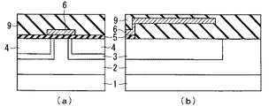
図3〜9は、MOSFET100の製造工程を示す断面図である。以下、図3〜9に沿ってMOSFET100の製造工程を説明する。
熱処理を行うに際して、予めダミー基板22の裏面には無機膜22fを形成したが、表面には無機膜を形成しなくても良い。そうすれば、ダミー基板22の表面を用いて膜厚等のモニターが可能であり、ダミー基板22をモニター基板としても用いることが出来る。この場合、ダミー基板22とは別途のモニター基板を同一バッチ式装置内に設置する必要がないので、処理枚数が増え生産性が向上する。
本発明の半導体装置の製造方法は、(a)ダミー基板22および複数の半導体基板31〜35を準備する工程と、(b)ダミー基板22の裏面と複数の製品基板31〜35(半導体基板)の裏面に、熱酸化処理または熱処理の温度に耐え、酸化または還元ガス種の複数の半導体基板の裏面に到達する量が十分少なくなる膜厚を有する無機膜22f、31f〜35fを形成する工程と、(c)ダミー基板22と複数の製品基板31〜35を表面を同方向に向け互いに間隔を空けて積層するように配置する工程と、(d)工程(b)および(c)の後、酸化ガス雰囲気又は還元ガス雰囲気内で半導体基板31〜35表面の熱酸化処理又はポストアニールを行う工程と、を備える。ダミー基板22および製品基板31〜35夫々の裏面に無機膜を形成することで、加熱処理時の雰囲気ガスが各基板22,31〜35の裏面で消費されないので、製品基板31〜35の表面における雰囲気ガスの消費量が均一になり、電気的特性が均一になる。
Claims (6)
- (a)ダミー基板および、表面を(0001)面とし裏面を(000−1)面とする複数のSiC半導体基板を準備する工程と、
(b)前記ダミー基板の裏面と前記複数のSiC半導体基板の裏面に、無機膜を形成する工程と、
(c)前記ダミー基板と前記複数のSiC半導体基板を表面を同方向に向け互いに間隔を空けて積層するように配置する工程と、
(d)前記工程(b)および(c)の後、酸化ガス雰囲気又は還元ガス雰囲気内で前記SiC半導体基板表面の熱酸化処理又はポストアニールを行う工程と、
を備える半導体装置の製造方法。 - 前記工程(b)は、前記無機膜として、熱酸化膜、CVD酸化膜、金属酸化膜、若しくはPSGのいずれかの絶縁膜、又は窒化膜を形成する工程である、
請求項1に記載の半導体装置の製造方法。 - 前記ダミー基板は前記SiC半導体基板と異なる材料の基板である、
請求項1又は2に記載の半導体装置の製造方法。 - 前記ダミー基板は前記SiC半導体基板と同一材料の基板であり、
前記SiC半導体基板の裏面に前記無機膜が形成されない状態において、前記SiC半導体基板の表面と裏面では熱酸化速度が異なる、
請求項1又は2に記載の半導体装置の製造方法。 - 前記工程(a)は、前記ダミー基板の裏面にのみ前記無機膜を形成する工程である、
請求項1〜4のいずれかに記載の半導体装置の製造方法。 - 前記工程(a)は、石英ガラスからなる前記ダミー基板を準備する工程であり、
前記工程(b)に代えて、
(e)前記複数のSiC半導体基板の裏面に、無機膜を形成する工程を備える、
請求項1〜5のいずれかに記載の半導体装置の製造方法。
Priority Applications (5)
| Application Number | Priority Date | Filing Date | Title |
|---|---|---|---|
| JP2013035300A JP5955246B2 (ja) | 2013-02-26 | 2013-02-26 | 半導体装置の製造方法 |
| US14/071,406 US9159585B2 (en) | 2013-02-26 | 2013-11-04 | Method of manufacturing semiconductor device |
| DE102013225320.6A DE102013225320B4 (de) | 2013-02-26 | 2013-12-09 | Verfahren zum Herstellen einer Halbleitervorrichtung |
| KR1020140015775A KR101597602B1 (ko) | 2013-02-26 | 2014-02-12 | 반도체장치의 제조방법 |
| CN201410067436.2A CN104008969B (zh) | 2013-02-26 | 2014-02-26 | 半导体装置的制造方法 |
Applications Claiming Priority (1)
| Application Number | Priority Date | Filing Date | Title |
|---|---|---|---|
| JP2013035300A JP5955246B2 (ja) | 2013-02-26 | 2013-02-26 | 半導体装置の製造方法 |
Publications (2)
| Publication Number | Publication Date |
|---|---|
| JP2014165348A JP2014165348A (ja) | 2014-09-08 |
| JP5955246B2 true JP5955246B2 (ja) | 2016-07-20 |
Family
ID=51349534
Family Applications (1)
| Application Number | Title | Priority Date | Filing Date |
|---|---|---|---|
| JP2013035300A Active JP5955246B2 (ja) | 2013-02-26 | 2013-02-26 | 半導体装置の製造方法 |
Country Status (5)
| Country | Link |
|---|---|
| US (1) | US9159585B2 (ja) |
| JP (1) | JP5955246B2 (ja) |
| KR (1) | KR101597602B1 (ja) |
| CN (1) | CN104008969B (ja) |
| DE (1) | DE102013225320B4 (ja) |
Families Citing this family (12)
| Publication number | Priority date | Publication date | Assignee | Title |
|---|---|---|---|---|
| DE102014117780B4 (de) * | 2014-12-03 | 2018-06-21 | Infineon Technologies Ag | Halbleiterbauelement mit einer Grabenelektrode und Verfahren zur Herstellung |
| DE102014119465B3 (de) | 2014-12-22 | 2016-05-25 | Infineon Technologies Ag | Halbleitervorrichtung mit streifenförmigen trenchgatestrukturen, transistormesas und diodenmesas |
| JP7154772B2 (ja) * | 2018-02-16 | 2022-10-18 | 株式会社豊田中央研究所 | 炭化珪素半導体装置の製造方法 |
| DE102018103973B4 (de) | 2018-02-22 | 2020-12-03 | Infineon Technologies Ag | Siliziumcarbid-halbleiterbauelement |
| DE102019111308A1 (de) | 2018-05-07 | 2019-11-07 | Infineon Technologies Ag | Siliziumcarbid halbleiterbauelement |
| DE102018124740B4 (de) | 2018-10-08 | 2025-08-28 | Infineon Technologies Ag | Verfahren zur herstellung eines halbleiterbauelements |
| US10586845B1 (en) | 2018-11-16 | 2020-03-10 | Infineon Technologies Ag | SiC trench transistor device and methods of manufacturing thereof |
| US10903322B2 (en) | 2018-11-16 | 2021-01-26 | Infineon Technologies Ag | SiC power semiconductor device with integrated body diode |
| US10985248B2 (en) | 2018-11-16 | 2021-04-20 | Infineon Technologies Ag | SiC power semiconductor device with integrated Schottky junction |
| JP7236947B2 (ja) * | 2019-07-11 | 2023-03-10 | 三菱電機株式会社 | SiC半導体装置の製造方法 |
| JP7563844B2 (ja) * | 2020-11-06 | 2024-10-08 | 東京エレクトロン株式会社 | 熱処理装置及びダミー基板の処理方法 |
| JP7565885B2 (ja) | 2021-07-27 | 2024-10-11 | 三菱電機株式会社 | 半導体装置の製造方法および半導体製造装置 |
Family Cites Families (16)
| Publication number | Priority date | Publication date | Assignee | Title |
|---|---|---|---|---|
| JPS586136A (ja) * | 1981-07-02 | 1983-01-13 | Nec Corp | 半導体ウエ−ハの熱処理法 |
| JPH03224228A (ja) * | 1990-01-30 | 1991-10-03 | Fujitsu Ltd | 半導体装置の製造方法 |
| JPH0799157A (ja) * | 1993-09-29 | 1995-04-11 | Hitachi Ltd | 成膜方法および装置 |
| JPH07254591A (ja) | 1994-03-16 | 1995-10-03 | Toshiba Corp | 熱処理装置 |
| JP2000260718A (ja) * | 1999-03-10 | 2000-09-22 | Sony Corp | ポリシリコンcvd膜の成膜方法 |
| TW538499B (en) * | 2002-06-10 | 2003-06-21 | Taiwan Semiconductor Mfg | Boat with constant backside emissivity to wafers |
| US7667301B2 (en) | 2002-09-27 | 2010-02-23 | Hitachi Kokusai Electric Inc. | Thermal treatment apparatus, method for manufacturing semiconductor device, and method for manufacturing substrate |
| JP2004152920A (ja) | 2002-10-30 | 2004-05-27 | Fujitsu Ltd | 半導体装置の製造方法及び半導体製造工程の管理方法 |
| TWI264758B (en) * | 2004-03-11 | 2006-10-21 | Hitachi Int Electric Inc | A substrate processing apparatus and a semiconductor device manufacturing method use the same |
| US7972703B2 (en) | 2005-03-03 | 2011-07-05 | Ferrotec (Usa) Corporation | Baffle wafers and randomly oriented polycrystalline silicon used therefor |
| JP2008300643A (ja) * | 2007-05-31 | 2008-12-11 | Fujitsu Microelectronics Ltd | 半導体装置の製造方法 |
| JP5246843B2 (ja) | 2007-11-07 | 2013-07-24 | 株式会社日立国際電気 | 基板処理装置、ベーキング方法及び半導体装置の製造方法 |
| JP5239697B2 (ja) * | 2008-09-29 | 2013-07-17 | セイコーエプソン株式会社 | 半導体装置の製造方法、熱酸化処理方法及び熱酸化処理装置 |
| JP2010147265A (ja) * | 2008-12-19 | 2010-07-01 | Hitachi Kokusai Electric Inc | 半導体装置の製造方法 |
| US20120252225A1 (en) * | 2011-03-29 | 2012-10-04 | Chunlong Li | Semiconductor fabrication method |
| CN102723272B (zh) * | 2011-03-29 | 2015-02-25 | 中国科学院微电子研究所 | 半导体制造方法 |
-
2013
- 2013-02-26 JP JP2013035300A patent/JP5955246B2/ja active Active
- 2013-11-04 US US14/071,406 patent/US9159585B2/en active Active
- 2013-12-09 DE DE102013225320.6A patent/DE102013225320B4/de active Active
-
2014
- 2014-02-12 KR KR1020140015775A patent/KR101597602B1/ko not_active Expired - Fee Related
- 2014-02-26 CN CN201410067436.2A patent/CN104008969B/zh active Active
Also Published As
| Publication number | Publication date |
|---|---|
| DE102013225320A1 (de) | 2014-08-28 |
| US20140242815A1 (en) | 2014-08-28 |
| CN104008969A (zh) | 2014-08-27 |
| US9159585B2 (en) | 2015-10-13 |
| KR20140106402A (ko) | 2014-09-03 |
| CN104008969B (zh) | 2017-06-16 |
| DE102013225320B4 (de) | 2019-06-19 |
| JP2014165348A (ja) | 2014-09-08 |
| KR101597602B1 (ko) | 2016-02-25 |
Similar Documents
| Publication | Publication Date | Title |
|---|---|---|
| JP2014165348A (ja) | 半導体装置の製造方法 | |
| JP6120756B2 (ja) | 炭化珪素半導体装置とその製造方法 | |
| US20120007104A1 (en) | Semiconductor device and method for manufacturing same | |
| JP6918302B2 (ja) | 炭化珪素半導体装置および炭化珪素半導体装置の製造方法 | |
| JP5889171B2 (ja) | 炭化珪素半導体装置及びその製造方法 | |
| JPWO2010125661A1 (ja) | 半導体装置及びその製造方法 | |
| JP2012160485A (ja) | 半導体装置とその製造方法 | |
| US9613809B2 (en) | Method of manufacturing silicon carbide semiconductor device | |
| JP2024001352A (ja) | 半導体装置の製造方法 | |
| US20130292703A1 (en) | Semiconductor device and method for manufacturing same | |
| JP2015103631A (ja) | 炭化珪素半導体装置および炭化珪素半導体装置の製造方法 | |
| JPWO2016013471A1 (ja) | 半導体装置及び半導体装置の製造方法 | |
| JP6208106B2 (ja) | 半導体装置及びその製造方法 | |
| JP2014127660A (ja) | 炭化珪素ダイオード、炭化珪素トランジスタおよび炭化珪素半導体装置の製造方法 | |
| CN102132388A (zh) | 双极型半导体装置及其制造方法 | |
| CN104282766A (zh) | 一种新型碳化硅mosfet及其制造方法 | |
| CN107204363A (zh) | 碳化硅半导体装置及碳化硅半导体装置的制造方法 | |
| JP5236787B2 (ja) | 窒化物半導体装置およびその製造方法 | |
| JP2015015352A (ja) | 炭化珪素半導体装置の製造方法 | |
| JP5526493B2 (ja) | トレンチゲート型半導体装置およびその製造方法 | |
| JP6690333B2 (ja) | 炭化珪素半導体装置および炭化珪素半導体装置の製造方法 | |
| US20150091021A1 (en) | Method of Manufacturing Semiconductor Device and the Semiconductor Device | |
| JP6441412B2 (ja) | 半導体装置 | |
| JP2017168681A (ja) | 半導体装置および半導体装置の製造方法 | |
| CN104319292A (zh) | 一种新型碳化硅mosfet及其制造方法 |
Legal Events
| Date | Code | Title | Description |
|---|---|---|---|
| A621 | Written request for application examination |
Free format text: JAPANESE INTERMEDIATE CODE: A621 Effective date: 20150430 |
|
| A977 | Report on retrieval |
Free format text: JAPANESE INTERMEDIATE CODE: A971007 Effective date: 20160217 |
|
| A131 | Notification of reasons for refusal |
Free format text: JAPANESE INTERMEDIATE CODE: A131 Effective date: 20160223 |
|
| A521 | Request for written amendment filed |
Free format text: JAPANESE INTERMEDIATE CODE: A523 Effective date: 20160415 |
|
| TRDD | Decision of grant or rejection written | ||
| A01 | Written decision to grant a patent or to grant a registration (utility model) |
Free format text: JAPANESE INTERMEDIATE CODE: A01 Effective date: 20160517 |
|
| A61 | First payment of annual fees (during grant procedure) |
Free format text: JAPANESE INTERMEDIATE CODE: A61 Effective date: 20160614 |
|
| R150 | Certificate of patent or registration of utility model |
Ref document number: 5955246 Country of ref document: JP Free format text: JAPANESE INTERMEDIATE CODE: R150 |
|
| R250 | Receipt of annual fees |
Free format text: JAPANESE INTERMEDIATE CODE: R250 |
|
| R250 | Receipt of annual fees |
Free format text: JAPANESE INTERMEDIATE CODE: R250 |
|
| R250 | Receipt of annual fees |
Free format text: JAPANESE INTERMEDIATE CODE: R250 |
|
| R250 | Receipt of annual fees |
Free format text: JAPANESE INTERMEDIATE CODE: R250 |
|
| R250 | Receipt of annual fees |
Free format text: JAPANESE INTERMEDIATE CODE: R250 |
|
| R250 | Receipt of annual fees |
Free format text: JAPANESE INTERMEDIATE CODE: R250 |
|
| R250 | Receipt of annual fees |
Free format text: JAPANESE INTERMEDIATE CODE: R250 |