JP6046867B2 - 配線体、配線基板、タッチセンサ、及び配線体の製造方法 - Google Patents
配線体、配線基板、タッチセンサ、及び配線体の製造方法 Download PDFInfo
- Publication number
- JP6046867B2 JP6046867B2 JP2016532147A JP2016532147A JP6046867B2 JP 6046867 B2 JP6046867 B2 JP 6046867B2 JP 2016532147 A JP2016532147 A JP 2016532147A JP 2016532147 A JP2016532147 A JP 2016532147A JP 6046867 B2 JP6046867 B2 JP 6046867B2
- Authority
- JP
- Japan
- Prior art keywords
- wiring body
- conductor pattern
- wiring
- conductive
- side portion
- Prior art date
- Legal status (The legal status is an assumption and is not a legal conclusion. Google has not performed a legal analysis and makes no representation as to the accuracy of the status listed.)
- Expired - Fee Related
Links
Images




Classifications
-
- G—PHYSICS
- G06—COMPUTING OR CALCULATING; COUNTING
- G06F—ELECTRIC DIGITAL DATA PROCESSING
- G06F3/00—Input arrangements for transferring data to be processed into a form capable of being handled by the computer; Output arrangements for transferring data from processing unit to output unit, e.g. interface arrangements
- G06F3/01—Input arrangements or combined input and output arrangements for interaction between user and computer
- G06F3/03—Arrangements for converting the position or the displacement of a member into a coded form
- G06F3/041—Digitisers, e.g. for touch screens or touch pads, characterised by the transducing means
-
- H—ELECTRICITY
- H05—ELECTRIC TECHNIQUES NOT OTHERWISE PROVIDED FOR
- H05K—PRINTED CIRCUITS; CASINGS OR CONSTRUCTIONAL DETAILS OF ELECTRIC APPARATUS; MANUFACTURE OF ASSEMBLAGES OF ELECTRICAL COMPONENTS
- H05K3/00—Apparatus or processes for manufacturing printed circuits
- H05K3/10—Apparatus or processes for manufacturing printed circuits in which conductive material is applied to the insulating support in such a manner as to form the desired conductive pattern
- H05K3/20—Apparatus or processes for manufacturing printed circuits in which conductive material is applied to the insulating support in such a manner as to form the desired conductive pattern by affixing prefabricated conductor pattern
-
- H—ELECTRICITY
- H05—ELECTRIC TECHNIQUES NOT OTHERWISE PROVIDED FOR
- H05K—PRINTED CIRCUITS; CASINGS OR CONSTRUCTIONAL DETAILS OF ELECTRIC APPARATUS; MANUFACTURE OF ASSEMBLAGES OF ELECTRICAL COMPONENTS
- H05K3/00—Apparatus or processes for manufacturing printed circuits
- H05K3/10—Apparatus or processes for manufacturing printed circuits in which conductive material is applied to the insulating support in such a manner as to form the desired conductive pattern
- H05K3/20—Apparatus or processes for manufacturing printed circuits in which conductive material is applied to the insulating support in such a manner as to form the desired conductive pattern by affixing prefabricated conductor pattern
- H05K3/207—Apparatus or processes for manufacturing printed circuits in which conductive material is applied to the insulating support in such a manner as to form the desired conductive pattern by affixing prefabricated conductor pattern using a prefabricated paste pattern, ink pattern or powder pattern
-
- H—ELECTRICITY
- H05—ELECTRIC TECHNIQUES NOT OTHERWISE PROVIDED FOR
- H05K—PRINTED CIRCUITS; CASINGS OR CONSTRUCTIONAL DETAILS OF ELECTRIC APPARATUS; MANUFACTURE OF ASSEMBLAGES OF ELECTRICAL COMPONENTS
- H05K3/00—Apparatus or processes for manufacturing printed circuits
- H05K3/38—Improvement of the adhesion between the insulating substrate and the metal
- H05K3/386—Improvement of the adhesion between the insulating substrate and the metal by the use of an organic polymeric bonding layer, e.g. adhesive
-
- G—PHYSICS
- G06—COMPUTING OR CALCULATING; COUNTING
- G06F—ELECTRIC DIGITAL DATA PROCESSING
- G06F2203/00—Indexing scheme relating to G06F3/00 - G06F3/048
- G06F2203/041—Indexing scheme relating to G06F3/041 - G06F3/045
- G06F2203/04103—Manufacturing, i.e. details related to manufacturing processes specially suited for touch sensitive devices
-
- G—PHYSICS
- G06—COMPUTING OR CALCULATING; COUNTING
- G06F—ELECTRIC DIGITAL DATA PROCESSING
- G06F3/00—Input arrangements for transferring data to be processed into a form capable of being handled by the computer; Output arrangements for transferring data from processing unit to output unit, e.g. interface arrangements
- G06F3/01—Input arrangements or combined input and output arrangements for interaction between user and computer
- G06F3/03—Arrangements for converting the position or the displacement of a member into a coded form
- G06F3/041—Digitisers, e.g. for touch screens or touch pads, characterised by the transducing means
- G06F3/044—Digitisers, e.g. for touch screens or touch pads, characterised by the transducing means by capacitive means
-
- H—ELECTRICITY
- H05—ELECTRIC TECHNIQUES NOT OTHERWISE PROVIDED FOR
- H05K—PRINTED CIRCUITS; CASINGS OR CONSTRUCTIONAL DETAILS OF ELECTRIC APPARATUS; MANUFACTURE OF ASSEMBLAGES OF ELECTRICAL COMPONENTS
- H05K1/00—Printed circuits
- H05K1/02—Details
- H05K1/0274—Optical details, e.g. printed circuits comprising integral optical means
-
- H—ELECTRICITY
- H05—ELECTRIC TECHNIQUES NOT OTHERWISE PROVIDED FOR
- H05K—PRINTED CIRCUITS; CASINGS OR CONSTRUCTIONAL DETAILS OF ELECTRIC APPARATUS; MANUFACTURE OF ASSEMBLAGES OF ELECTRICAL COMPONENTS
- H05K1/00—Printed circuits
- H05K1/02—Details
- H05K1/09—Use of materials for the conductive, e.g. metallic pattern
- H05K1/092—Dispersed materials, e.g. conductive pastes or inks
-
- H—ELECTRICITY
- H05—ELECTRIC TECHNIQUES NOT OTHERWISE PROVIDED FOR
- H05K—PRINTED CIRCUITS; CASINGS OR CONSTRUCTIONAL DETAILS OF ELECTRIC APPARATUS; MANUFACTURE OF ASSEMBLAGES OF ELECTRICAL COMPONENTS
- H05K2201/00—Indexing scheme relating to printed circuits covered by H05K1/00
- H05K2201/01—Dielectrics
- H05K2201/0104—Properties and characteristics in general
- H05K2201/0108—Transparent
-
- H—ELECTRICITY
- H05—ELECTRIC TECHNIQUES NOT OTHERWISE PROVIDED FOR
- H05K—PRINTED CIRCUITS; CASINGS OR CONSTRUCTIONAL DETAILS OF ELECTRIC APPARATUS; MANUFACTURE OF ASSEMBLAGES OF ELECTRICAL COMPONENTS
- H05K2201/00—Indexing scheme relating to printed circuits covered by H05K1/00
- H05K2201/09—Shape and layout
- H05K2201/09209—Shape and layout details of conductors
- H05K2201/09654—Shape and layout details of conductors covering at least two types of conductors provided for in H05K2201/09218 - H05K2201/095
- H05K2201/09681—Mesh conductors, e.g. as a ground plane
-
- H—ELECTRICITY
- H05—ELECTRIC TECHNIQUES NOT OTHERWISE PROVIDED FOR
- H05K—PRINTED CIRCUITS; CASINGS OR CONSTRUCTIONAL DETAILS OF ELECTRIC APPARATUS; MANUFACTURE OF ASSEMBLAGES OF ELECTRICAL COMPONENTS
- H05K2201/00—Indexing scheme relating to printed circuits covered by H05K1/00
- H05K2201/09—Shape and layout
- H05K2201/09818—Shape or layout details not covered by a single group of H05K2201/09009 - H05K2201/09809
- H05K2201/09827—Tapered, e.g. tapered hole, via or groove
-
- H—ELECTRICITY
- H05—ELECTRIC TECHNIQUES NOT OTHERWISE PROVIDED FOR
- H05K—PRINTED CIRCUITS; CASINGS OR CONSTRUCTIONAL DETAILS OF ELECTRIC APPARATUS; MANUFACTURE OF ASSEMBLAGES OF ELECTRICAL COMPONENTS
- H05K2203/00—Indexing scheme relating to apparatus or processes for manufacturing printed circuits covered by H05K3/00
- H05K2203/01—Tools for processing; Objects used during processing
- H05K2203/0104—Tools for processing; Objects used during processing for patterning or coating
- H05K2203/0113—Female die used for patterning or transferring, e.g. temporary substrate having recessed pattern
-
- H—ELECTRICITY
- H05—ELECTRIC TECHNIQUES NOT OTHERWISE PROVIDED FOR
- H05K—PRINTED CIRCUITS; CASINGS OR CONSTRUCTIONAL DETAILS OF ELECTRIC APPARATUS; MANUFACTURE OF ASSEMBLAGES OF ELECTRICAL COMPONENTS
- H05K2203/00—Indexing scheme relating to apparatus or processes for manufacturing printed circuits covered by H05K3/00
- H05K2203/05—Patterning and lithography; Masks; Details of resist
- H05K2203/0502—Patterning and lithography
-
- H—ELECTRICITY
- H05—ELECTRIC TECHNIQUES NOT OTHERWISE PROVIDED FOR
- H05K—PRINTED CIRCUITS; CASINGS OR CONSTRUCTIONAL DETAILS OF ELECTRIC APPARATUS; MANUFACTURE OF ASSEMBLAGES OF ELECTRICAL COMPONENTS
- H05K3/00—Apparatus or processes for manufacturing printed circuits
- H05K3/10—Apparatus or processes for manufacturing printed circuits in which conductive material is applied to the insulating support in such a manner as to form the desired conductive pattern
- H05K3/12—Apparatus or processes for manufacturing printed circuits in which conductive material is applied to the insulating support in such a manner as to form the desired conductive pattern using thick film techniques, e.g. printing techniques to apply the conductive material or similar techniques for applying conductive paste or ink patterns
- H05K3/1275—Apparatus or processes for manufacturing printed circuits in which conductive material is applied to the insulating support in such a manner as to form the desired conductive pattern using thick film techniques, e.g. printing techniques to apply the conductive material or similar techniques for applying conductive paste or ink patterns by other printing techniques, e.g. letterpress printing, intaglio printing, lithographic printing, offset printing
Landscapes
- Engineering & Computer Science (AREA)
- Manufacturing & Machinery (AREA)
- Microelectronics & Electronic Packaging (AREA)
- General Engineering & Computer Science (AREA)
- Theoretical Computer Science (AREA)
- Human Computer Interaction (AREA)
- Physics & Mathematics (AREA)
- General Physics & Mathematics (AREA)
- Manufacturing Of Printed Wiring (AREA)
- Structure Of Printed Boards (AREA)
Description
文献の参照による組み込みが認められる指定国については、2014年12月26日に日本国に出願された特願2014−264492号に記載された内容を参照により本明細書に組み込み、本明細書の記載の一部とする。
[2]上記発明において、前記導電性粒子の平均粒径は、0.5μm〜2μmであってもよい。
[3]上記発明において、前記導体パターンの接着面の面粗さは、0.1μm〜3μmであってもよい。
0.5≦B/A・・・(1)
但し、上記(1)式において、Aは前記導体パターンの断面視における最大幅であり、Bは前記導体パターンの前記断面視における最大高さである。
前記頂辺部は、平坦部を含んでもよい。
0.5≦D/C・・・(2)
但し、上記(2)式において、Cは乾燥、加熱及びエネルギー線の照射のうちの少なくとも1つが行われた前記導電性材料の断面視における最大幅であり、Dは加熱又はエネルギー線を照射された前記導電性材料の前記断面視における最大高さである。
0.5≦B/A・・・(3)
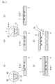
但し、上記(3)式において、Aは導体パターン41の断面視における最大幅であり、Bは導体パターン41の当該断面視における最大高さ(厚さ)である。なお、上記(3)式のB/Aは、3以下(B/A≦3)であることが好ましい。
0.5≦D/C・・・(4)
但し、上記(4)式において、Cは加熱された導電性材料6の断面視における最大幅であり、Dは加熱された導電性材料6の当該断面視における最大高さ(厚さ)である(図4(Bの引き出し図参照)。なお、上記(4)式のD/Cは、3以下(D/C≦3)であることが好ましい。
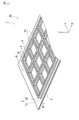
1、1B・・・配線体
2・・・基材
3・・・接着層
31・・・支持部
32・・・平状部
4・・・導伝層
41・・・導体パターン
42・・・下面(接着面)
43・・・頂辺部
431・・・平坦部
44・・・側部
44a,44b・・・第1及び第2の部分
441・・・平坦部
45・・・第2の側部
46・・・曲面
47・・・上面
5・・・凹版
51・・・凹部
52・・・内壁
53・・・底面
6・・・導電性材料
7、7B・・・接着性材料
Claims (15)
- 絶縁部材と、
導電性粒子及びバインダ樹脂を含み、前記絶縁部材に接着される導体パターンと、を備え、
前記導体パターンにおいて前記絶縁部材に接着される接着面において、前記導電性粒子の一部が前記バインダ樹脂から突出しており、
前記導体パターンの接着面の面粗さは、前記導体パターンにおいて前記接着面を除く他の面の面粗さよりも粗く、
前記絶縁部材と前記導体パターンとの境界は、前記導体パターンの接着面の面粗さに基づいた凹凸形状に対応した凹凸形状となっていることを特徴とする配線体。 - 請求項1に記載の配線体であって、
前記導電性粒子の平均粒径は、0.5μm〜2μmであることを特徴とする配線体。 - 請求項1又は2に記載の配線体であって、
前記導体パターンの接着面の面粗さは、0.1μm〜3μmであることを特徴とする配線体。 - 請求項1〜3の何れか1項に記載の配線体であって、
下記(1)式を満たすことを特徴とする配線体。
0.5≦B/A・・・(1)
但し、上記(1)式において、Aは前記導体パターンの断面視における最大幅であり、Bは前記導体パターンの前記断面視における最大高さである。 - 請求項1〜4の何れか1項に記載の配線体であって、
前記他の面は、前記接着面の反対側に位置する頂辺部を有し、
前記頂辺部は、平坦部を含むことを特徴とする配線体。 - 請求項1〜5の何れか1項に記載の配線体であって、
前記他の面は、
前記接着面の反対側に位置する頂辺部と、
前記接着面と前記頂辺部との間に位置する側部を有し、
前記側部は、断面視において、前記絶縁部材から離れる方向に従い、前記導体パターンの中心に接近するように傾斜していることを特徴とする配線体。 - 請求項6に記載の配線体であって、
前記頂辺部と前記側部との間の角度θは、90°〜120°であることを特徴とする配線体。 - 請求項6又は7に記載の配線体であって、
前記側部は、断面視において、
前記頂辺部と繋がる第1の部分と、
前記第1の部分よりも外側に位置し、前記接着面と繋がる第2の部分と、を有しており、
前記側部は、断面視において、前記第1及び第2の部分を通る仮想直線と実質的に一致している、又は、前記仮想直線よりも外側に突出していることを特徴とする配線体。 - 請求項1〜8の何れか1項に記載の配線体であって、
前記導電性粒子の平均直径は、前記導体パターンの幅の半分以下であることを特徴とする配線体。 - 請求項1〜9の何れか1項に記載の配線体であって、
前記導体パターンの幅は、1μm〜5μmであることを特徴とする配線体。 - 請求項1〜10のいずれか一項に記載の配線体であって、
前記他の面側における前記配線体の乱反射率は、前記接着面側における前記配線体の乱反射率に対して相対的に小さいことを特徴とする配線体。 - 請求項1〜11の何れか1項に記載の配線体と、
前記配線体を支持する支持体と、を備えることを特徴とする配線基板。 - 請求項12に記載の配線基板を備えることを特徴とするタッチセンサ。
- 凹版の凹部に導電性粒子及びバインダ樹脂を含む導電性材料を充填する第1の工程と、
前記凹版に充填された前記導電性材料に対して乾燥、加熱及びエネルギー線の照射のうちの少なくとも1つを行い、前記導電性材料の上面に、前記導電性粒子の一部が前記バインダ樹脂から突出した凹凸形状を形成し、前記導電性材料から導体パターンを形成する第2の工程と、
前記凹凸形状に絶縁材を入り込ませる第3の工程と、
少なくとも前記絶縁材及び前記導体パターンを、前記凹版から離型する第4の工程と、を備えたことを特徴とする配線体の製造方法。 - 請求項14に記載の配線体の製造方法であって、
前記第3の工程は、前記凹凸形状に入り込んだ前記絶縁材の上に基材を配置する工程を含み、
前記第4の工程は、前記導体パターンが前記絶縁材を介して前記基材に固定された状態で、前記基材、前記絶縁材及び前記導体パターンを、前記凹版から離型する工程であることを特徴とする配線体の製造方法。
Applications Claiming Priority (3)
| Application Number | Priority Date | Filing Date | Title |
|---|---|---|---|
| JP2014264492 | 2014-12-26 | ||
| JP2014264492 | 2014-12-26 | ||
| PCT/JP2015/086271 WO2016104723A1 (ja) | 2014-12-26 | 2015-12-25 | 配線体、配線基板、タッチセンサ、及び配線体の製造方法 |
Related Child Applications (1)
| Application Number | Title | Priority Date | Filing Date |
|---|---|---|---|
| JP2016223848A Division JP6735212B2 (ja) | 2014-12-26 | 2016-11-17 | 配線体、配線基板、タッチセンサ、及び配線体の製造方法 |
Publications (2)
| Publication Number | Publication Date |
|---|---|
| JP6046867B2 true JP6046867B2 (ja) | 2016-12-21 |
| JPWO2016104723A1 JPWO2016104723A1 (ja) | 2017-04-27 |
Family
ID=56150735
Family Applications (2)
| Application Number | Title | Priority Date | Filing Date |
|---|---|---|---|
| JP2016532147A Expired - Fee Related JP6046867B2 (ja) | 2014-12-26 | 2015-12-25 | 配線体、配線基板、タッチセンサ、及び配線体の製造方法 |
| JP2016223848A Expired - Fee Related JP6735212B2 (ja) | 2014-12-26 | 2016-11-17 | 配線体、配線基板、タッチセンサ、及び配線体の製造方法 |
Family Applications After (1)
| Application Number | Title | Priority Date | Filing Date |
|---|---|---|---|
| JP2016223848A Expired - Fee Related JP6735212B2 (ja) | 2014-12-26 | 2016-11-17 | 配線体、配線基板、タッチセンサ、及び配線体の製造方法 |
Country Status (6)
| Country | Link |
|---|---|
| US (1) | US10379645B2 (ja) |
| EP (1) | EP3190488B1 (ja) |
| JP (2) | JP6046867B2 (ja) |
| CN (1) | CN106687893B (ja) |
| TW (1) | TWI587191B (ja) |
| WO (1) | WO2016104723A1 (ja) |
Cited By (1)
| Publication number | Priority date | Publication date | Assignee | Title |
|---|---|---|---|---|
| KR20190121014A (ko) * | 2018-04-17 | 2019-10-25 | 울산과학기술원 | 자가 부착 투명 전극 및 이의 제조방법 |
Families Citing this family (13)
| Publication number | Priority date | Publication date | Assignee | Title |
|---|---|---|---|---|
| EP3177117A4 (en) * | 2015-01-30 | 2017-12-20 | Fujikura, Ltd. | Wiring body, wiring substrate, and touch sensor |
| CN104820533B (zh) * | 2015-05-22 | 2019-03-12 | 京东方科技集团股份有限公司 | 触摸基板及其制备方法、显示装置 |
| CN107124900A (zh) * | 2015-12-25 | 2017-09-01 | 松下知识产权经营株式会社 | 触摸面板和使用该触摸面板的显示装置 |
| US20190327829A1 (en) * | 2016-07-12 | 2019-10-24 | Fujikura Ltd. | Stretchable board |
| US12446160B2 (en) * | 2016-07-28 | 2025-10-14 | Landa Labs (2012) Ltd. | Application of electrical conductors to an electrically insulating substrate |
| GB201613051D0 (en) * | 2016-07-28 | 2016-09-14 | Landa Labs (2012) Ltd | Applying an electrical conductor to a substrate |
| JP2019046405A (ja) * | 2017-09-07 | 2019-03-22 | 日本航空電子工業株式会社 | タッチセンサデバイス |
| CN112771722B (zh) * | 2018-09-28 | 2024-06-25 | 大日本印刷株式会社 | 配线基板和配线基板的制造方法 |
| JP7115687B2 (ja) | 2019-01-23 | 2022-08-09 | 株式会社デンソー | カーボンナノチューブパターン配線、それを有する透明導電基板およびヒータ |
| KR102705615B1 (ko) * | 2019-06-25 | 2024-09-12 | 삼성디스플레이 주식회사 | 표시 장치의 제조 방법 및 이에 사용되는 레이저 장치 |
| JP7667960B2 (ja) * | 2020-05-01 | 2025-04-24 | 大日本印刷株式会社 | 配線基板及び配線基板の製造方法 |
| JP7374059B2 (ja) * | 2020-09-25 | 2023-11-06 | コネクテックジャパン株式会社 | 配線形成方法 |
| TWI784681B (zh) | 2021-08-20 | 2022-11-21 | 錼創顯示科技股份有限公司 | 微型發光二極體顯示裝置 |
Citations (9)
| Publication number | Priority date | Publication date | Assignee | Title |
|---|---|---|---|---|
| JPH04240792A (ja) * | 1991-01-24 | 1992-08-28 | Matsushita Electric Ind Co Ltd | 回路基板の製造方法 |
| JPH07169635A (ja) * | 1993-09-21 | 1995-07-04 | Matsushita Electric Ind Co Ltd | 電子部品およびその製造方法 |
| JP2006302930A (ja) * | 2005-04-15 | 2006-11-02 | Matsushita Electric Ind Co Ltd | 配線基板とそれを用いた電子部品実装体およびそれらの製造方法 |
| JP2008139730A (ja) * | 2006-12-05 | 2008-06-19 | Nippon Oil Corp | ワイヤグリッド型偏光子及びその製造方法、並びにそれを用いた位相差フィルム及び液晶表示素子 |
| WO2008149969A1 (ja) * | 2007-06-08 | 2008-12-11 | Dai Nippon Printing Co., Ltd. | 印刷物及びその製造方法並びに電磁波シールド材及びその製造方法 |
| JP2011139097A (ja) * | 2005-04-25 | 2011-07-14 | Brother Industries Ltd | パターン形成方法 |
| JP2012168301A (ja) * | 2011-02-14 | 2012-09-06 | Bridgestone Corp | 金属細線の形成方法及びこれを用いたワイヤグリッド型偏光子の製造方法 |
| JP2012185813A (ja) * | 2011-02-18 | 2012-09-27 | Fujifilm Corp | 導電シート及びタッチパネル |
| JP2013207038A (ja) * | 2012-03-28 | 2013-10-07 | Dainippon Printing Co Ltd | 透視性電極部材、及び画像表示装置 |
Family Cites Families (18)
| Publication number | Priority date | Publication date | Assignee | Title |
|---|---|---|---|---|
| US5201268A (en) | 1990-12-25 | 1993-04-13 | Matsushita Electric Industrial Co., Ltd. | Intaglio printing process and its application |
| US5609704A (en) | 1993-09-21 | 1997-03-11 | Matsushita Electric Industrial Co., Ltd. | Method for fabricating an electronic part by intaglio printing |
| WO2005069713A1 (ja) * | 2004-01-13 | 2005-07-28 | Dai Nippon Printing Co., Ltd. | 電磁波シールドシート及びその製造方法 |
| US8033016B2 (en) | 2005-04-15 | 2011-10-11 | Panasonic Corporation | Method for manufacturing an electrode and electrode component mounted body |
| TW200738913A (en) | 2006-03-10 | 2007-10-16 | Mitsui Mining & Smelting Co | Surface treated elctrolytic copper foil and process for producing the same |
| JP2007324426A (ja) * | 2006-06-02 | 2007-12-13 | Hitachi Ltd | パターン形成方法、導体配線パターン |
| KR100782412B1 (ko) | 2006-10-25 | 2007-12-05 | 삼성전기주식회사 | 전사회로 형성방법 및 회로기판 제조방법 |
| CN103465525B (zh) * | 2006-12-27 | 2015-10-21 | 日立化成株式会社 | 凹版和使用该凹版的带有导体层图形的基材 |
| JP2010109012A (ja) * | 2008-10-28 | 2010-05-13 | Dainippon Printing Co Ltd | フィルタ、及びその製造方法 |
| KR20110103835A (ko) * | 2008-12-02 | 2011-09-21 | 다이니폰 인사츠 가부시키가이샤 | 전자기파 차폐재, 및 그 제조 방법 |
| TWI467214B (zh) * | 2009-09-02 | 2015-01-01 | Dexerials Corp | A conductive optical element, a touch panel, an information input device, a display device, a solar cell, and a conductive optical element |
| JP5516077B2 (ja) * | 2009-09-30 | 2014-06-11 | 大日本印刷株式会社 | タッチパネル用電極フィルム及びタッチパネル |
| JP5404468B2 (ja) | 2010-02-22 | 2014-01-29 | 京セラ株式会社 | 回路基板 |
| JP2012033466A (ja) * | 2010-07-02 | 2012-02-16 | Fujifilm Corp | 導電層転写材料、及びタッチパネル |
| JP2012155369A (ja) | 2011-01-21 | 2012-08-16 | Japan Aviation Electronics Industry Ltd | 静電容量式タッチパネル |
| JP2014021401A (ja) * | 2012-07-20 | 2014-02-03 | Dexerials Corp | 導電性光学素子、入力素子、および表示素子 |
| JP5922008B2 (ja) | 2012-11-30 | 2016-05-24 | 富士フイルム株式会社 | 転写フィルムおよび透明積層体、それらの製造方法、静電容量型入力装置ならびに画像表示装置 |
| JP5704200B2 (ja) | 2013-08-21 | 2015-04-22 | 大日本印刷株式会社 | タッチパネル用電極フィルム及びタッチパネル |
-
2015
- 2015-12-25 JP JP2016532147A patent/JP6046867B2/ja not_active Expired - Fee Related
- 2015-12-25 WO PCT/JP2015/086271 patent/WO2016104723A1/ja not_active Ceased
- 2015-12-25 CN CN201580047455.1A patent/CN106687893B/zh not_active Expired - Fee Related
- 2015-12-25 EP EP15873291.7A patent/EP3190488B1/en not_active Not-in-force
- 2015-12-25 US US15/508,310 patent/US10379645B2/en active Active
- 2015-12-25 TW TW104143738A patent/TWI587191B/zh not_active IP Right Cessation
-
2016
- 2016-11-17 JP JP2016223848A patent/JP6735212B2/ja not_active Expired - Fee Related
Patent Citations (9)
| Publication number | Priority date | Publication date | Assignee | Title |
|---|---|---|---|---|
| JPH04240792A (ja) * | 1991-01-24 | 1992-08-28 | Matsushita Electric Ind Co Ltd | 回路基板の製造方法 |
| JPH07169635A (ja) * | 1993-09-21 | 1995-07-04 | Matsushita Electric Ind Co Ltd | 電子部品およびその製造方法 |
| JP2006302930A (ja) * | 2005-04-15 | 2006-11-02 | Matsushita Electric Ind Co Ltd | 配線基板とそれを用いた電子部品実装体およびそれらの製造方法 |
| JP2011139097A (ja) * | 2005-04-25 | 2011-07-14 | Brother Industries Ltd | パターン形成方法 |
| JP2008139730A (ja) * | 2006-12-05 | 2008-06-19 | Nippon Oil Corp | ワイヤグリッド型偏光子及びその製造方法、並びにそれを用いた位相差フィルム及び液晶表示素子 |
| WO2008149969A1 (ja) * | 2007-06-08 | 2008-12-11 | Dai Nippon Printing Co., Ltd. | 印刷物及びその製造方法並びに電磁波シールド材及びその製造方法 |
| JP2012168301A (ja) * | 2011-02-14 | 2012-09-06 | Bridgestone Corp | 金属細線の形成方法及びこれを用いたワイヤグリッド型偏光子の製造方法 |
| JP2012185813A (ja) * | 2011-02-18 | 2012-09-27 | Fujifilm Corp | 導電シート及びタッチパネル |
| JP2013207038A (ja) * | 2012-03-28 | 2013-10-07 | Dainippon Printing Co Ltd | 透視性電極部材、及び画像表示装置 |
Cited By (2)
| Publication number | Priority date | Publication date | Assignee | Title |
|---|---|---|---|---|
| KR20190121014A (ko) * | 2018-04-17 | 2019-10-25 | 울산과학기술원 | 자가 부착 투명 전극 및 이의 제조방법 |
| KR102083184B1 (ko) | 2018-04-17 | 2020-03-02 | 울산과학기술원 | 자가 부착 투명 전극 및 이의 제조방법 |
Also Published As
| Publication number | Publication date |
|---|---|
| JP2017041654A (ja) | 2017-02-23 |
| CN106687893B (zh) | 2020-05-22 |
| TWI587191B (zh) | 2017-06-11 |
| US10379645B2 (en) | 2019-08-13 |
| TW201636797A (zh) | 2016-10-16 |
| CN106687893A (zh) | 2017-05-17 |
| JP6735212B2 (ja) | 2020-08-05 |
| WO2016104723A1 (ja) | 2016-06-30 |
| EP3190488A4 (en) | 2017-10-25 |
| JPWO2016104723A1 (ja) | 2017-04-27 |
| EP3190488A1 (en) | 2017-07-12 |
| EP3190488B1 (en) | 2019-05-15 |
| US20170285786A1 (en) | 2017-10-05 |
Similar Documents
| Publication | Publication Date | Title |
|---|---|---|
| JP6046867B2 (ja) | 配線体、配線基板、タッチセンサ、及び配線体の製造方法 | |
| JP6027296B1 (ja) | 配線体、配線基板、及びタッチセンサ | |
| JP6159904B2 (ja) | 配線体、配線基板、及びタッチセンサ | |
| JP6140383B2 (ja) | 導体層付き構造体の製造方法、基材付き配線体、基材付き構造体、及びタッチセンサ | |
| JPWO2017187266A1 (ja) | 配線体、配線体アセンブリ、配線基板、及びタッチセンサ | |
| JP6483801B2 (ja) | タッチセンサ | |
| CN107407997A (zh) | 触摸传感器用配线体、触摸传感器用配线基板以及触摸传感器 | |
| US9910552B2 (en) | Wiring body, wiring board, touch sensor, and method for producing wiring body | |
| JPWO2017069156A1 (ja) | 配線体、配線基板、タッチセンサ、及び配線体の製造方法 | |
| JP6577662B2 (ja) | 配線体、配線基板、及びタッチセンサ | |
| JPWO2017154941A1 (ja) | 配線体、配線基板、及びタッチセンサ | |
| JP6143909B1 (ja) | 配線体、配線基板、タッチセンサ、及び配線体の製造方法 | |
| JP6062135B1 (ja) | 配線体、配線基板、配線構造体、及びタッチセンサ |
Legal Events
| Date | Code | Title | Description |
|---|---|---|---|
| A521 | Request for written amendment filed |
Free format text: JAPANESE INTERMEDIATE CODE: A523 Effective date: 20160518 |
|
| A621 | Written request for application examination |
Free format text: JAPANESE INTERMEDIATE CODE: A621 Effective date: 20160518 |
|
| A871 | Explanation of circumstances concerning accelerated examination |
Free format text: JAPANESE INTERMEDIATE CODE: A871 Effective date: 20160518 |
|
| A975 | Report on accelerated examination |
Free format text: JAPANESE INTERMEDIATE CODE: A971005 Effective date: 20160704 |
|
| A131 | Notification of reasons for refusal |
Free format text: JAPANESE INTERMEDIATE CODE: A131 Effective date: 20160712 |
|
| A521 | Request for written amendment filed |
Free format text: JAPANESE INTERMEDIATE CODE: A523 Effective date: 20160909 |
|
| A521 | Request for written amendment filed |
Free format text: JAPANESE INTERMEDIATE CODE: A821 Effective date: 20160912 |
|
| TRDD | Decision of grant or rejection written | ||
| A01 | Written decision to grant a patent or to grant a registration (utility model) |
Free format text: JAPANESE INTERMEDIATE CODE: A01 Effective date: 20161018 |
|
| A61 | First payment of annual fees (during grant procedure) |
Free format text: JAPANESE INTERMEDIATE CODE: A61 Effective date: 20161117 |
|
| R151 | Written notification of patent or utility model registration |
Ref document number: 6046867 Country of ref document: JP Free format text: JAPANESE INTERMEDIATE CODE: R151 |
|
| R250 | Receipt of annual fees |
Free format text: JAPANESE INTERMEDIATE CODE: R250 |
|
| R250 | Receipt of annual fees |
Free format text: JAPANESE INTERMEDIATE CODE: R250 |
|
| R250 | Receipt of annual fees |
Free format text: JAPANESE INTERMEDIATE CODE: R250 |
|
| R250 | Receipt of annual fees |
Free format text: JAPANESE INTERMEDIATE CODE: R250 |
|
| LAPS | Cancellation because of no payment of annual fees |