JP6049111B2 - Organic thin film transistor array substrate, method for manufacturing the same, and display device - Google Patents
Organic thin film transistor array substrate, method for manufacturing the same, and display device Download PDFInfo
- Publication number
- JP6049111B2 JP6049111B2 JP2015507339A JP2015507339A JP6049111B2 JP 6049111 B2 JP6049111 B2 JP 6049111B2 JP 2015507339 A JP2015507339 A JP 2015507339A JP 2015507339 A JP2015507339 A JP 2015507339A JP 6049111 B2 JP6049111 B2 JP 6049111B2
- Authority
- JP
- Japan
- Prior art keywords
- electrode
- thin film
- insulating layer
- film transistor
- opening
- Prior art date
- Legal status (The legal status is an assumption and is not a legal conclusion. Google has not performed a legal analysis and makes no representation as to the accuracy of the status listed.)
- Active
Links
Images


Classifications
-
- H—ELECTRICITY
- H10—SEMICONDUCTOR DEVICES; ELECTRIC SOLID-STATE DEVICES NOT OTHERWISE PROVIDED FOR
- H10K—ORGANIC ELECTRIC SOLID-STATE DEVICES
- H10K19/00—Integrated devices, or assemblies of multiple devices, comprising at least one organic element specially adapted for rectifying, amplifying, oscillating or switching, covered by group H10K10/00
- H10K19/10—Integrated devices, or assemblies of multiple devices, comprising at least one organic element specially adapted for rectifying, amplifying, oscillating or switching, covered by group H10K10/00 comprising field-effect transistors
-
- G—PHYSICS
- G02—OPTICS
- G02F—OPTICAL DEVICES OR ARRANGEMENTS FOR THE CONTROL OF LIGHT BY MODIFICATION OF THE OPTICAL PROPERTIES OF THE MEDIA OF THE ELEMENTS INVOLVED THEREIN; NON-LINEAR OPTICS; FREQUENCY-CHANGING OF LIGHT; OPTICAL LOGIC ELEMENTS; OPTICAL ANALOGUE/DIGITAL CONVERTERS
- G02F1/00—Devices or arrangements for the control of the intensity, colour, phase, polarisation or direction of light arriving from an independent light source, e.g. switching, gating or modulating; Non-linear optics
- G02F1/01—Devices or arrangements for the control of the intensity, colour, phase, polarisation or direction of light arriving from an independent light source, e.g. switching, gating or modulating; Non-linear optics for the control of the intensity, phase, polarisation or colour
- G02F1/13—Devices or arrangements for the control of the intensity, colour, phase, polarisation or direction of light arriving from an independent light source, e.g. switching, gating or modulating; Non-linear optics for the control of the intensity, phase, polarisation or colour based on liquid crystals, e.g. single liquid crystal display cells
- G02F1/133—Constructional arrangements; Operation of liquid crystal cells; Circuit arrangements
- G02F1/136—Liquid crystal cells structurally associated with a semi-conducting layer or substrate, e.g. cells forming part of an integrated circuit
- G02F1/1362—Active matrix addressed cells
- G02F1/136227—Through-hole connection of the pixel electrode to the active element through an insulation layer
-
- G—PHYSICS
- G02—OPTICS
- G02F—OPTICAL DEVICES OR ARRANGEMENTS FOR THE CONTROL OF LIGHT BY MODIFICATION OF THE OPTICAL PROPERTIES OF THE MEDIA OF THE ELEMENTS INVOLVED THEREIN; NON-LINEAR OPTICS; FREQUENCY-CHANGING OF LIGHT; OPTICAL LOGIC ELEMENTS; OPTICAL ANALOGUE/DIGITAL CONVERTERS
- G02F1/00—Devices or arrangements for the control of the intensity, colour, phase, polarisation or direction of light arriving from an independent light source, e.g. switching, gating or modulating; Non-linear optics
- G02F1/01—Devices or arrangements for the control of the intensity, colour, phase, polarisation or direction of light arriving from an independent light source, e.g. switching, gating or modulating; Non-linear optics for the control of the intensity, phase, polarisation or colour
- G02F1/13—Devices or arrangements for the control of the intensity, colour, phase, polarisation or direction of light arriving from an independent light source, e.g. switching, gating or modulating; Non-linear optics for the control of the intensity, phase, polarisation or colour based on liquid crystals, e.g. single liquid crystal display cells
- G02F1/133—Constructional arrangements; Operation of liquid crystal cells; Circuit arrangements
- G02F1/136—Liquid crystal cells structurally associated with a semi-conducting layer or substrate, e.g. cells forming part of an integrated circuit
- G02F1/1362—Active matrix addressed cells
- G02F1/136286—Wiring, e.g. gate line, drain line
-
- G—PHYSICS
- G02—OPTICS
- G02F—OPTICAL DEVICES OR ARRANGEMENTS FOR THE CONTROL OF LIGHT BY MODIFICATION OF THE OPTICAL PROPERTIES OF THE MEDIA OF THE ELEMENTS INVOLVED THEREIN; NON-LINEAR OPTICS; FREQUENCY-CHANGING OF LIGHT; OPTICAL LOGIC ELEMENTS; OPTICAL ANALOGUE/DIGITAL CONVERTERS
- G02F1/00—Devices or arrangements for the control of the intensity, colour, phase, polarisation or direction of light arriving from an independent light source, e.g. switching, gating or modulating; Non-linear optics
- G02F1/01—Devices or arrangements for the control of the intensity, colour, phase, polarisation or direction of light arriving from an independent light source, e.g. switching, gating or modulating; Non-linear optics for the control of the intensity, phase, polarisation or colour
- G02F1/13—Devices or arrangements for the control of the intensity, colour, phase, polarisation or direction of light arriving from an independent light source, e.g. switching, gating or modulating; Non-linear optics for the control of the intensity, phase, polarisation or colour based on liquid crystals, e.g. single liquid crystal display cells
- G02F1/133—Constructional arrangements; Operation of liquid crystal cells; Circuit arrangements
- G02F1/136—Liquid crystal cells structurally associated with a semi-conducting layer or substrate, e.g. cells forming part of an integrated circuit
- G02F1/1362—Active matrix addressed cells
- G02F1/136286—Wiring, e.g. gate line, drain line
- G02F1/136295—Materials; Compositions; Manufacture processes
-
- H—ELECTRICITY
- H10—SEMICONDUCTOR DEVICES; ELECTRIC SOLID-STATE DEVICES NOT OTHERWISE PROVIDED FOR
- H10K—ORGANIC ELECTRIC SOLID-STATE DEVICES
- H10K10/00—Organic devices specially adapted for rectifying, amplifying, oscillating or switching; Organic capacitors or resistors having potential barriers
- H10K10/40—Organic transistors
- H10K10/46—Field-effect transistors, e.g. organic thin-film transistors [OTFT]
- H10K10/462—Insulated gate field-effect transistors [IGFETs]
- H10K10/464—Lateral top-gate IGFETs comprising only a single gate
-
- H—ELECTRICITY
- H10—SEMICONDUCTOR DEVICES; ELECTRIC SOLID-STATE DEVICES NOT OTHERWISE PROVIDED FOR
- H10K—ORGANIC ELECTRIC SOLID-STATE DEVICES
- H10K59/00—Integrated devices, or assemblies of multiple devices, comprising at least one organic light-emitting element covered by group H10K50/00
- H10K59/10—OLED displays
- H10K59/12—Active-matrix OLED [AMOLED] displays
- H10K59/125—Active-matrix OLED [AMOLED] displays including organic TFTs [OTFT]
-
- H—ELECTRICITY
- H10—SEMICONDUCTOR DEVICES; ELECTRIC SOLID-STATE DEVICES NOT OTHERWISE PROVIDED FOR
- H10K—ORGANIC ELECTRIC SOLID-STATE DEVICES
- H10K71/00—Manufacture or treatment specially adapted for the organic devices covered by this subclass
- H10K71/20—Changing the shape of the active layer in the devices, e.g. patterning
- H10K71/231—Changing the shape of the active layer in the devices, e.g. patterning by etching of existing layers
-
- H—ELECTRICITY
- H10—SEMICONDUCTOR DEVICES; ELECTRIC SOLID-STATE DEVICES NOT OTHERWISE PROVIDED FOR
- H10K—ORGANIC ELECTRIC SOLID-STATE DEVICES
- H10K71/00—Manufacture or treatment specially adapted for the organic devices covered by this subclass
- H10K71/60—Forming conductive regions or layers, e.g. electrodes
- H10K71/611—Forming conductive regions or layers, e.g. electrodes using printing deposition, e.g. ink jet printing
-
- H—ELECTRICITY
- H10—SEMICONDUCTOR DEVICES; ELECTRIC SOLID-STATE DEVICES NOT OTHERWISE PROVIDED FOR
- H10K—ORGANIC ELECTRIC SOLID-STATE DEVICES
- H10K59/00—Integrated devices, or assemblies of multiple devices, comprising at least one organic light-emitting element covered by group H10K50/00
- H10K59/10—OLED displays
- H10K59/12—Active-matrix OLED [AMOLED] displays
- H10K59/131—Interconnections, e.g. wiring lines or terminals
-
- H—ELECTRICITY
- H10—SEMICONDUCTOR DEVICES; ELECTRIC SOLID-STATE DEVICES NOT OTHERWISE PROVIDED FOR
- H10K—ORGANIC ELECTRIC SOLID-STATE DEVICES
- H10K71/00—Manufacture or treatment specially adapted for the organic devices covered by this subclass
-
- H—ELECTRICITY
- H10—SEMICONDUCTOR DEVICES; ELECTRIC SOLID-STATE DEVICES NOT OTHERWISE PROVIDED FOR
- H10K—ORGANIC ELECTRIC SOLID-STATE DEVICES
- H10K71/00—Manufacture or treatment specially adapted for the organic devices covered by this subclass
- H10K71/10—Deposition of organic active material
- H10K71/12—Deposition of organic active material using liquid deposition, e.g. spin coating
- H10K71/13—Deposition of organic active material using liquid deposition, e.g. spin coating using printing techniques, e.g. ink-jet printing or screen printing
- H10K71/135—Deposition of organic active material using liquid deposition, e.g. spin coating using printing techniques, e.g. ink-jet printing or screen printing using ink-jet printing
Landscapes
- Physics & Mathematics (AREA)
- Engineering & Computer Science (AREA)
- Nonlinear Science (AREA)
- Microelectronics & Electronic Packaging (AREA)
- Mathematical Physics (AREA)
- Chemical & Material Sciences (AREA)
- Crystallography & Structural Chemistry (AREA)
- General Physics & Mathematics (AREA)
- Optics & Photonics (AREA)
- Manufacturing & Machinery (AREA)
- Thin Film Transistor (AREA)
- Liquid Crystal (AREA)
Description
本発明は、有機薄膜トランジスタアレイ基板及びその製造方法、並びに表示装置に関する。 The present invention relates to an organic thin film transistor array substrate, a manufacturing method thereof, and a display device.
有機薄膜トランジスタ(Organic Thin Film Transistor、OTFT)アレイ基板は、大面積の加工に適用でき、フレキシブル基板を用いることができ、工程のコストが低い等のメリットを有するため、フラットパネル表示分野で有望な将来性を有する。OTFTアレイ基板を製造するとき、一般的に、パターン化された層構造を形成するために複数回のパターニング工程が必要である。この過程において、ゲート電極、ゲート絶縁層及び有機半導体の原材料が大量に消耗され、製造効率も低くなる。 Organic thin film transistor (OTFT) array substrates can be applied to large-area processing, can be used with flexible substrates, and have advantages such as low process costs. Therefore, a promising future in the field of flat panel displays Have sex. When manufacturing an OTFT array substrate, a plurality of patterning steps are generally required to form a patterned layer structure. In this process, a large amount of raw materials for the gate electrode, the gate insulating layer, and the organic semiconductor are consumed, and the manufacturing efficiency is lowered.
高級超次元スイッチング技術(Advanced Super Dimension Switch、ADS)の液晶ディスプレイは、広い視野角のディスプレイであり、同一平面内のスリット電極の縁部に生じる電界、及びスリット電極層と板状電極層との間に生じる電界によって多次元電界を形成し、液晶セル内においてスリット電極間、及び電極の真上の全ての配向液晶分子を全て回転させるようにすることができ、液晶の作動効率を向上させるとともに、透光効率も向上させた。高級超次元スイッチング技術は、TFT-LCD製品の画面品質を向上させることができ、解像度が高く、透過率が高く、消費電力が少なく、視野角が広く、開口率が高く、色収差が低く、プッシュムラ(Push Mura)がない等のメリットを有する。 The liquid crystal display of Advanced Super Dimension Switching (ADS) is a display with a wide viewing angle, an electric field generated at the edge of the slit electrode in the same plane, and the slit electrode layer and the plate electrode layer. A multi-dimensional electric field is formed by the electric field generated between them, and all the aligned liquid crystal molecules between the slit electrodes and directly above the electrodes can be rotated in the liquid crystal cell, thereby improving the operation efficiency of the liquid crystal. The light transmission efficiency was also improved. High-end super-dimensional switching technology can improve the screen quality of TFT-LCD products, high resolution, high transmittance, low power consumption, wide viewing angle, high aperture ratio, low chromatic aberration, push It has the merit that there is no unevenness (Push Mura).
ADS型液晶ディスプレイスクリーンでは、有機薄膜トランジスタアレイ基板を製造する過程において、ゲート電極、ゲート絶縁層、有機半導体層、ソース・ドレイン電極、信号線及び画素電極は、一般的に、複数回のパターニング工程、即ち、複数回の堆積、露光及びエッチングによって形成される。これによって、有機薄膜トランジスタアレイ基板の製造は、工程が煩瑣で、効率が低く、材料の無駄遣いも大変なものである。 In an ADS type liquid crystal display screen, a gate electrode, a gate insulating layer, an organic semiconductor layer, a source / drain electrode, a signal line, and a pixel electrode are generally subjected to a plurality of patterning processes in the process of manufacturing an organic thin film transistor array substrate. That is, it is formed by multiple times of deposition, exposure and etching. As a result, the manufacture of the organic thin film transistor array substrate is troublesome, has low efficiency, and wastes material.
本発明の一方面は、OTFTアレイ基板であって、透明基板上に形成される画素構造を備える。前記画素構造は、ゲートライン、データライン、OTFT、画素電極、共通電極線及び共通電極を備え、前記OTFTは、ゲート電極、ゲート絶縁層、有機半導体層、ソース電極及びドレイン電極を備える。前記データライン、前記ソース電極、前記ドレイン電極及び前記画素電極の上方に、第1のバンク絶縁層及び第2のバンク絶縁層が下から上へ順に設置され、前記第1のバンク絶縁層上に、第1のビアホール、第1の開口及び第2の開口が設けられ、前記第1の開口に、前記ゲートラインがプリントによって形成され、前記第2の開口に、前記共通電極線がプリントによって形成され、前記第1のビアホールに、前記有機半導体層、前記ゲート絶縁層及び前記ゲート電極が下から上へ順にプリントによって形成され、前記ゲート電極が前記ゲートラインに接続され、前記有機半導体層が前記ソース電極及びドレイン電極に接続される。 One surface of the present invention is an OTFT array substrate and includes a pixel structure formed on a transparent substrate. The pixel structure includes a gate line, a data line, an OTFT, a pixel electrode, a common electrode line, and a common electrode, and the OTFT includes a gate electrode, a gate insulating layer, an organic semiconductor layer, a source electrode, and a drain electrode. Above the data line, the source electrode, the drain electrode, and the pixel electrode, a first bank insulating layer and a second bank insulating layer are disposed in order from the bottom to the top, and on the first bank insulating layer. , A first via hole, a first opening, and a second opening are provided, the gate line is formed by printing in the first opening, and the common electrode line is formed by printing in the second opening. In the first via hole, the organic semiconductor layer, the gate insulating layer, and the gate electrode are formed by printing sequentially from bottom to top, the gate electrode is connected to the gate line, and the organic semiconductor layer is Connected to source and drain electrodes.
本発明の他の方面は、OTFTアレイ基板の製造方法であって、
透明基板上に透明導電薄膜を堆積し、パターニング工程によってデータライン、ソース電極、ドレイン電極及び画素電極を形成する工程と、
感光性の樹脂を塗布し、第1のバンク絶縁層を固化して形成し、前記第1のバンク絶縁層を露光・現像し、第1のビアホール、第1の開口及び第2の開口を形成し、前記第1のビアホールに、有機半導体層をプリントによって形成し、前記有機半導体層上に、前記ゲート絶縁層をプリントし、前記ゲート絶縁層上、前記第1の開口及び前記第2の開口に、前記ゲート電極、前記ゲートライン及び前記共通電極線をプリントによって形成し、前記有機半導体層を前記ソース電極及び前記ドレイン電極に接続する工程と、
感光性の樹脂を再び塗布し、第2のバンク絶縁層を固化して形成し、前記第2のバンク絶縁層に、露光・現像によって、互いに連通する第3の開口及び第2のビアホールを形成し、前記第3の開口が前記画素電極の上方を櫛状に被覆し、かつ櫛状に配列し、前記第2のビアホール及び前記第3の開口に、共通電極をプリントによって形成する工程と、を備える。
Another aspect of the present invention is a method of manufacturing an OTFT array substrate,
Depositing a transparent conductive thin film on a transparent substrate and forming a data line, a source electrode, a drain electrode and a pixel electrode by a patterning process;
A photosensitive resin is applied, the first bank insulating layer is solidified, and the first bank insulating layer is exposed and developed to form a first via hole, a first opening, and a second opening. Then, an organic semiconductor layer is formed in the first via hole by printing, the gate insulating layer is printed on the organic semiconductor layer, and the first opening and the second opening are formed on the gate insulating layer. Forming the gate electrode, the gate line and the common electrode line by printing, and connecting the organic semiconductor layer to the source electrode and the drain electrode;
A photosensitive resin is applied again, the second bank insulating layer is solidified, and a third opening and a second via hole are formed in the second bank insulating layer by exposure and development. The third opening covers the pixel electrode in a comb shape and is arranged in a comb shape, and a common electrode is formed in the second via hole and the third opening by printing; Is provided.
本発明の他の方面は、表示装置であって、前記有機薄膜トランジスタアレイ基板を備える。 Another aspect of the present invention is a display device including the organic thin film transistor array substrate.
本発明に係るOTFTアレイ基板及びその製造方法、並びに表示装置によれば、感光性の樹脂によって第1のバンク絶縁層及び第2のバンク絶縁層をそれぞれ形成し、第1のバンク絶縁層及び第2のバンク絶縁層上におけるビアホール及び開口に、有機半導体層、ゲート絶縁層、ゲート電極、ゲートライン、共通電極及び共通電極線をプリントによって形成するため、OTFTアレイ基板における有機半導体層、ゲート絶縁層、ゲート電極、ゲートライン、共通電極及び共通電極線等の構造が高速で効率よく形成され、有機半導体層、ゲート絶縁層、ゲート電極、ゲートライン、共通電極及び共通電極線等の構造を形成する材料が節約され、有機半導体層、ゲート絶縁層、ゲート電極、ゲートライン、共通電極及び共通電極線等の構造の精確さもよりよく制御された。 According to the OTFT array substrate, the manufacturing method thereof, and the display device according to the present invention, the first bank insulating layer and the second bank insulating layer are respectively formed of photosensitive resin, and the first bank insulating layer and the second bank insulating layer are formed. In order to form the organic semiconductor layer, the gate insulating layer, the gate electrode, the gate line, the common electrode and the common electrode line in the via hole and the opening on the bank insulating layer of 2 by printing, the organic semiconductor layer and the gate insulating layer in the OTFT array substrate A structure such as a gate electrode, a gate line, a common electrode and a common electrode line is formed at high speed and efficiently, and a structure such as an organic semiconductor layer, a gate insulating layer, a gate electrode, a gate line, a common electrode and a common electrode line is formed. Material is saved and the structure of organic semiconductor layer, gate insulating layer, gate electrode, gate line, common electrode and common electrode line, etc. is accurate It was also better control.
以下、本発明の実施例の技術案をさらに明確に説明するため、実施例の図面を簡単に説明する。明らかなように、以下の図面は本発明の一部の実施例に関するものに過ぎず、本発明を限定するものではない。 Hereinafter, in order to more clearly describe the technical solution of the embodiment of the present invention, the drawings of the embodiment will be briefly described. As will be apparent, the following drawings relate only to some embodiments of the present invention and are not intended to limit the present invention.
以下、本発明実施例の目的、技術案及びメリットをさらに明確にするように、図面を参照しながら、本発明実施例の技術案を明確で完全に説明する。下記の実施例は、当然ながら、本発明実施例の一部であり、全ての実施例ではない。本発明実施例に基づき、当業者が創造性のある労働をする必要がない前提で得られる全ての他の実施例は、いずれも本発明の保護範囲に入る。 Hereinafter, the technical solution of the embodiment of the present invention will be described clearly and completely with reference to the drawings so as to further clarify the object, technical solution, and merit of the embodiment of the present invention. The following examples are, of course, part of the examples of the present invention and not all examples. Based on the embodiments of the present invention, all other embodiments obtained on the premise that a person skilled in the art does not have to do creative labor fall within the protection scope of the present invention.
本発明では、技術用語または科学技術用語は、別途に定義されていない場合、当業者が理解する一般的な意味を有する。本願明細書及び特許請求の範囲に記載の「第1」、「第2」及び類似する用語は、順序、数量または重要性を示すものではなく、異なる構成部分を区分するものにすぎない。同じように、「1つ」または「1」などの用語も数量を制限するものではなく、少なくとも1つがあることを示すものである。「備える」または「含む」等の用語は、「備える」または「含む」の前の素子または部材が、「備える」または「含む」の後ろに挙げられる素子または部材及びそれらと同等のものをカバーすることを指し、他の素子または部材を排除しない。「接続」または「つながる」等の用語は、物理的または機械的な接続に限定されるのではなく、直接的または間接的な接続にかかわらず、電気的な接続も含む。「上」、「下」、「左」、「右」等は、相対的な位置関係を指すだけであり、説明された対象の絶対的な位置が変化した後、該相対的な位置関係も対応して変化する可能性がある。 In the present invention, technical or technical terms have a general meaning understood by those of ordinary skill in the art unless otherwise defined. The terms “first”, “second” and similar terms in the present specification and claims do not indicate an order, quantity or importance, but merely distinguish different components. Similarly, terms such as “one” or “1” do not limit the quantity, but indicate that there is at least one. Terms such as “comprising” or “including” cover elements or members listed before “comprising” or “including” and equivalents thereof. Does not exclude other elements or components. Terms such as “connection” or “connected” are not limited to physical or mechanical connections, but also include electrical connections, whether direct or indirect. “Upper”, “Lower”, “Left”, “Right”, etc. only refer to relative positional relationships, and after the absolute position of the described object changes, the relative positional relationship also It may change correspondingly.
本発明実施例に係るアレイ基板は、複数のゲートライン及び複数のデータラインを備え、これらのゲートライン及びデータラインが互いに交差してマトリックスのように配列する画素ユニットを画成し、各画素ユニットはスイッチング素子としての薄膜トランジスタ、液晶の配列を制御するための画素電極と共通電極を備える。例えば、各画素ユニットの薄膜トランジスタのゲート電極がそれに対応するゲートラインと電気的に接続し、または一体に形成され、ソース電極がそれに対応するデータラインと電気的に接続し、または一体に形成され、ドレイン電極がそれに対応する画素電極と電気的に接続し、または一体に形成される。以下、主に単一または複数の画素ユニットを説明するが、他の画素ユニットも同じように形成してもよい。 An array substrate according to an embodiment of the present invention includes a plurality of gate lines and a plurality of data lines, and defines pixel units in which the gate lines and the data lines intersect with each other and are arranged like a matrix. Comprises a thin film transistor as a switching element, a pixel electrode for controlling the alignment of the liquid crystal, and a common electrode. For example, the gate electrode of the thin film transistor of each pixel unit is electrically connected or integrally formed with the corresponding gate line, and the source electrode is electrically connected or integrally formed with the corresponding data line, The drain electrode is electrically connected to the corresponding pixel electrode or formed integrally. Hereinafter, although a single or a plurality of pixel units will be mainly described, other pixel units may be formed in the same manner.
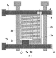
本発明実施例に係る有機薄膜トランジスタ(OTFT)アレイ基板は、図1及び図2(図1のA−A’に沿う断面図)に示すように、透明基板1上に形成される(画素ユニットの)画素構造を備え、
該画素構造は、ゲートライン7b、データライン2b、OTFT、画素電極2a、共通電極9及び共通電極線7cを備える。
An organic thin film transistor (OTFT) array substrate according to an embodiment of the present invention is formed on a transparent substrate 1 (a pixel unit) as shown in FIGS. 1 and 2 (a cross-sectional view taken along line AA ′ in FIG. 1). ) With pixel structure,
The pixel structure includes a
前記OTFTは、ゲート電極7a、ゲート絶縁層6、有機半導体層5、ソース電極2c及びドレイン電極2dを備える。
The OTFT includes a
前記データライン2b、前記ソース電極2c、前記ドレイン電極2d及び前記画素電極2aの上方に、第1のバンク絶縁層4及び第2のバンク絶縁層8は、下から上へ順に設置されている。
Above the
前記第1のバンク絶縁層4上に、第1のビアホール4a、第1の開口4b及び第2の開口4cが設けられている。ここで、バンク絶縁層上に形成されるビアホール及び開口に言及する場合、ビアホールはバンク絶縁層全体を貫通するが、開口はバンク絶縁層上に溝を形成し、溝の底部に一部のバンク絶縁層が保留されている。
A
前記第1の開口4bに、前記ゲートライン7bがプリントによって形成され、前記第2の開口4cに、前記共通電極線7cがプリントによって形成される。
The
前記第1のビアホール4aに、前記有機半導体層5、前記ゲート絶縁層6及び前記ゲート電極7aが下から上へ順にプリントによって形成され、前記ゲート電極7aが前記ゲートライン7bに接続され、前記有機半導体層5が前記ソース電極2c及び前記ドレイン電極2dに接続(接触)される。
In the first via
前記第2のバンク絶縁層8上に、互いに連通する第3の開口8a及び第2のビアホール8bが設けられ、前記第3の開口8aが前記画素電極2aの上方を櫛状に被覆することができる。
A
前記第2のビアホール8bは前記第2の開口4cに連通する。
The second via
前記第3の開口8a及び前記第2のビアホール8bに、共通電極9がプリントによって形成される。前記共通電極9と前記共通電極線7cは、前記第2のビアホール8bに接続することで接触する。
A
例えば、ソース電極2c、ドレイン電極2d、画素電極2a及びデータライン2bは、それぞれ同じ透明導電薄膜2をエッチングすることで形成される。ゲート電極7a、ゲートライン7b及び共通電極線7cは、それぞれプリントによって形成される。前記透明基板1はプラスチック基板、ガラス基板等であってよい。
For example, the
前記ソース電極2c、前記ドレイン電極2d及び前記データライン2bの表面に、金属薄膜3をさらに設けてもよい。
A metal
前記ソース電極2c及び前記ドレイン電極2dは前記第1のビアホール4aの中まで延び、前記ソース電極2c及び前記ドレイン電極2dは接続せずに互いに対向し、且つ前記ソース電極2cと前記ドレイン電極2dとの間の距離は前記第1のビアホール4aの両側の前記金属薄膜3の間の距離より小さくてもよい。
The source electrode 2c and the
前記有機半導体層5の厚みは、前記ソース電極2c及び前記ドレイン電極2dの厚みより大きくてもよい。
The thickness of the
前記有機半導体層5は、前記第1のビアホール4aの両側の、前記ソース電極2c及び前記ドレイン電極2dの側壁に接続されてもよい。
The
前記第1のバンク絶縁層4及び前記第2のバンク絶縁層8は、感光性の樹脂材料であってもよい。
The first
前記データライン2b、前記ソース電極2c、ドレイン電極2d、画素電極2a及び前記共通電極9の材料は、インジウムスズ酸化物、インジウム亜鉛酸化物等の導電材料であってもよい。
The material of the
前記有機半導体層5の材料は、チオフェン化合物、フタロシアニン化合物等であってもよい。
The material of the
前記ゲート絶縁層6の材料はポリビニルアルコールであってもよい。
The material of the
前記ゲート電極7aは導電性ポリチオフェン化合物、銅或いは銀のうちの1つであってもよい。
The
前記第1の開口4bに設けられる前記ゲートライン7b、前記第2の開口4cに設けられる前記共通電極線7c、及び前記第1のビアホール4aに設けられる前記ゲート電極7aの上表面は、前記第1のバンク絶縁層4の上表面と揃える。
The upper surface of the
前記OTFTアレイ基板のデータライン2b、ソース電極2c、及びドレイン電極2dの導電性を強くして、画素電極2aの充電速度を速くするように、図3及び図4(図4は図3のC−C’に沿う断面図である)に示すように、前記ソース電極2c、前記ドレイン電極2d及び前記データライン2bの表面に金属薄膜3を設けてもよい。前記金属薄膜3の材料は、アルミニウム、タングステン、クロム、タンタル、モリブデンまたは銅のうちの1つであってよい。
3 and 4 (FIG. 4 is a graph of FIG. 3) so that the
前記有機半導体層5は、ソース電極2cとドレイン電極2dを接続するとき、ソース電極2cとドレイン電極2dの側壁のみを接続するため、バーチャルコネクタの状況が発生しやすい。よって、有機半導体層5とソース電極2c及びドレイン電極2dとの接続面積を拡大し、バーチャルコネクタの状況を避けるように、前記ソース電極2c及び前記ドレイン電極2dを第1のビアホール4aの中まで延ばし、前記ソース電極2cと前記ドレイン電極2dとを接続させず、且つ前記ソース電極2cと前記ドレイン電極2dとの間の距離を前記第1のビアホール4aの両側の前記金属薄膜3の間の距離よりも小さくしてもよい。
Since the
本発明実施例は、前記OTFTアレイ基板に対応するように、以下のステップを備えるOTFTアレイ基板の製造方法を提供する。 The embodiment of the present invention provides a manufacturing method of an OTFT array substrate including the following steps so as to correspond to the OTFT array substrate.
ステップ100、透明基板上に透明導電薄膜を堆積する。
透明基板1上に透明導電薄膜2を堆積し、該透明導電薄膜2は、インジウムスズ酸化物、インジウム亜鉛酸化物等の導電材料であってよく、前記透明基板1は、ガラス基板、プラスチック基板等であってよい。
Step 100, depositing a transparent conductive thin film on a transparent substrate.
A transparent conductive
ステップ101、フォトレジストをスピンコーティングし、該フォトレジストのパターニング工程によって、データライン、ソース電極、ドレイン電極及び画素電極をエッチングするように形成し、残りの前記フォトレジストを除去する。
ここで、パターニング工程は、例えば、フォトレジストの塗布、露光、現像、エッチング、及びフォトレジストの除去等を備える。以下、再び贅言しない。
Step 101: spin-coating a photoresist, and patterning the photoresist to form a data line, a source electrode, a drain electrode, and a pixel electrode, and removing the remaining photoresist.
Here, the patterning step includes, for example, photoresist application, exposure, development, etching, and photoresist removal. Hereafter, I will not exaggerate again.
図5に示すように、透明導電薄膜2上にフォトレジスト10をスピンコーティングし、第1回のパターニング工程を行い、透明導電薄膜2をエッチングし、図6に示すように、画素電極2a、データライン2b、ソース電極2c及びドレイン電極2dを形成し、エッチングが完了したあと、剥離液によって残りのフォトレジスト10を除去する。
As shown in FIG. 5, a
ステップ102、感光性の樹脂を塗布し、第1のバンク絶縁層を固化して形成し、前記第1のバンク絶縁層上に、ダブルトーンマスク(例えば、ハーフトーンマスクまたはグレートーンマスク)によって露光・現像して、第1のビアホール、第1の開口及び第2の開口を形成し、前記第1のビアホールに有機半導体層をプリントによって形成し、前記有機半導体層上に前記ゲート絶縁層をプリントして、前記ゲート絶縁層上、前記第1の開口及び前記第2の開口に、前記ゲート電極、前記ゲートライン及び前記共通電極線をプリントによって形成し、前記有機半導体層が前記ソース電極と前記ドレイン電極を接続する。 Step 102: Applying a photosensitive resin, solidifying and forming a first bank insulating layer, and exposing the first bank insulating layer with a double tone mask (for example, a halftone mask or a gray tone mask). Development is performed to form a first via hole, a first opening, and a second opening, an organic semiconductor layer is formed in the first via hole by printing, and the gate insulating layer is printed on the organic semiconductor layer Then, the gate electrode, the gate line, and the common electrode line are formed by printing on the first insulating layer and the second opening on the gate insulating layer, and the organic semiconductor layer is formed on the source electrode and the second electrode. Connect the drain electrode.
図7に示すように、前記透明基板1上に感光性の樹脂の溶液を塗布し、前記感光性の樹脂はポリメタクリル酸エステルの溶液であってよい。該感光性の樹脂が透明基板1の表面を被覆した後、感光性の樹脂の中の溶剤を揮発させるように、例えば、約110℃で1〜30分のプリベークを行ってよい。
As shown in FIG. 7, a photosensitive resin solution may be applied on the
ダブルトーンマスクによって露光・現像した後、第1のビアホール4a、第1の開口4b及び第2の開口4cを形成する。例えば、ダブルトーンマスクを感光性の樹脂の上方に被覆し、該マスクがハーフトーンマスクまたはグレートーンマスクであり、そのハーフトーンまたはグレートーンの部分、即ち該マスクの一部透光領域は、感光性の樹脂の表面上に第1の開口4b及び第2の開口4cが形成される位置に対応し、マスクの完全透光しない領域は感光性の樹脂の完全保留領域に対応し、マスクの完全透光領域は感光性の樹脂の完全除去領域に対応し、第1のビアホール4aを形成することに用いられ、形成された第1のビアホール4aに、ソース電極2c及びドレイン電極2dの側壁が露出する。感光性の樹脂を露光して現像した後、例えば、約130℃で、1〜30分のポストベークを行い、第1のビアホール4a、第1の開口4b及び第2の開口4cを有する感光性の樹脂を固化することによって、第1のバンク絶縁層4を形成する。
After exposure and development using a double tone mask, a first via
第1のバンク絶縁層4を形成した後、例えば、プリンターのプリント設備を制御することで、第1のビアホール4a、第1の開口4b及び第2の開口4cでプリントする。まず、第1のビアホール4aで有機半導体層5を形成する有機半導体溶液をプリントする。そして、有機半導体溶剤を蒸発し、有機半導体層5を形成し、有機半導体溶剤を蒸発する過程では、有機半導体溶液の成分を均一化するように、アニールしてもよい。例えば、有機半導体層5と両側のソース電極2c及びドレイン電極2dの側壁とを十分に接触させるように、該有機半導体層5の厚みがソース電極2c及びドレイン電極2dよりも厚い。その後、有機半導体層5の表面でゲート電極絶縁層6を形成する溶液をプリントし、該ゲート絶縁層はポリビニルアルコールであってよく、該溶液を蒸発した後、ゲート電極絶縁層6を形成する。ゲート電極絶縁層6を形成した後、ゲート電極絶縁層6の表面、第1の開口4b及び第2の開口4cで、ゲート電極材料をそれぞれプリントし、前記ゲート電極材料の溶液または液体は導電性ポリチオフェン溶液、銅ペーストまたは銀ペーストであってよく、溶剤を蒸発してまたは該液体が凝固した後、ゲート電極7a、ゲートライン7b及び共通電極線7cをそれぞれ形成する。
After the first
感光性の樹脂上に、露光・現像によって、第1のビアホール4a、第1の開口4b及び第2の開口4cを有する第1のバンク絶縁層4を形成し、該第1のビアホール4a、第1の開口4b及び第2の開口4cを有する第1のバンク絶縁層4でプリントすることで、プリントする溶液または液体の範囲を制限することができ、バンク絶縁層に開口及びビアホールを設置することで、インクジェットプリント的な精確さを確保し、形成される有機半導体層5、ゲート絶縁層6、ゲート電極7a、信号線7b及び共通電極7cの精確さを保証し、有機半導体層5とソース電極2c及びドレイン電極2dとの接触面積を確保することができ、それによって、形成されるOTFTの性能が保証された。
A first
ステップ103、感光性の樹脂を再び塗布し、第2のバンク絶縁層を固化して形成し、前記第2のバンク絶縁層上に、露光・現像によって、互いに連通する第3の開口及び第2のビアホールを形成し、前記第3の開口は、前記画素電極の上方を櫛状に被覆し、前記第2のビアホール及び前記第3の開口にプリントによって共通電極を形成する。 Step 103, a photosensitive resin is applied again, and the second bank insulating layer is solidified to form a third opening and a second communicating with each other by exposure and development on the second bank insulating layer. The third opening covers the pixel electrode in a comb shape, and forms a common electrode by printing in the second via hole and the third opening.
図2に示すように、第1のバンク絶縁層4上に感光性の樹脂を再び塗布し、該感光性の樹脂が第1のバンク絶縁層4を被覆した後、感光性の樹脂の溶剤を揮発するように、例えば、約110℃で1〜30分のプリベークを行い、該感光性の樹脂を露光・現像して、互いに連通する第3の開口8a及び第2のビアホール8bを形成する。前記第2のビアホール8bは第2の開口4cと連通し、前記第3の開口8aは前記画素電極2aの上方に櫛状に被覆してよい。そして、例えば、約110℃で1〜30分のポストベークを行い、第2のバンク絶縁層8を固化して形成し、前記第2のビアホール8b及び第3の開口8aで共通電極9を形成する溶液をプリントし、溶剤を蒸発し、共通電極9を形成する。
As shown in FIG. 2, a photosensitive resin is applied again on the first
第2のバンク絶縁層8の第2のビアホール8b及び第3の開口8aで共通電極9を形成する溶液をプリントするため、共通電極9を形成する溶液の拡散が制限され、画素構造の精確さが確保され、画素の表示性能が保証された。
Since the solution for forming the
インクジェットプリント工程は、パターンを形成するためのインク滴(ゲート電極7a、ゲート絶縁層6、有機半導体層5、ゲートライン7b、共通電極線7c及び共通電極9を形成する材料)を、パターンを形成しようとする領域にプリントし、所要のパターンを形成する工程である。この工程はパターン化された層構造を直接に形成する方法であるため、プリントによって有機薄膜トランジスタアレイ基板を製造することで、工程を簡単化し、材料を節約し、コストを低下し、生産率を向上させることができるとともに、有機半導体層5と、ソース電極2c及びドレイン電極2dとの接触面積を確保することができ、そのパターンの高精度が薄膜トランジスタの性能を向上させることに寄与できる。また、インクジェットプリント工程によって共通電極線を製造することで、櫛状の共通電極のパターンを精確に形成することができ、その表示品質が確保された。
Ink jet printing process forms ink droplets (materials for forming
本実施例に係るOTFTアレイ基板では、画素電極を充電する速度は液晶ディスプレイスクリーンの表示効果に影響した。データライン2bの共通電極2aに対する充電速度を速くするため、前記透明基板上に透明導電薄膜を順に堆積した後、金属薄膜を堆積してもよい。
In the OTFT array substrate according to the present example, the speed of charging the pixel electrode affected the display effect of the liquid crystal display screen. In order to increase the charging speed for the
透明基板1上に透明導電薄膜2を堆積した後、図8に示すように、透明導電薄膜2の表面に金属薄膜3を堆積する。この堆積が例えばスパッタ設備で行われ、不活性気体のプラズマを加速してターゲットに衝突させる。ターゲットから衝突されて出た原子顆粒は電界及び磁場の作用によって、透明導電薄膜2上に均一に付着され、金属薄膜3を形成する。該金属薄膜3の材料は、アルミニウム、タングステン、クロム、タンタル、モリブデンまたは銅の1つであってよい。
After depositing the transparent conductive
前記金属薄膜3を形成した後、前記のように、フォトレジストをスピンコーティングし、該フォトレジストのパターニング工程によって、データライン、ソース電極、ドレイン電極及び画素電極をエッチングして形成し、残りの前記フォトレジストを除去してもよい。以下、図9〜図11を参照しながら、1つの具体的の例示を説明する。
After the metal
ステップ200、フォトレジストをスピンコーティングし、ダブルトーンマスクによってパターニング工程を行い、前記フォトレジスト上に完全保留領域、一部保留領域及び完全除去領域を形成する。 Step 200, spin-coating a photoresist and performing a patterning process using a double tone mask to form a completely reserved area, a partially reserved area and a completely removed area on the photoresist.
前記金属薄膜3上にフォトレジストをスピンコーティングし、ダブルトーンマスクによってパターニング工程を行い、露光・現像したあと、フォトレジスト上に図9に示す構造を形成し、即ち、前記フォトレジスト上にフォトレジスト完全保留領域10a、一部保留領域10b及び完全除去領域10cを形成する。完全保留領域10aは、マスク上における完全に透光しない遮蔽領域に対応し、一部保留領域10bは、マスク上におけるハーフトーンまたはグレートーンマスクの一部透光領域に対応し、完全除去領域10cは、マスク上における完全透光領域に対応する。ここで、ポジティブフォトレジストを例として説明する。
A photoresist is spin-coated on the metal
ステップ201、データライン、ソース電極、ドレイン電極及び画素電極をエッチングによって形成し、前記データライン、ソース電極、ドレイン電極及び画素電極の表面上の前記金属薄膜を保留する。
例えば、前記透明基板1をエッチングチャンバーに置いてエッチングする。まず、フォトレジスト10の完全除去領域10cの下方の金属薄膜3及び透明導電薄膜2をエッチングして除去し、図10に示すように、透明導電薄膜2から形成されたデータライン2b、ソース電極2c、ドレイン電極2d及び画素電極2aを形成するとともに、データライン2b、ソース電極2c、ドレイン電極2d及び画素電極2a上の金属薄膜3を保留する。
Step 201: Data lines, source electrodes, drain electrodes and pixel electrodes are formed by etching, and the metal thin film on the surfaces of the data lines, source electrodes, drain electrodes and pixel electrodes is retained.
For example, the
ステップ202、前記フォトレジストをアッシングして、前記一部保留領域のフォトレジストを除去し、エッチングによって、前記画素電極の表面の金属薄膜を除去する。 Step 202: Ashing the photoresist to remove the photoresist in the partially reserved region, and removing the metal thin film on the surface of the pixel electrode by etching.
図11に示すように、フォトレジスト10をアッシングし、前記一部保留領域10bのフォトレジストを除去し、一部保留領域10bの下方の金属薄膜3を露出させるとともに、完全保留領域10aのフォトレジストを一部保留する。そして、エッチングを再び行い、画素電極2aの表面に対応する金属薄膜3を除去し、下層の画素電極2aを露出させる。金属薄膜3をエッチングする過程では、金属のみをエッチングするエッチング液、またはエッチングガスによってエッチングし、あるいは、エッチングの時間を制御することによって、一部保留領域10bの金属薄膜3をエッチングし、透明導電薄膜2を保留する。
As shown in FIG. 11, the
最後に、形成されたOTFTアレイ基板は、図3及び図4に示すように、データライン2b、ソース電極2c及びドレイン電極2dの表面に金属薄膜3が付着しており、金属薄膜3のよい導電性能によって、透明導電薄膜2によって形成されたデータライン2b、ソース電極2c及びドレイン電極2dの導電性能を強化し、データライン2bがソース電極2c及びドレイン電極2dを介して画素電極2aに対する充電速度が向上した。
Finally, as shown in FIGS. 3 and 4, the formed OTFT array substrate has the metal
本発明実施例は、前記OTFTアレイ基板の製造方法に対応するように、表示装置を更に提供する。本実施例にかかる表示装置は、前記トップゲート型TFTアレイ基板を備える。前記表示装置は、液晶パネル、電子ペーパー、OLEDパネル、液晶テレビ、液晶ディスプレイ、デジタルフォトフレーム、携帯電話、タブレットPC等の表示機能を有するいずれの製品または部材に使用できる。 The embodiment of the present invention further provides a display device corresponding to the manufacturing method of the OTFT array substrate. The display device according to this example includes the top gate type TFT array substrate. The display device can be used for any product or member having a display function such as a liquid crystal panel, electronic paper, an OLED panel, a liquid crystal television, a liquid crystal display, a digital photo frame, a mobile phone, and a tablet PC.
該表示装置の1つの例示は液晶表示装置である。アレイ基板と対向基板が互いに対向して液晶セルを形成し、液晶セルに液晶材料が充填されている。該対向基板は、例えば、カラーフィルタ基板である。アレイ基板の各画素ユニットの画素電極は、表示操作を行うように、電界を印加して液晶材料の回転程度を制御するものである。幾つかの例示では、該液晶表示装置はアレイ基板にバックライトを提供するバックライトをさらに備える。 One example of the display device is a liquid crystal display device. The array substrate and the counter substrate face each other to form a liquid crystal cell, and the liquid crystal cell is filled with a liquid crystal material. The counter substrate is, for example, a color filter substrate. The pixel electrode of each pixel unit of the array substrate applies an electric field so as to perform a display operation and controls the degree of rotation of the liquid crystal material. In some examples, the liquid crystal display device further includes a backlight that provides a backlight to the array substrate.
本発明実施例に係るOTFTアレイ基板及びその製造方法によれば、感光性の樹脂によって第1のバンク絶縁層及び第2のバンク絶縁層をそれぞれ形成し、第1のバンク絶縁層及び第2のバンク絶縁層のビアホールと開口にプリントによって有機半導体層、ゲート絶縁層、ゲート電極、ゲートライン、共通電極及び共通電極線を形成することで、OTFTアレイ基板における有機半導体層、ゲート絶縁層、ゲート電極、ゲートライン、共通電極及び共通電極線等の構造が高速で効率よく形成され、有機半導体層、ゲート絶縁層、ゲート電極、ゲートライン、共通電極及び共通電極線等の構造を形成する材料が節約されたとともに、有機半導体層、ゲート絶縁層、ゲート電極、ゲートライン、共通電極及び共通電極線等の構造の精確さもよりよく制御された。 According to the OTFT array substrate and the manufacturing method thereof according to the embodiment of the present invention, the first bank insulating layer and the second bank insulating layer are respectively formed of photosensitive resin, and the first bank insulating layer and the second bank insulating layer are formed. Organic semiconductor layer, gate insulating layer, gate electrode in OTFT array substrate by forming organic semiconductor layer, gate insulating layer, gate electrode, gate line, common electrode and common electrode line by printing in via hole and opening of bank insulating layer Structures such as gate lines, common electrodes and common electrode lines are efficiently formed at high speed, and materials for forming structures such as organic semiconductor layers, gate insulating layers, gate electrodes, gate lines, common electrodes and common electrode lines are saved. In addition, the accuracy of the structure of the organic semiconductor layer, gate insulating layer, gate electrode, gate line, common electrode, common electrode line, etc. is better. It controlled.
以上は本発明の例示的な実施例だけであり、本発明の保護範囲は請求項により確定される。 The above are only exemplary embodiments of the present invention, and the protection scope of the present invention is determined by the claims.
1 透明基板
2 透明導電薄膜
2a 画素電極
2b データライン
2c ソース電極
2d ドレイン電極
3 金属薄膜
4 第1のバンク絶縁層
4a 第1のビアホール
4b 第1の開口
4c 第2の開口
5 有機半導体層
6 ゲート絶縁層
7a ゲート電極
7b ゲートライン
7c 共通電極線
8 第2のバンク絶縁層
8a 第3の開口
8b 第2のビアホール
9 共通電極
10 フォトレジスト
10a 完全保留領域
10b 一部保留領域
10c 完全除去領域
1
Claims (16)
前記有機薄膜トランジスタは、ゲート電極、ゲート絶縁層、有機半導体層、ソース電極及びドレイン電極を備え、
前記データライン、前記ソース電極、前記ドレイン電極及び前記画素電極の上方に、第1のバンク絶縁層及び第2のバンク絶縁層が下から上へ順に配置され、
前記第1のバンク絶縁層上に、第1のビアホール、第1の開口及び第2の開口が設けられ、
前記ソース電極及び前記ドレイン電極は前記第1のビアホールの両側に位置し、
前記第1の開口に、前記ゲートラインがプリントによって形成され、前記第2の開口に、前記共通電極線がプリントによって形成され、
前記第1のビアホールに、前記有機半導体層、前記ゲート絶縁層及び前記ゲート電極が下から上へ順にプリントによって形成され、前記ゲート電極が前記ゲートラインに接続され、前記有機半導体層が前記ソース電極とドレイン電極を接続し、
前記第2のバンク絶縁層上に、互いに連通する第3の開口及び第2のビアホールが設けられ、前記第2のビアホールが前記第2の開口と連通し、
前記第3の開口及び前記第2のビアホールに、共通電極がプリントによって形成され、前記共通電極は前記第2のビアホールを介して前記共通電極線と接続することを特徴とする有機薄膜トランジスタアレイ基板。 An organic thin film transistor array substrate comprising a pixel structure formed on a transparent substrate, the pixel structure comprising a gate line, a data line, an organic thin film transistor, a pixel electrode, a common electrode line and a common electrode,
The organic thin film transistor includes a gate electrode, a gate insulating layer, an organic semiconductor layer, a source electrode and a drain electrode,
A first bank insulating layer and a second bank insulating layer are disposed in order from the bottom to the top above the data line, the source electrode, the drain electrode, and the pixel electrode,
A first via hole, a first opening, and a second opening are provided on the first bank insulating layer,
The source electrode and the drain electrode are located on both sides of the first via hole,
The gate line is formed by printing in the first opening, the common electrode line is formed by printing in the second opening,
In the first via hole, the organic semiconductor layer, the gate insulating layer, and the gate electrode are formed by printing sequentially from bottom to top, the gate electrode is connected to the gate line, and the organic semiconductor layer is the source electrode And drain electrode ,
A third opening and a second via hole that communicate with each other are provided on the second bank insulating layer, and the second via hole communicates with the second opening,
An organic thin film transistor array substrate , wherein a common electrode is formed by printing in the third opening and the second via hole, and the common electrode is connected to the common electrode line through the second via hole .
透明基板上に透明導電薄膜を堆積し、パターニング工程によってデータライン、ソース電極、ドレイン電極及び画素電極を形成する工程と、
感光性の樹脂を塗布し、第1のバンク絶縁層を固化して形成し、前記第1のバンク絶縁層を露光・現像し、第1のビアホール、第1の開口及び第2の開口を形成し、前記第1のビアホールに有機半導体層をプリントによって形成し、前記有機半導体層上にゲート絶縁層をプリントし、前記ゲート絶縁層上、前記第1の開口及び前記第2の開口に、ゲート電極、ゲートライン及び共通電極線をプリントによって形成し、前記有機半導体層で前記ソース電極と前記ドレイン電極を接続する工程と、
感光性の樹脂を再び塗布し、第2のバンク絶縁層を固化して形成し、前記第2のバンク絶縁層に、露光・現像によって、互いに連通する第3の開口と第2のビアホールを形成し、前記第3の開口が前記画素電極の上方に位置し、且つ櫛状に配列され、前記第2のビアホール及び前記第3の開口に、共通電極をプリントによって形成する工程と、を備えることを特徴とする有機薄膜トランジスタアレイ基板の製造方法。 A method of manufacturing an organic thin film transistor array substrate,
Depositing a transparent conductive thin film on a transparent substrate and forming a data line, a source electrode, a drain electrode and a pixel electrode by a patterning process;
A photosensitive resin is applied, the first bank insulating layer is solidified, and the first bank insulating layer is exposed and developed to form a first via hole, a first opening, and a second opening. and an organic semiconductor layer was formed by printing on the first via hole, the organic semiconductor layer by printing gate insulating layer, the gate insulating layer, the first opening and the second opening Forming a gate electrode, a gate line and a common electrode line by printing, and connecting the source electrode and the drain electrode in the organic semiconductor layer;
A photosensitive resin is applied again, the second bank insulating layer is solidified, and a third opening and a second via hole are formed in the second bank insulating layer by exposure and development. And the third opening is positioned above the pixel electrode and arranged in a comb shape, and a common electrode is formed in the second via hole and the third opening by printing. A method for producing an organic thin film transistor array substrate, characterized in that:
金属薄膜を堆積する工程をさらに備え、
前記パターニング工程によってデータライン、ソース電極、ドレイン電極及び画素電極を形成する工程は、
フォトレジストをスピンコーティングし、ダブルトーンマスクによって露光・現像して、前記フォトレジスト上に完全保留領域、一部保留領域及び完全除去領域を形成する工程と、
データライン、ソース電極、ドレイン電極及び画素電極をエッチングによって形成し、前記データライン、ソース電極、ドレイン電極及び画素電極の表面の前記金属薄膜を保留する工程と、
前記フォトレジストをアッシングし、前記一部保留領域を除去し、エッチングによって前記画素電極の表面の金属薄膜を除去し、残りの前記フォトレジストを剥離する工程と、を備えることを特徴とする請求項13に記載の有機薄膜トランジスタアレイ基板の製造方法。 After depositing a transparent conductive thin film on the transparent substrate,
Further comprising depositing a metal thin film,
Forming the data line, the source electrode, the drain electrode, and the pixel electrode by the patterning step;
Spin coating the photoresist, exposing and developing with a double-tone mask to form a completely reserved area, a partially reserved area and a completely removed area on the photoresist;
Forming a data line, a source electrode, a drain electrode and a pixel electrode by etching, and retaining the metal thin film on the surface of the data line, the source electrode, the drain electrode and the pixel electrode;
The method includes: ashing the photoresist; removing the partial reserved region; removing a metal thin film on a surface of the pixel electrode by etching; and stripping the remaining photoresist. 14. A method for producing an organic thin film transistor array substrate according to 13 .
Applications Claiming Priority (5)
| Application Number | Priority Date | Filing Date | Title |
|---|---|---|---|
| CN201210123042.5 | 2012-04-24 | ||
| CN201210123042 | 2012-04-24 | ||
| CN201210269320.8 | 2012-07-30 | ||
| CN201210269320.8A CN102789106B (en) | 2012-04-24 | 2012-07-30 | Organic thin film transistor array substrate, preparation method thereof and display device |
| PCT/CN2012/086222 WO2013159538A1 (en) | 2012-04-24 | 2012-12-07 | Organic thin film transistor array substrate and preparation method thereof, and display device |
Publications (2)
| Publication Number | Publication Date |
|---|---|
| JP2015520940A JP2015520940A (en) | 2015-07-23 |
| JP6049111B2 true JP6049111B2 (en) | 2016-12-21 |
Family
ID=47154547
Family Applications (1)
| Application Number | Title | Priority Date | Filing Date |
|---|---|---|---|
| JP2015507339A Active JP6049111B2 (en) | 2012-04-24 | 2012-12-07 | Organic thin film transistor array substrate, method for manufacturing the same, and display device |
Country Status (6)
| Country | Link |
|---|---|
| US (1) | US9281353B2 (en) |
| EP (1) | EP2672316B1 (en) |
| JP (1) | JP6049111B2 (en) |
| KR (1) | KR101485720B1 (en) |
| CN (1) | CN102789106B (en) |
| WO (1) | WO2013159538A1 (en) |
Families Citing this family (9)
| Publication number | Priority date | Publication date | Assignee | Title |
|---|---|---|---|---|
| CN102789106B (en) * | 2012-04-24 | 2015-01-07 | 京东方科技集团股份有限公司 | Organic thin film transistor array substrate, preparation method thereof and display device |
| JP2015023161A (en) * | 2013-07-19 | 2015-02-02 | ソニー株式会社 | THIN FILM TRANSISTOR, MANUFACTURING METHOD THEREOF, AND ELECTRONIC DEVICE |
| CN104393019B (en) * | 2014-11-07 | 2017-11-10 | 京东方科技集团股份有限公司 | A kind of display base plate and preparation method thereof, display device |
| KR101712246B1 (en) * | 2014-12-05 | 2017-03-06 | 엘지디스플레이 주식회사 | Self-capacitive touch sensor integrated type display device |
| US9780973B2 (en) | 2015-03-02 | 2017-10-03 | Nxp Usa, Inc. | Channel estimation system for wireless communication system |
| CN104749845A (en) * | 2015-04-17 | 2015-07-01 | 合肥京东方光电科技有限公司 | Array substrate and manufacturing method thereof and display device |
| KR102591636B1 (en) * | 2016-03-24 | 2023-10-20 | 삼성디스플레이 주식회사 | Organic light-emitting display apparatus |
| CN109154749A (en) * | 2017-04-01 | 2019-01-04 | 京东方科技集团股份有限公司 | Array substrate, liquid crystal display panel and liquid crystal display device |
| KR20200071511A (en) * | 2018-12-11 | 2020-06-19 | 엘지디스플레이 주식회사 | Organic light emitting display device |
Family Cites Families (19)
| Publication number | Priority date | Publication date | Assignee | Title |
|---|---|---|---|---|
| KR100852830B1 (en) * | 2002-07-29 | 2008-08-18 | 비오이 하이디스 테크놀로지 주식회사 | Method for fabricating fringe field switching mode liquid crystal display |
| US7135724B2 (en) | 2004-09-29 | 2006-11-14 | International Business Machines Corporation | Structure and method for making strained channel field effect transistor using sacrificial spacer |
| KR101201017B1 (en) * | 2005-06-27 | 2012-11-13 | 엘지디스플레이 주식회사 | Liquid crystal display and fabricating method thereof |
| KR20070063300A (en) * | 2005-12-14 | 2007-06-19 | 삼성전자주식회사 | Organic thin film transistor array panel and manufacturing method thereof |
| KR101193381B1 (en) | 2005-12-29 | 2012-10-19 | 엘지디스플레이 주식회사 | Method of fabricating liquid crystal display device |
| KR101244898B1 (en) * | 2006-06-28 | 2013-03-19 | 삼성디스플레이 주식회사 | Organic Thin Film Transistor Substrate And Fabricating Method Thereof |
| KR20080030155A (en) * | 2006-09-29 | 2008-04-04 | 삼성전자주식회사 | Display device and manufacturing method thereof |
| JP5216204B2 (en) * | 2006-10-31 | 2013-06-19 | 株式会社半導体エネルギー研究所 | Liquid crystal display device and manufacturing method thereof |
| KR101389219B1 (en) * | 2006-12-29 | 2014-04-24 | 엘지디스플레이 주식회사 | Liquid Crystal Display Panel and Manufacturing Method thereof |
| US20080258138A1 (en) * | 2007-04-23 | 2008-10-23 | Samsung Electronics Co., Ltd. | Thin film transistor array panel and fabricating method thereof, and flat panel display with the same |
| KR101326129B1 (en) | 2007-07-24 | 2013-11-06 | 삼성디스플레이 주식회사 | Organic thin film transistor array panel and method for manufacturing the same |
| TWI509673B (en) | 2007-09-05 | 2015-11-21 | 尼康股份有限公司 | A manufacturing method of a display element, a manufacturing apparatus for a display element, and a display device |
| KR101264722B1 (en) | 2007-09-20 | 2013-05-15 | 엘지디스플레이 주식회사 | Method for manufacturing Liquid Crystal Display Device |
| CN101556417B (en) * | 2008-04-11 | 2010-12-01 | 北京京东方光电科技有限公司 | FFS type TFT-LCD array substrate structure and manufacture method thereof |
| KR20090124546A (en) * | 2008-05-30 | 2009-12-03 | 엘지디스플레이 주식회사 | Method for manufacturing organic thin film transistor substrate |
| JP4618337B2 (en) * | 2008-06-17 | 2011-01-26 | ソニー株式会社 | Display device and manufacturing method thereof, and semiconductor device and manufacturing method thereof |
| CN102742357A (en) * | 2010-08-06 | 2012-10-17 | 松下电器产业株式会社 | Organic EL display panel, display device, and method for manufacturing organic EL display panel |
| CN102789106B (en) * | 2012-04-24 | 2015-01-07 | 京东方科技集团股份有限公司 | Organic thin film transistor array substrate, preparation method thereof and display device |
| CN107289106A (en) | 2016-04-12 | 2017-10-24 | 江阴市富明机械有限公司 | Closure is not glued with handled |
-
2012
- 2012-07-30 CN CN201210269320.8A patent/CN102789106B/en active Active
- 2012-12-07 WO PCT/CN2012/086222 patent/WO2013159538A1/en not_active Ceased
- 2012-12-07 EP EP12830908.5A patent/EP2672316B1/en active Active
- 2012-12-07 JP JP2015507339A patent/JP6049111B2/en active Active
- 2012-12-07 US US13/824,540 patent/US9281353B2/en active Active
- 2012-12-07 KR KR20137009807A patent/KR101485720B1/en active Active
Also Published As
| Publication number | Publication date |
|---|---|
| EP2672316A1 (en) | 2013-12-11 |
| US9281353B2 (en) | 2016-03-08 |
| KR101485720B1 (en) | 2015-01-22 |
| WO2013159538A1 (en) | 2013-10-31 |
| JP2015520940A (en) | 2015-07-23 |
| CN102789106A (en) | 2012-11-21 |
| US20140110677A1 (en) | 2014-04-24 |
| EP2672316B1 (en) | 2020-05-06 |
| EP2672316A4 (en) | 2015-09-16 |
| CN102789106B (en) | 2015-01-07 |
| KR20130143570A (en) | 2013-12-31 |
Similar Documents
| Publication | Publication Date | Title |
|---|---|---|
| JP6049111B2 (en) | Organic thin film transistor array substrate, method for manufacturing the same, and display device | |
| JP6342132B2 (en) | Array substrate, display panel, and array substrate manufacturing method | |
| CN102629664B (en) | Array substrate and manufacturing method thereof, and display apparatus | |
| CN104216183B (en) | A kind of array base palte and preparation method thereof, display device | |
| US20160043102A1 (en) | Array Substrate and Method for Manufacturing the Same, and Display Device | |
| JP6818554B2 (en) | Array board manufacturing method, array board and display device | |
| CN102707523A (en) | Manufacturing method of array substrate as well as array substrate and display device | |
| CN103309105B (en) | Array base palte and preparation method thereof, display device | |
| US10481445B2 (en) | Array substrate and fabrication method thereof, and display device | |
| CN103439840A (en) | Array substrate, display device and method for manufacturing array substrate | |
| WO2014153958A1 (en) | Array substrate, method for manufacturing array substrate and display device | |
| US9690146B2 (en) | Array substrate, its manufacturing method, and display device | |
| CN103681765B (en) | Display floater and preparation method thereof, display unit | |
| US9019462B2 (en) | Array substrate and method for manufacturing the same, and display device | |
| CN101097924A (en) | Thin film transistor array substrate and manufacturing method thereof | |
| CN111679517A (en) | Display panel, manufacturing method thereof and display device | |
| US20120241746A1 (en) | Electrophoresis display and manufacturing method | |
| CN102854681B (en) | The manufacture method of a kind of array base palte, display device and array base palte | |
| CN114779546B (en) | Array substrate, preparation method thereof, liquid crystal display panel and display device | |
| CN110161762B (en) | Array substrate, manufacturing method thereof, and display panel | |
| CN117270254A (en) | Display panel, manufacturing method and display device thereof | |
| CN103700664A (en) | Array substrate as well as manufacturing method and display device thereof |
Legal Events
| Date | Code | Title | Description |
|---|---|---|---|
| A621 | Written request for application examination |
Free format text: JAPANESE INTERMEDIATE CODE: A621 Effective date: 20151201 |
|
| A977 | Report on retrieval |
Free format text: JAPANESE INTERMEDIATE CODE: A971007 Effective date: 20160628 |
|
| A131 | Notification of reasons for refusal |
Free format text: JAPANESE INTERMEDIATE CODE: A131 Effective date: 20160704 |
|
| A521 | Request for written amendment filed |
Free format text: JAPANESE INTERMEDIATE CODE: A523 Effective date: 20161003 |
|
| TRDD | Decision of grant or rejection written | ||
| A01 | Written decision to grant a patent or to grant a registration (utility model) |
Free format text: JAPANESE INTERMEDIATE CODE: A01 Effective date: 20161024 |
|
| A61 | First payment of annual fees (during grant procedure) |
Free format text: JAPANESE INTERMEDIATE CODE: A61 Effective date: 20161117 |
|
| R150 | Certificate of patent or registration of utility model |
Ref document number: 6049111 Country of ref document: JP Free format text: JAPANESE INTERMEDIATE CODE: R150 |
|
| R250 | Receipt of annual fees |
Free format text: JAPANESE INTERMEDIATE CODE: R250 |
|
| R250 | Receipt of annual fees |
Free format text: JAPANESE INTERMEDIATE CODE: R250 |
|
| R250 | Receipt of annual fees |
Free format text: JAPANESE INTERMEDIATE CODE: R250 |
|
| R250 | Receipt of annual fees |
Free format text: JAPANESE INTERMEDIATE CODE: R250 |
|
| R250 | Receipt of annual fees |
Free format text: JAPANESE INTERMEDIATE CODE: R250 |
|
| R250 | Receipt of annual fees |
Free format text: JAPANESE INTERMEDIATE CODE: R250 |
|
| R250 | Receipt of annual fees |
Free format text: JAPANESE INTERMEDIATE CODE: R250 |