JP6049111B2 - 有機薄膜トランジスタアレイ基板及びその製造方法、並びに表示装置 - Google Patents
有機薄膜トランジスタアレイ基板及びその製造方法、並びに表示装置 Download PDFInfo
- Publication number
- JP6049111B2 JP6049111B2 JP2015507339A JP2015507339A JP6049111B2 JP 6049111 B2 JP6049111 B2 JP 6049111B2 JP 2015507339 A JP2015507339 A JP 2015507339A JP 2015507339 A JP2015507339 A JP 2015507339A JP 6049111 B2 JP6049111 B2 JP 6049111B2
- Authority
- JP
- Japan
- Prior art keywords
- electrode
- thin film
- insulating layer
- film transistor
- opening
- Prior art date
- Legal status (The legal status is an assumption and is not a legal conclusion. Google has not performed a legal analysis and makes no representation as to the accuracy of the status listed.)
- Active
Links
Images


Classifications
-
- H—ELECTRICITY
- H10—SEMICONDUCTOR DEVICES; ELECTRIC SOLID-STATE DEVICES NOT OTHERWISE PROVIDED FOR
- H10K—ORGANIC ELECTRIC SOLID-STATE DEVICES
- H10K19/00—Integrated devices, or assemblies of multiple devices, comprising at least one organic element specially adapted for rectifying, amplifying, oscillating or switching, covered by group H10K10/00
- H10K19/10—Integrated devices, or assemblies of multiple devices, comprising at least one organic element specially adapted for rectifying, amplifying, oscillating or switching, covered by group H10K10/00 comprising field-effect transistors
-
- G—PHYSICS
- G02—OPTICS
- G02F—OPTICAL DEVICES OR ARRANGEMENTS FOR THE CONTROL OF LIGHT BY MODIFICATION OF THE OPTICAL PROPERTIES OF THE MEDIA OF THE ELEMENTS INVOLVED THEREIN; NON-LINEAR OPTICS; FREQUENCY-CHANGING OF LIGHT; OPTICAL LOGIC ELEMENTS; OPTICAL ANALOGUE/DIGITAL CONVERTERS
- G02F1/00—Devices or arrangements for the control of the intensity, colour, phase, polarisation or direction of light arriving from an independent light source, e.g. switching, gating or modulating; Non-linear optics
- G02F1/01—Devices or arrangements for the control of the intensity, colour, phase, polarisation or direction of light arriving from an independent light source, e.g. switching, gating or modulating; Non-linear optics for the control of the intensity, phase, polarisation or colour
- G02F1/13—Devices or arrangements for the control of the intensity, colour, phase, polarisation or direction of light arriving from an independent light source, e.g. switching, gating or modulating; Non-linear optics for the control of the intensity, phase, polarisation or colour based on liquid crystals, e.g. single liquid crystal display cells
- G02F1/133—Constructional arrangements; Operation of liquid crystal cells; Circuit arrangements
- G02F1/136—Liquid crystal cells structurally associated with a semi-conducting layer or substrate, e.g. cells forming part of an integrated circuit
- G02F1/1362—Active matrix addressed cells
- G02F1/136227—Through-hole connection of the pixel electrode to the active element through an insulation layer
-
- G—PHYSICS
- G02—OPTICS
- G02F—OPTICAL DEVICES OR ARRANGEMENTS FOR THE CONTROL OF LIGHT BY MODIFICATION OF THE OPTICAL PROPERTIES OF THE MEDIA OF THE ELEMENTS INVOLVED THEREIN; NON-LINEAR OPTICS; FREQUENCY-CHANGING OF LIGHT; OPTICAL LOGIC ELEMENTS; OPTICAL ANALOGUE/DIGITAL CONVERTERS
- G02F1/00—Devices or arrangements for the control of the intensity, colour, phase, polarisation or direction of light arriving from an independent light source, e.g. switching, gating or modulating; Non-linear optics
- G02F1/01—Devices or arrangements for the control of the intensity, colour, phase, polarisation or direction of light arriving from an independent light source, e.g. switching, gating or modulating; Non-linear optics for the control of the intensity, phase, polarisation or colour
- G02F1/13—Devices or arrangements for the control of the intensity, colour, phase, polarisation or direction of light arriving from an independent light source, e.g. switching, gating or modulating; Non-linear optics for the control of the intensity, phase, polarisation or colour based on liquid crystals, e.g. single liquid crystal display cells
- G02F1/133—Constructional arrangements; Operation of liquid crystal cells; Circuit arrangements
- G02F1/136—Liquid crystal cells structurally associated with a semi-conducting layer or substrate, e.g. cells forming part of an integrated circuit
- G02F1/1362—Active matrix addressed cells
- G02F1/136286—Wiring, e.g. gate line, drain line
-
- G—PHYSICS
- G02—OPTICS
- G02F—OPTICAL DEVICES OR ARRANGEMENTS FOR THE CONTROL OF LIGHT BY MODIFICATION OF THE OPTICAL PROPERTIES OF THE MEDIA OF THE ELEMENTS INVOLVED THEREIN; NON-LINEAR OPTICS; FREQUENCY-CHANGING OF LIGHT; OPTICAL LOGIC ELEMENTS; OPTICAL ANALOGUE/DIGITAL CONVERTERS
- G02F1/00—Devices or arrangements for the control of the intensity, colour, phase, polarisation or direction of light arriving from an independent light source, e.g. switching, gating or modulating; Non-linear optics
- G02F1/01—Devices or arrangements for the control of the intensity, colour, phase, polarisation or direction of light arriving from an independent light source, e.g. switching, gating or modulating; Non-linear optics for the control of the intensity, phase, polarisation or colour
- G02F1/13—Devices or arrangements for the control of the intensity, colour, phase, polarisation or direction of light arriving from an independent light source, e.g. switching, gating or modulating; Non-linear optics for the control of the intensity, phase, polarisation or colour based on liquid crystals, e.g. single liquid crystal display cells
- G02F1/133—Constructional arrangements; Operation of liquid crystal cells; Circuit arrangements
- G02F1/136—Liquid crystal cells structurally associated with a semi-conducting layer or substrate, e.g. cells forming part of an integrated circuit
- G02F1/1362—Active matrix addressed cells
- G02F1/136286—Wiring, e.g. gate line, drain line
- G02F1/136295—Materials; Compositions; Manufacture processes
-
- H—ELECTRICITY
- H10—SEMICONDUCTOR DEVICES; ELECTRIC SOLID-STATE DEVICES NOT OTHERWISE PROVIDED FOR
- H10K—ORGANIC ELECTRIC SOLID-STATE DEVICES
- H10K10/00—Organic devices specially adapted for rectifying, amplifying, oscillating or switching; Organic capacitors or resistors having potential barriers
- H10K10/40—Organic transistors
- H10K10/46—Field-effect transistors, e.g. organic thin-film transistors [OTFT]
- H10K10/462—Insulated gate field-effect transistors [IGFETs]
- H10K10/464—Lateral top-gate IGFETs comprising only a single gate
-
- H—ELECTRICITY
- H10—SEMICONDUCTOR DEVICES; ELECTRIC SOLID-STATE DEVICES NOT OTHERWISE PROVIDED FOR
- H10K—ORGANIC ELECTRIC SOLID-STATE DEVICES
- H10K59/00—Integrated devices, or assemblies of multiple devices, comprising at least one organic light-emitting element covered by group H10K50/00
- H10K59/10—OLED displays
- H10K59/12—Active-matrix OLED [AMOLED] displays
- H10K59/125—Active-matrix OLED [AMOLED] displays including organic TFTs [OTFT]
-
- H—ELECTRICITY
- H10—SEMICONDUCTOR DEVICES; ELECTRIC SOLID-STATE DEVICES NOT OTHERWISE PROVIDED FOR
- H10K—ORGANIC ELECTRIC SOLID-STATE DEVICES
- H10K71/00—Manufacture or treatment specially adapted for the organic devices covered by this subclass
- H10K71/20—Changing the shape of the active layer in the devices, e.g. patterning
- H10K71/231—Changing the shape of the active layer in the devices, e.g. patterning by etching of existing layers
-
- H—ELECTRICITY
- H10—SEMICONDUCTOR DEVICES; ELECTRIC SOLID-STATE DEVICES NOT OTHERWISE PROVIDED FOR
- H10K—ORGANIC ELECTRIC SOLID-STATE DEVICES
- H10K71/00—Manufacture or treatment specially adapted for the organic devices covered by this subclass
- H10K71/60—Forming conductive regions or layers, e.g. electrodes
- H10K71/611—Forming conductive regions or layers, e.g. electrodes using printing deposition, e.g. ink jet printing
-
- H—ELECTRICITY
- H10—SEMICONDUCTOR DEVICES; ELECTRIC SOLID-STATE DEVICES NOT OTHERWISE PROVIDED FOR
- H10K—ORGANIC ELECTRIC SOLID-STATE DEVICES
- H10K59/00—Integrated devices, or assemblies of multiple devices, comprising at least one organic light-emitting element covered by group H10K50/00
- H10K59/10—OLED displays
- H10K59/12—Active-matrix OLED [AMOLED] displays
- H10K59/131—Interconnections, e.g. wiring lines or terminals
-
- H—ELECTRICITY
- H10—SEMICONDUCTOR DEVICES; ELECTRIC SOLID-STATE DEVICES NOT OTHERWISE PROVIDED FOR
- H10K—ORGANIC ELECTRIC SOLID-STATE DEVICES
- H10K71/00—Manufacture or treatment specially adapted for the organic devices covered by this subclass
-
- H—ELECTRICITY
- H10—SEMICONDUCTOR DEVICES; ELECTRIC SOLID-STATE DEVICES NOT OTHERWISE PROVIDED FOR
- H10K—ORGANIC ELECTRIC SOLID-STATE DEVICES
- H10K71/00—Manufacture or treatment specially adapted for the organic devices covered by this subclass
- H10K71/10—Deposition of organic active material
- H10K71/12—Deposition of organic active material using liquid deposition, e.g. spin coating
- H10K71/13—Deposition of organic active material using liquid deposition, e.g. spin coating using printing techniques, e.g. ink-jet printing or screen printing
- H10K71/135—Deposition of organic active material using liquid deposition, e.g. spin coating using printing techniques, e.g. ink-jet printing or screen printing using ink-jet printing
Landscapes
- Physics & Mathematics (AREA)
- Engineering & Computer Science (AREA)
- Nonlinear Science (AREA)
- Microelectronics & Electronic Packaging (AREA)
- Mathematical Physics (AREA)
- Chemical & Material Sciences (AREA)
- Crystallography & Structural Chemistry (AREA)
- General Physics & Mathematics (AREA)
- Optics & Photonics (AREA)
- Manufacturing & Machinery (AREA)
- Thin Film Transistor (AREA)
- Liquid Crystal (AREA)
Description
透明基板上に透明導電薄膜を堆積し、パターニング工程によってデータライン、ソース電極、ドレイン電極及び画素電極を形成する工程と、
感光性の樹脂を塗布し、第1のバンク絶縁層を固化して形成し、前記第1のバンク絶縁層を露光・現像し、第1のビアホール、第1の開口及び第2の開口を形成し、前記第1のビアホールに、有機半導体層をプリントによって形成し、前記有機半導体層上に、前記ゲート絶縁層をプリントし、前記ゲート絶縁層上、前記第1の開口及び前記第2の開口に、前記ゲート電極、前記ゲートライン及び前記共通電極線をプリントによって形成し、前記有機半導体層を前記ソース電極及び前記ドレイン電極に接続する工程と、
感光性の樹脂を再び塗布し、第2のバンク絶縁層を固化して形成し、前記第2のバンク絶縁層に、露光・現像によって、互いに連通する第3の開口及び第2のビアホールを形成し、前記第3の開口が前記画素電極の上方を櫛状に被覆し、かつ櫛状に配列し、前記第2のビアホール及び前記第3の開口に、共通電極をプリントによって形成する工程と、を備える。
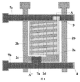
該画素構造は、ゲートライン7b、データライン2b、OTFT、画素電極2a、共通電極9及び共通電極線7cを備える。
透明基板1上に透明導電薄膜2を堆積し、該透明導電薄膜2は、インジウムスズ酸化物、インジウム亜鉛酸化物等の導電材料であってよく、前記透明基板1は、ガラス基板、プラスチック基板等であってよい。
ここで、パターニング工程は、例えば、フォトレジストの塗布、露光、現像、エッチング、及びフォトレジストの除去等を備える。以下、再び贅言しない。
例えば、前記透明基板1をエッチングチャンバーに置いてエッチングする。まず、フォトレジスト10の完全除去領域10cの下方の金属薄膜3及び透明導電薄膜2をエッチングして除去し、図10に示すように、透明導電薄膜2から形成されたデータライン2b、ソース電極2c、ドレイン電極2d及び画素電極2aを形成するとともに、データライン2b、ソース電極2c、ドレイン電極2d及び画素電極2a上の金属薄膜3を保留する。
2 透明導電薄膜
2a 画素電極
2b データライン
2c ソース電極
2d ドレイン電極
3 金属薄膜
4 第1のバンク絶縁層
4a 第1のビアホール
4b 第1の開口
4c 第2の開口
5 有機半導体層
6 ゲート絶縁層
7a ゲート電極
7b ゲートライン
7c 共通電極線
8 第2のバンク絶縁層
8a 第3の開口
8b 第2のビアホール
9 共通電極
10 フォトレジスト
10a 完全保留領域
10b 一部保留領域
10c 完全除去領域
Claims (16)
- 有機薄膜トランジスタアレイ基板であって、透明基板上に形成された画素構造を備え、前記画素構造は、ゲートライン、データライン、有機薄膜トランジスタ、画素電極、共通電極線及び共通電極を備え、
前記有機薄膜トランジスタは、ゲート電極、ゲート絶縁層、有機半導体層、ソース電極及びドレイン電極を備え、
前記データライン、前記ソース電極、前記ドレイン電極及び前記画素電極の上方に、第1のバンク絶縁層及び第2のバンク絶縁層が下から上へ順に配置され、
前記第1のバンク絶縁層上に、第1のビアホール、第1の開口及び第2の開口が設けられ、
前記ソース電極及び前記ドレイン電極は前記第1のビアホールの両側に位置し、
前記第1の開口に、前記ゲートラインがプリントによって形成され、前記第2の開口に、前記共通電極線がプリントによって形成され、
前記第1のビアホールに、前記有機半導体層、前記ゲート絶縁層及び前記ゲート電極が下から上へ順にプリントによって形成され、前記ゲート電極が前記ゲートラインに接続され、前記有機半導体層が前記ソース電極とドレイン電極を接続し、
前記第2のバンク絶縁層上に、互いに連通する第3の開口及び第2のビアホールが設けられ、前記第2のビアホールが前記第2の開口と連通し、
前記第3の開口及び前記第2のビアホールに、共通電極がプリントによって形成され、前記共通電極は前記第2のビアホールを介して前記共通電極線と接続することを特徴とする有機薄膜トランジスタアレイ基板。 - 前記ソース電極、前記ドレイン電極及び前記データラインの表面に金属薄膜が設けられることを特徴とする請求項1に記載の有機薄膜トランジスタアレイ基板。
- 前記ソース電極及び前記ドレイン電極は前記第1のビアホールの中まで延び、前記ソース電極と前記ドレイン電極とが接続せず、且つ前記ソース電極と前記ドレイン電極との間の距離は、前記第1のビアホールの両側の前記金属薄膜の間の距離よりも小さいことを特徴とする請求項2に記載の有機薄膜トランジスタアレイ基板。
- 前記有機半導体層の厚みは前記ソース電極及び前記ドレイン電極の厚みよりも大きいことを特徴とする請求項1〜3のいずれか1項に記載の有機薄膜トランジスタアレイ基板。
- 前記有機半導体層は、前記第1のビアホールの両側の前記ソース電極と前記ドレイン電極の側壁を接続することを特徴とする請求項1または2に記載の有機薄膜トランジスタアレイ基板。
- 前記第1のバンク絶縁層及び前記第2のバンク絶縁層は感光性の樹脂材料であることを特徴とする請求項1〜5のいずれか1項に記載の有機薄膜トランジスタアレイ基板。
- 前記データライン、前記ソース電極、前記ドレイン電極、前記画素電極及び前記共通電極の材料は、インジウムスズ酸化物またはインジウム亜鉛酸化物であることを特徴とする請求項1〜6のいずれか1項に記載の有機薄膜トランジスタアレイ基板。
- 前記有機半導体層の材料は、チオフェン化合物またはフタロシアニン化合物であることを特徴とする請求項1〜7のいずれか1項に記載の有機薄膜トランジスタアレイ基板。
- 前記ゲート絶縁層の材料はポリビニルアルコールであることを特徴とする請求項1〜8のいずれか1項に記載の有機薄膜トランジスタアレイ基板。
- 前記ゲート電極は、導電性ポリチオフェン化合物、銅または銀のうちの1つであることを特徴とする請求項1〜9のいずれか1項に記載の有機薄膜トランジスタアレイ基板。
- 前記第1の開口に設けられた前記ゲートライン、前記第2の開口に設けられた前記共通電極線、及び前記第1のビアホールに設けられた前記ゲート電極の上表面は、前記第1のバンク絶縁層の上表面と揃えることを特徴とする請求項1〜10のいずれか1項に記載の有機薄膜トランジスタアレイ基板。
- 前記金属薄膜の材料はアルミニウム、タングステン、クロム、タンタル、モリブデンまたは銅のうちの1つであることを特徴とする請求項2または3に記載の有機薄膜トランジスタアレイ基板。
- 有機薄膜トランジスタアレイ基板の製造方法であって、
透明基板上に透明導電薄膜を堆積し、パターニング工程によってデータライン、ソース電極、ドレイン電極及び画素電極を形成する工程と、
感光性の樹脂を塗布し、第1のバンク絶縁層を固化して形成し、前記第1のバンク絶縁層を露光・現像し、第1のビアホール、第1の開口及び第2の開口を形成し、前記第1のビアホールに有機半導体層をプリントによって形成し、前記有機半導体層上にゲート絶縁層をプリントし、前記ゲート絶縁層上、前記第1の開口及び前記第2の開口に、ゲート電極、ゲートライン及び共通電極線をプリントによって形成し、前記有機半導体層で前記ソース電極と前記ドレイン電極を接続する工程と、
感光性の樹脂を再び塗布し、第2のバンク絶縁層を固化して形成し、前記第2のバンク絶縁層に、露光・現像によって、互いに連通する第3の開口と第2のビアホールを形成し、前記第3の開口が前記画素電極の上方に位置し、且つ櫛状に配列され、前記第2のビアホール及び前記第3の開口に、共通電極をプリントによって形成する工程と、を備えることを特徴とする有機薄膜トランジスタアレイ基板の製造方法。 - 前記透明基板上に透明導電薄膜を堆積した後、
金属薄膜を堆積する工程をさらに備え、
前記パターニング工程によってデータライン、ソース電極、ドレイン電極及び画素電極を形成する工程は、
フォトレジストをスピンコーティングし、ダブルトーンマスクによって露光・現像して、前記フォトレジスト上に完全保留領域、一部保留領域及び完全除去領域を形成する工程と、
データライン、ソース電極、ドレイン電極及び画素電極をエッチングによって形成し、前記データライン、ソース電極、ドレイン電極及び画素電極の表面の前記金属薄膜を保留する工程と、
前記フォトレジストをアッシングし、前記一部保留領域を除去し、エッチングによって前記画素電極の表面の金属薄膜を除去し、残りの前記フォトレジストを剥離する工程と、を備えることを特徴とする請求項13に記載の有機薄膜トランジスタアレイ基板の製造方法。 - ダブルトーンマスクによって前記第1のバンク絶縁層を露光することを特徴とする請求項13または14に記載の有機薄膜トランジスタアレイ基板の製造方法。
- 表示装置であって、請求項1〜12のいずれか1項に記載の有機薄膜トランジスタアレイ基板を備えることを特徴とする表示装置。
Applications Claiming Priority (5)
| Application Number | Priority Date | Filing Date | Title |
|---|---|---|---|
| CN201210123042 | 2012-04-24 | ||
| CN201210123042.5 | 2012-04-24 | ||
| CN201210269320.8 | 2012-07-30 | ||
| CN201210269320.8A CN102789106B (zh) | 2012-04-24 | 2012-07-30 | 有机薄膜晶体管阵列基板及其制备方法以及显示装置 |
| PCT/CN2012/086222 WO2013159538A1 (zh) | 2012-04-24 | 2012-12-07 | 有机薄膜晶体管阵列基板及其制备方法以及显示装置 |
Publications (2)
| Publication Number | Publication Date |
|---|---|
| JP2015520940A JP2015520940A (ja) | 2015-07-23 |
| JP6049111B2 true JP6049111B2 (ja) | 2016-12-21 |
Family
ID=47154547
Family Applications (1)
| Application Number | Title | Priority Date | Filing Date |
|---|---|---|---|
| JP2015507339A Active JP6049111B2 (ja) | 2012-04-24 | 2012-12-07 | 有機薄膜トランジスタアレイ基板及びその製造方法、並びに表示装置 |
Country Status (6)
| Country | Link |
|---|---|
| US (1) | US9281353B2 (ja) |
| EP (1) | EP2672316B1 (ja) |
| JP (1) | JP6049111B2 (ja) |
| KR (1) | KR101485720B1 (ja) |
| CN (1) | CN102789106B (ja) |
| WO (1) | WO2013159538A1 (ja) |
Families Citing this family (9)
| Publication number | Priority date | Publication date | Assignee | Title |
|---|---|---|---|---|
| CN102789106B (zh) * | 2012-04-24 | 2015-01-07 | 京东方科技集团股份有限公司 | 有机薄膜晶体管阵列基板及其制备方法以及显示装置 |
| JP2015023161A (ja) * | 2013-07-19 | 2015-02-02 | ソニー株式会社 | 薄膜トランジスタおよびその製造方法ならびに電子機器 |
| CN104393019B (zh) * | 2014-11-07 | 2017-11-10 | 京东方科技集团股份有限公司 | 一种显示基板及其制备方法、显示装置 |
| KR101712246B1 (ko) * | 2014-12-05 | 2017-03-06 | 엘지디스플레이 주식회사 | 자기 정전용량식 터치 센서 일체형 표시장치 |
| US9780973B2 (en) | 2015-03-02 | 2017-10-03 | Nxp Usa, Inc. | Channel estimation system for wireless communication system |
| CN104749845A (zh) | 2015-04-17 | 2015-07-01 | 合肥京东方光电科技有限公司 | 一种阵列基板及其制作方法、显示装置 |
| KR102591636B1 (ko) | 2016-03-24 | 2023-10-20 | 삼성디스플레이 주식회사 | 유기발광 디스플레이 장치 |
| EP3607398B1 (en) * | 2017-04-01 | 2022-01-12 | BOE Technology Group Co., Ltd. | Array substrate, liquid crystal display panel and liquid crystal display apparatus |
| KR20200071511A (ko) * | 2018-12-11 | 2020-06-19 | 엘지디스플레이 주식회사 | 유기발광표시장치 |
Family Cites Families (19)
| Publication number | Priority date | Publication date | Assignee | Title |
|---|---|---|---|---|
| KR100852830B1 (ko) * | 2002-07-29 | 2008-08-18 | 비오이 하이디스 테크놀로지 주식회사 | 프린지 필드 스위칭 모드 액정표시장치의 제조방법 |
| US7135724B2 (en) * | 2004-09-29 | 2006-11-14 | International Business Machines Corporation | Structure and method for making strained channel field effect transistor using sacrificial spacer |
| KR101201017B1 (ko) * | 2005-06-27 | 2012-11-13 | 엘지디스플레이 주식회사 | 액정 표시 장치 및 그 제조 방법 |
| KR20070063300A (ko) * | 2005-12-14 | 2007-06-19 | 삼성전자주식회사 | 유기 박막 트랜지스터 표시판 및 그 제조 방법 |
| KR101193381B1 (ko) * | 2005-12-29 | 2012-10-19 | 엘지디스플레이 주식회사 | 액정표시장치의 제조방법 |
| KR101244898B1 (ko) * | 2006-06-28 | 2013-03-19 | 삼성디스플레이 주식회사 | 유기 박막 트랜지스터 기판 및 그 제조 방법 |
| KR20080030155A (ko) * | 2006-09-29 | 2008-04-04 | 삼성전자주식회사 | 표시 장치 및 그 제조 방법 |
| JP5216204B2 (ja) * | 2006-10-31 | 2013-06-19 | 株式会社半導体エネルギー研究所 | 液晶表示装置及びその作製方法 |
| KR101389219B1 (ko) * | 2006-12-29 | 2014-04-24 | 엘지디스플레이 주식회사 | 프린지 필드형 액정표시패널 및 그 제조 방법 |
| US20080258138A1 (en) | 2007-04-23 | 2008-10-23 | Samsung Electronics Co., Ltd. | Thin film transistor array panel and fabricating method thereof, and flat panel display with the same |
| KR101326129B1 (ko) | 2007-07-24 | 2013-11-06 | 삼성디스플레이 주식회사 | 유기 박막 트랜지스터 표시판 및 그 제조 방법 |
| TWI509673B (zh) | 2007-09-05 | 2015-11-21 | 尼康股份有限公司 | A manufacturing method of a display element, a manufacturing apparatus for a display element, and a display device |
| KR101264722B1 (ko) * | 2007-09-20 | 2013-05-15 | 엘지디스플레이 주식회사 | 액정표시장치의 제조방법 |
| CN101556417B (zh) * | 2008-04-11 | 2010-12-01 | 北京京东方光电科技有限公司 | Ffs型tft-lcd阵列基板结构及其制造方法 |
| KR20090124546A (ko) * | 2008-05-30 | 2009-12-03 | 엘지디스플레이 주식회사 | 유기 박막 트랜지스터 기판의 제조 방법 |
| JP4618337B2 (ja) * | 2008-06-17 | 2011-01-26 | ソニー株式会社 | 表示装置およびその製造方法、ならびに半導体装置およびその製造方法 |
| CN102742357A (zh) * | 2010-08-06 | 2012-10-17 | 松下电器产业株式会社 | 有机el显示面板、显示装置以及有机el显示面板的制造方法 |
| CN102789106B (zh) * | 2012-04-24 | 2015-01-07 | 京东方科技集团股份有限公司 | 有机薄膜晶体管阵列基板及其制备方法以及显示装置 |
| CN107289106A (zh) | 2016-04-12 | 2017-10-24 | 江阴市富明机械有限公司 | 带有把手的不粘密封盖 |
-
2012
- 2012-07-30 CN CN201210269320.8A patent/CN102789106B/zh active Active
- 2012-12-07 EP EP12830908.5A patent/EP2672316B1/en active Active
- 2012-12-07 KR KR20137009807A patent/KR101485720B1/ko active Active
- 2012-12-07 WO PCT/CN2012/086222 patent/WO2013159538A1/zh not_active Ceased
- 2012-12-07 US US13/824,540 patent/US9281353B2/en active Active
- 2012-12-07 JP JP2015507339A patent/JP6049111B2/ja active Active
Also Published As
| Publication number | Publication date |
|---|---|
| CN102789106B (zh) | 2015-01-07 |
| KR101485720B1 (ko) | 2015-01-22 |
| EP2672316A1 (en) | 2013-12-11 |
| EP2672316A4 (en) | 2015-09-16 |
| CN102789106A (zh) | 2012-11-21 |
| US20140110677A1 (en) | 2014-04-24 |
| WO2013159538A1 (zh) | 2013-10-31 |
| US9281353B2 (en) | 2016-03-08 |
| KR20130143570A (ko) | 2013-12-31 |
| EP2672316B1 (en) | 2020-05-06 |
| JP2015520940A (ja) | 2015-07-23 |
Similar Documents
| Publication | Publication Date | Title |
|---|---|---|
| JP6049111B2 (ja) | 有機薄膜トランジスタアレイ基板及びその製造方法、並びに表示装置 | |
| JP6342132B2 (ja) | アレイ基板、ディスプレイパネル及びアレイ基板の製造方法 | |
| CN102629664B (zh) | 一种阵列基板及其制作方法和显示装置 | |
| CN104216183B (zh) | 一种阵列基板及其制备方法、显示装置 | |
| US20160043102A1 (en) | Array Substrate and Method for Manufacturing the Same, and Display Device | |
| JP6818554B2 (ja) | アレイ基板の製造方法、アレイ基板および表示装置 | |
| CN102707523A (zh) | 一种阵列基板的制造方法、阵列基板及显示装置 | |
| CN103309105B (zh) | 阵列基板及其制备方法、显示装置 | |
| US10481445B2 (en) | Array substrate and fabrication method thereof, and display device | |
| CN103439840A (zh) | 一种阵列基板、显示装置及阵列基板的制造方法 | |
| WO2014153958A1 (zh) | 阵列基板、阵列基板的制造方法以及显示装置 | |
| US9690146B2 (en) | Array substrate, its manufacturing method, and display device | |
| CN103681765B (zh) | 显示面板及其制作方法、显示装置 | |
| US9019462B2 (en) | Array substrate and method for manufacturing the same, and display device | |
| CN101097924A (zh) | 薄膜晶体管阵列基板及其制造方法 | |
| CN111679517A (zh) | 一种显示面板及其制造方法,显示装置 | |
| US20120241746A1 (en) | Electrophoresis display and manufacturing method | |
| CN102854681B (zh) | 一种阵列基板、显示装置以及阵列基板的制造方法 | |
| CN114779546B (zh) | 阵列基板及其制备方法、液晶显示面板及显示装置 | |
| CN110161762B (zh) | 阵列基板及其制造方法、显示面板 | |
| CN117270254A (zh) | 显示面板及其制作方法、显示装置 | |
| CN103700664A (zh) | 阵列基板及其制作方法、显示装置 |
Legal Events
| Date | Code | Title | Description |
|---|---|---|---|
| A621 | Written request for application examination |
Free format text: JAPANESE INTERMEDIATE CODE: A621 Effective date: 20151201 |
|
| A977 | Report on retrieval |
Free format text: JAPANESE INTERMEDIATE CODE: A971007 Effective date: 20160628 |
|
| A131 | Notification of reasons for refusal |
Free format text: JAPANESE INTERMEDIATE CODE: A131 Effective date: 20160704 |
|
| A521 | Request for written amendment filed |
Free format text: JAPANESE INTERMEDIATE CODE: A523 Effective date: 20161003 |
|
| TRDD | Decision of grant or rejection written | ||
| A01 | Written decision to grant a patent or to grant a registration (utility model) |
Free format text: JAPANESE INTERMEDIATE CODE: A01 Effective date: 20161024 |
|
| A61 | First payment of annual fees (during grant procedure) |
Free format text: JAPANESE INTERMEDIATE CODE: A61 Effective date: 20161117 |
|
| R150 | Certificate of patent or registration of utility model |
Ref document number: 6049111 Country of ref document: JP Free format text: JAPANESE INTERMEDIATE CODE: R150 |
|
| R250 | Receipt of annual fees |
Free format text: JAPANESE INTERMEDIATE CODE: R250 |
|
| R250 | Receipt of annual fees |
Free format text: JAPANESE INTERMEDIATE CODE: R250 |
|
| R250 | Receipt of annual fees |
Free format text: JAPANESE INTERMEDIATE CODE: R250 |
|
| R250 | Receipt of annual fees |
Free format text: JAPANESE INTERMEDIATE CODE: R250 |
|
| R250 | Receipt of annual fees |
Free format text: JAPANESE INTERMEDIATE CODE: R250 |
|
| R250 | Receipt of annual fees |
Free format text: JAPANESE INTERMEDIATE CODE: R250 |
|
| R250 | Receipt of annual fees |
Free format text: JAPANESE INTERMEDIATE CODE: R250 |