JP6069237B2 - 電子機器 - Google Patents
電子機器 Download PDFInfo
- Publication number
- JP6069237B2 JP6069237B2 JP2014034940A JP2014034940A JP6069237B2 JP 6069237 B2 JP6069237 B2 JP 6069237B2 JP 2014034940 A JP2014034940 A JP 2014034940A JP 2014034940 A JP2014034940 A JP 2014034940A JP 6069237 B2 JP6069237 B2 JP 6069237B2
- Authority
- JP
- Japan
- Prior art keywords
- cover panel
- panel
- electronic device
- main surface
- reducing member
- Prior art date
- Legal status (The legal status is an assumption and is not a legal conclusion. Google has not performed a legal analysis and makes no representation as to the accuracy of the status listed.)
- Expired - Fee Related
Links
Images









Classifications
-
- H—ELECTRICITY
- H04—ELECTRIC COMMUNICATION TECHNIQUE
- H04B—TRANSMISSION
- H04B1/00—Details of transmission systems, not covered by a single one of groups H04B3/00 - H04B13/00; Details of transmission systems not characterised by the medium used for transmission
- H04B1/38—Transceivers, i.e. devices in which transmitter and receiver form a structural unit and in which at least one part is used for functions of transmitting and receiving
- H04B1/3827—Portable transceivers
- H04B1/3888—Arrangements for carrying or protecting transceivers
-
- G—PHYSICS
- G06—COMPUTING OR CALCULATING; COUNTING
- G06F—ELECTRIC DIGITAL DATA PROCESSING
- G06F1/00—Details not covered by groups G06F3/00 - G06F13/00 and G06F21/00
- G06F1/16—Constructional details or arrangements
- G06F1/1601—Constructional details related to the housing of computer displays, e.g. of CRT monitors, of flat displays
- G06F1/1605—Multimedia displays, e.g. with integrated or attached speakers, cameras, microphones
-
- G—PHYSICS
- G06—COMPUTING OR CALCULATING; COUNTING
- G06F—ELECTRIC DIGITAL DATA PROCESSING
- G06F1/00—Details not covered by groups G06F3/00 - G06F13/00 and G06F21/00
- G06F1/16—Constructional details or arrangements
- G06F1/1613—Constructional details or arrangements for portable computers
- G06F1/1626—Constructional details or arrangements for portable computers with a single-body enclosure integrating a flat display, e.g. Personal Digital Assistants [PDAs]
-
- G—PHYSICS
- G06—COMPUTING OR CALCULATING; COUNTING
- G06F—ELECTRIC DIGITAL DATA PROCESSING
- G06F1/00—Details not covered by groups G06F3/00 - G06F13/00 and G06F21/00
- G06F1/16—Constructional details or arrangements
- G06F1/1613—Constructional details or arrangements for portable computers
- G06F1/1633—Constructional details or arrangements of portable computers not specific to the type of enclosures covered by groups G06F1/1615 - G06F1/1626
- G06F1/1656—Details related to functional adaptations of the enclosure, e.g. to provide protection against EMI, shock, water, or to host detachable peripherals like a mouse or removable expansions units like PCMCIA cards, or to provide access to internal components for maintenance or to removable storage supports like CDs or DVDs, or to mechanically mount accessories
-
- H—ELECTRICITY
- H04—ELECTRIC COMMUNICATION TECHNIQUE
- H04M—TELEPHONIC COMMUNICATION
- H04M1/00—Substation equipment, e.g. for use by subscribers
- H04M1/02—Constructional features of telephone sets
- H04M1/0202—Portable telephone sets, e.g. cordless phones, mobile phones or bar type handsets
- H04M1/026—Details of the structure or mounting of specific components
- H04M1/0266—Details of the structure or mounting of specific components for a display module assembly
-
- H—ELECTRICITY
- H04—ELECTRIC COMMUNICATION TECHNIQUE
- H04M—TELEPHONIC COMMUNICATION
- H04M1/00—Substation equipment, e.g. for use by subscribers
- H04M1/02—Constructional features of telephone sets
- H04M1/0202—Portable telephone sets, e.g. cordless phones, mobile phones or bar type handsets
- H04M1/026—Details of the structure or mounting of specific components
- H04M1/0277—Details of the structure or mounting of specific components for a printed circuit board assembly
-
- H—ELECTRICITY
- H04—ELECTRIC COMMUNICATION TECHNIQUE
- H04M—TELEPHONIC COMMUNICATION
- H04M1/00—Substation equipment, e.g. for use by subscribers
- H04M1/02—Constructional features of telephone sets
- H04M1/18—Telephone sets specially adapted for use in ships, mines, or other places exposed to adverse environment
- H04M1/185—Improving the shock resistance of the housing, e.g. by increasing the rigidity
Landscapes
- Engineering & Computer Science (AREA)
- Theoretical Computer Science (AREA)
- Computer Hardware Design (AREA)
- Signal Processing (AREA)
- General Engineering & Computer Science (AREA)
- Human Computer Interaction (AREA)
- Physics & Mathematics (AREA)
- General Physics & Mathematics (AREA)
- Computer Networks & Wireless Communication (AREA)
- Multimedia (AREA)
- Telephone Set Structure (AREA)
- Casings For Electric Apparatus (AREA)
Description
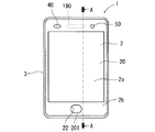
図1〜3は、それぞれ、実施の形態に係る電子機器1の外観を示す斜視図、前面図及び裏面図である。図4は図2に示される電子機器1の矢視A−Aにおける断面構造の概略を示す図である。図5は、電子機器1が備えるカバーパネル2の裏面図である。図5に示されるカバーパネル2には、電子機器1が備える圧電振動素子190及び表示パネル120が取り付けられている。本実施の形態に係る電子機器1は、例えば、スマートフォン等の携帯電話機である。
図6は電子機器1の電気的構成を主に示すブロック図である。図6に示されるように、電子機器1には、制御部100、無線通信部110、表示パネル120、タッチパネル130、近接センサ140及びマイク150が設けられている。さらに電子機器1には、前面側撮像部160、裏面側撮像部170、外部スピーカ180、圧電振動素子190、操作部200及び電池210が設けられている。電子機器1に設けられた、カバーパネル2以外のこれらの構成要素はケース3内に収められている。
図7,8は、それぞれ、圧電振動素子190の構造を示す上面図及び側面図である。図7,8に示されるように、圧電振動素子190は一方向に長い形状を成している。具体的には、圧電振動素子190は、平面視で長方形の細長い板状を成している。圧電振動素子190は、例えばバイモルフ構造を有している。圧電振動素子190は、シム材190cを介して互いに貼り合わされた第1圧電セラミック板190a及び第2圧電セラミック板190bを備えている。
本実施の形態に係る電子機器1では、圧電振動素子190がカバーパネル2を振動させることによって、当該カバーパネル2から気導音及び伝導音が使用者に伝達される。言い換えれば、圧電振動素子190自身の振動がカバーパネル2に伝わることにより、当該カバーパネル2から気導音及び伝導音が使用者に伝達される。
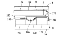
図12は、電子機器1の内部構成の一部を拡大して模式的に示す断面図である。裏面側撮像部170は電子機器1の上方に設けられ(図4,5も参照)、プリント基板260は裏面側撮像部170の下方に設けられる。
図12の例示では、隙間低減部材280のフレキ270側の外形が、フレキ270の湾曲部に沿った形状(例えば略半円状の形状)を有している。これにより、隙間低減部材280の厚み(カバーパネル2に垂直な方向における厚み)を、より増大することができる。よって、隙間低減部材280が薄い構造に比して、隙間低減部材280の変位を低減することができる。つまり、隙間低減部材280がカバーパネル2を支持する力を向上することができ、ひいてはカバーパネル2の割れを更に抑制できる。
フレキ270の幅と隙間低減部材280の幅とについて説明する。なおここでいう幅とは、フレキ270の延在方向(フレキ270に形成される配線の延在方向、ここでは上下方向)に垂直な方向における幅である。
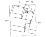
図12および図13の例示では、隙間低減部材280は、裏面側撮像部170を保持するホルダー288の一部である。ホルダー288は、例えば裏面側撮像部170の位置決め、保護あるいは固定のために設けられる。ホルダー288は、例えば裏面側撮像部170の周囲を囲っており、また裏面側撮像部170に対してカバーパネル2側から接触している。
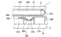
図14は、電子機器1の他の一例の内部構成を拡大して概略的に示す断面図である。図14の電子機器1は図12の電子機器1に比べて隙間低減部材282を更に備えている。隙間低減部材282はフレキ270よりも電子機器1の裏面10側に設けられており、フレキ270の湾曲部の少なくとも一部に接触する。つまり隙間低減部材280,282の間にフレキ270が位置する。隙間低減部材282の材質は固体であれば特に限定されないが、例えば絶縁材料等の樹脂である。隙間低減部材282は適宜に電子機器1に固定される。例えば隙間低減部材282はケース3に固定される。
図15は、電子機器1の他の一例の内部構成を拡大して概略的に示す断面図である。図15の電子機器1は図14の電子機器1に比べて隙間低減部材284を更に備えている。
図16の例示では、フレキ272の湾曲部のうちカバーパネル2側の部分に対して、カバーパネル2側から接触する隙間低減部材286が設けられている。隙間低減部材286は電子機器1(カバーパネル2以外の部材、例えばケース3など)に固定される。これによっても、カバーパネル2を支持することができるので、カバーパネル2の割れ(特に、平面視においてフレキ272の湾曲部と同じ位置のカバーパネル2の部分が、より強く押圧された場合に発生しうる割れ)を抑制できる。
2 カバーパネル
8,80 パネル
20 第1主面
21 第2主面
270,272 フレキシブルプリント配線板
280,282,284,286 隙間低減部材
Claims (6)
- 電子機器であって、
ケースと、
外側主面および内側主面を有し、前記外側主面を外側に向けて前記ケースに設けられた、サファイアから成るパネルと、
前記パネルの前記内側主面側において、平らに設けられた第1部分と、前記外側主面から前記内側主面への第1方向に前記第1部分よりも前記パネルから離れて設けられた第2部分とを有するケーブルと、
前記第2部分と前記パネルとの間に位置し、前記第1部分よりも前記パネルから前記第1方向に離れた部位を有する隙間低減部材と、
を備え、
前記ケーブルは、折り返すことなく延在する、電子機器。 - 前記パネルの前記内側主面に位置するタッチパネルと、
前記タッチパネルが有する主面のうち前記パネルと対向する主面とは逆側の主面に位置する表示部と、
をさらに備え、
前記隙間低減部材は、前記第2部分と前記表示部との間に位置している、請求項1記載の電子機器。 - 前記第2部分は、前記ケーブルにおいて前記パネルから前記第1方向に最も離れた第3部分を有し、
前記第3部分と前記パネルとの間に前記隙間低減部材の前記部位が位置している、請求項1または2に記載の電子機器。 - 前記第1部分と前記第2部分とは連続しており、
前記第2部分は、前記ケーブルが前記第1方向へ膨らむように前記第1部分から曲がる部位を含む、請求項1から3のいずれか一つに記載の電子機器。 - プリント基板を更に備え、
前記隙間低減部材は前記プリント基板と向かい合う、請求項1から4のいずれか一つに記載の電子機器。 - 前記ケーブルはフレキシブルプリント配線板であって、
前記隙間低減部材の幅は、前記フレキシブルプリント配線板の幅以上である、請求項1から5のいずれか一つに記載の電子機器。
Priority Applications (6)
| Application Number | Priority Date | Filing Date | Title |
|---|---|---|---|
| JP2014034940A JP6069237B2 (ja) | 2014-02-26 | 2014-02-26 | 電子機器 |
| US14/337,954 US8977329B1 (en) | 2014-02-26 | 2014-07-22 | Electronic apparatus |
| US14/616,577 US9438296B2 (en) | 2014-02-26 | 2015-02-06 | Electronic apparatus |
| EP15754808.2A EP3111293A1 (en) | 2014-02-26 | 2015-02-26 | Electronic apparatus |
| PCT/JP2015/001003 WO2015129274A1 (en) | 2014-02-26 | 2015-02-26 | Electronic apparatus |
| US15/253,698 US9991925B2 (en) | 2014-02-26 | 2016-08-31 | Electronic apparatus |
Applications Claiming Priority (1)
| Application Number | Priority Date | Filing Date | Title |
|---|---|---|---|
| JP2014034940A JP6069237B2 (ja) | 2014-02-26 | 2014-02-26 | 電子機器 |
Publications (2)
| Publication Number | Publication Date |
|---|---|
| JP2015162702A JP2015162702A (ja) | 2015-09-07 |
| JP6069237B2 true JP6069237B2 (ja) | 2017-02-01 |
Family
ID=52597896
Family Applications (1)
| Application Number | Title | Priority Date | Filing Date |
|---|---|---|---|
| JP2014034940A Expired - Fee Related JP6069237B2 (ja) | 2014-02-26 | 2014-02-26 | 電子機器 |
Country Status (4)
| Country | Link |
|---|---|
| US (3) | US8977329B1 (ja) |
| EP (1) | EP3111293A1 (ja) |
| JP (1) | JP6069237B2 (ja) |
| WO (1) | WO2015129274A1 (ja) |
Families Citing this family (6)
| Publication number | Priority date | Publication date | Assignee | Title |
|---|---|---|---|---|
| KR20170028164A (ko) * | 2015-09-03 | 2017-03-13 | 엘지전자 주식회사 | 이동 단말기 |
| WO2017139891A1 (en) * | 2016-02-17 | 2017-08-24 | Dalhousie University | Piezoelectric inertial actuator |
| CN108156288B (zh) * | 2018-01-02 | 2021-01-22 | 京东方科技集团股份有限公司 | 一种显示模组及其制备方法 |
| CN108418924B (zh) * | 2018-04-12 | 2020-01-24 | Oppo广东移动通信有限公司 | 壳体组件以及电子装置 |
| CN111064829B (zh) * | 2019-10-29 | 2021-12-28 | 华为技术有限公司 | 一种显示装置及终端设备 |
| CN114882794B (zh) * | 2022-05-23 | 2023-09-26 | 武汉华星光电半导体显示技术有限公司 | 显示模组 |
Family Cites Families (31)
| Publication number | Priority date | Publication date | Assignee | Title |
|---|---|---|---|---|
| JPH0639497Y2 (ja) * | 1988-08-23 | 1994-10-12 | ティアツク株式会社 | フレキシブルプリント基板用ホルダ |
| JPH0751746Y2 (ja) * | 1989-02-28 | 1995-11-22 | 日本精機株式会社 | 回路基板の接続装置 |
| JPH02132823U (ja) | 1989-04-12 | 1990-11-05 | ||
| JPH05335435A (ja) | 1992-05-29 | 1993-12-17 | Kyocera Corp | 半導体素子収納用パッケージ |
| JPH05333164A (ja) | 1992-06-02 | 1993-12-17 | Seiko Epson Corp | 時計用複層カバーガラス |
| JP3207079B2 (ja) | 1995-06-23 | 2001-09-10 | 京セラ株式会社 | 携帯通信機 |
| JP3754588B2 (ja) * | 1999-09-08 | 2006-03-15 | 富士通アクセス株式会社 | 光ケーブル保持具 |
| US6317330B1 (en) * | 2000-02-15 | 2001-11-13 | Bitmicro Networks, Inc. | Printed circuit board assembly |
| WO2002054723A1 (en) | 2000-12-29 | 2002-07-11 | Vertu Ltd | A casing |
| GB2374235B (en) | 2000-12-29 | 2004-09-22 | Nokia Mobile Phones Ltd | A casing |
| GB2377115B (en) | 2000-12-29 | 2005-06-22 | Nokia Mobile Phones Ltd | A casing for a personal communication device, comprising precious metals, precious stones or ceramics |
| JP4048117B2 (ja) | 2000-12-29 | 2008-02-13 | ベルツ リミテッド | ケース |
| JP2004517447A (ja) | 2000-12-29 | 2004-06-10 | ベルツ リミテッド | ケース |
| JP2005173393A (ja) | 2003-12-12 | 2005-06-30 | Seiko Epson Corp | 液晶表示装置および電子機器 |
| JP4172459B2 (ja) * | 2004-04-22 | 2008-10-29 | セイコーエプソン株式会社 | 電気光学装置及び電子機器 |
| JP2007004027A (ja) * | 2005-06-27 | 2007-01-11 | Optrex Corp | 画像表示装置 |
| US7684205B2 (en) * | 2006-02-22 | 2010-03-23 | General Dynamics Advanced Information Systems, Inc. | System and method of using a compliant lead interposer |
| JP5090710B2 (ja) | 2006-10-30 | 2012-12-05 | 京セラ株式会社 | 携帯電子機器 |
| US7677905B2 (en) * | 2006-12-13 | 2010-03-16 | Denso Corporation | Electronic device and manufacturing method of the same |
| JP2010072272A (ja) | 2008-09-18 | 2010-04-02 | Epson Imaging Devices Corp | 電気光学装置及び電子機器 |
| JP2010109680A (ja) * | 2008-10-30 | 2010-05-13 | Kyocera Corp | 携帯電子機器 |
| JP5212222B2 (ja) * | 2009-03-30 | 2013-06-19 | 富士通株式会社 | 携帯端末装置 |
| CN103563341B (zh) | 2011-06-03 | 2017-07-07 | 索尼电脑娱乐公司 | 便携式电子装置、便携式电子装置组及制造该装置的方法 |
| JP2012252610A (ja) * | 2011-06-03 | 2012-12-20 | Sony Computer Entertainment Inc | 携帯型電子機器、携帯型電子機器群、及び携帯型電子機器の製造方法 |
| JP5926950B2 (ja) | 2011-12-22 | 2016-05-25 | 京セラ株式会社 | 電子機器 |
| US10052848B2 (en) | 2012-03-06 | 2018-08-21 | Apple Inc. | Sapphire laminates |
| TW201345339A (zh) * | 2012-04-17 | 2013-11-01 | Tera Xtal Technology Corp | 觸控面板 |
| US9429997B2 (en) | 2012-06-12 | 2016-08-30 | Apple Inc. | Electronic device with wrapped display |
| TWI554914B (zh) * | 2012-06-27 | 2016-10-21 | 鴻海精密工業股份有限公司 | 觸控面板及觸摸式液晶顯示屏 |
| US20140023430A1 (en) | 2012-07-19 | 2014-01-23 | Apple Inc. | Attachment Techniques |
| US9221289B2 (en) | 2012-07-27 | 2015-12-29 | Apple Inc. | Sapphire window |
-
2014
- 2014-02-26 JP JP2014034940A patent/JP6069237B2/ja not_active Expired - Fee Related
- 2014-07-22 US US14/337,954 patent/US8977329B1/en not_active Expired - Fee Related
-
2015
- 2015-02-06 US US14/616,577 patent/US9438296B2/en not_active Expired - Fee Related
- 2015-02-26 WO PCT/JP2015/001003 patent/WO2015129274A1/en not_active Ceased
- 2015-02-26 EP EP15754808.2A patent/EP3111293A1/en not_active Withdrawn
-
2016
- 2016-08-31 US US15/253,698 patent/US9991925B2/en not_active Expired - Fee Related
Also Published As
| Publication number | Publication date |
|---|---|
| WO2015129274A1 (en) | 2015-09-03 |
| US8977329B1 (en) | 2015-03-10 |
| JP2015162702A (ja) | 2015-09-07 |
| US20150244409A1 (en) | 2015-08-27 |
| US9438296B2 (en) | 2016-09-06 |
| US20170054468A1 (en) | 2017-02-23 |
| US9991925B2 (en) | 2018-06-05 |
| EP3111293A1 (en) | 2017-01-04 |
Similar Documents
| Publication | Publication Date | Title |
|---|---|---|
| JP5865433B2 (ja) | 電子機器 | |
| JP6275566B2 (ja) | 電子機器 | |
| US9474174B2 (en) | Electronic apparatus | |
| JP5674895B1 (ja) | 電子機器 | |
| JP6367098B2 (ja) | 電子機器 | |
| JP6069237B2 (ja) | 電子機器 | |
| JP5865408B2 (ja) | 電子機器 | |
| JP5914426B2 (ja) | 電子機器 | |
| JP5852635B2 (ja) | 電子機器 | |
| JP5707454B2 (ja) | 電子機器 | |
| JP5981601B2 (ja) | 電子機器 | |
| JP6279314B2 (ja) | 電子機器 | |
| WO2016067888A1 (ja) | 電子機器 | |
| JP5937641B2 (ja) | 電子機器 | |
| JP6010680B2 (ja) | 電子機器 | |
| JP2015088836A (ja) | 電子機器 | |
| JP5744296B1 (ja) | 電子機器 | |
| JP6154041B2 (ja) | 電子機器 | |
| JP5925874B2 (ja) | 電子機器 | |
| JP6143838B2 (ja) | 電子機器 | |
| JP2015126283A (ja) | サファイアパネルおよびそれを用いた携帯端末 |
Legal Events
| Date | Code | Title | Description |
|---|---|---|---|
| A131 | Notification of reasons for refusal |
Free format text: JAPANESE INTERMEDIATE CODE: A131 Effective date: 20151006 |
|
| A521 | Request for written amendment filed |
Free format text: JAPANESE INTERMEDIATE CODE: A523 Effective date: 20151125 |
|
| A131 | Notification of reasons for refusal |
Free format text: JAPANESE INTERMEDIATE CODE: A131 Effective date: 20160426 |
|
| A521 | Request for written amendment filed |
Free format text: JAPANESE INTERMEDIATE CODE: A523 Effective date: 20160617 |
|
| A131 | Notification of reasons for refusal |
Free format text: JAPANESE INTERMEDIATE CODE: A131 Effective date: 20161004 |
|
| A521 | Request for written amendment filed |
Free format text: JAPANESE INTERMEDIATE CODE: A523 Effective date: 20161116 |
|
| TRDD | Decision of grant or rejection written | ||
| A01 | Written decision to grant a patent or to grant a registration (utility model) |
Free format text: JAPANESE INTERMEDIATE CODE: A01 Effective date: 20161206 |
|
| A61 | First payment of annual fees (during grant procedure) |
Free format text: JAPANESE INTERMEDIATE CODE: A61 Effective date: 20161226 |
|
| R150 | Certificate of patent or registration of utility model |
Ref document number: 6069237 Country of ref document: JP Free format text: JAPANESE INTERMEDIATE CODE: R150 |
|
| LAPS | Cancellation because of no payment of annual fees |