JP6074423B2 - 有機エレクトロルミネッセンスデバイス - Google Patents
有機エレクトロルミネッセンスデバイス Download PDFInfo
- Publication number
- JP6074423B2 JP6074423B2 JP2014521149A JP2014521149A JP6074423B2 JP 6074423 B2 JP6074423 B2 JP 6074423B2 JP 2014521149 A JP2014521149 A JP 2014521149A JP 2014521149 A JP2014521149 A JP 2014521149A JP 6074423 B2 JP6074423 B2 JP 6074423B2
- Authority
- JP
- Japan
- Prior art keywords
- organic
- bank
- layer
- light emitting
- light
- Prior art date
- Legal status (The legal status is an assumption and is not a legal conclusion. Google has not performed a legal analysis and makes no representation as to the accuracy of the status listed.)
- Active
Links
Images


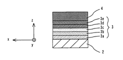


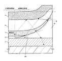


Classifications
-
- H—ELECTRICITY
- H05—ELECTRIC TECHNIQUES NOT OTHERWISE PROVIDED FOR
- H05B—ELECTRIC HEATING; ELECTRIC LIGHT SOURCES NOT OTHERWISE PROVIDED FOR; CIRCUIT ARRANGEMENTS FOR ELECTRIC LIGHT SOURCES, IN GENERAL
- H05B33/00—Electroluminescent light sources
- H05B33/12—Light sources with substantially two-dimensional [2D] radiating surfaces
- H05B33/26—Light sources with substantially two-dimensional [2D] radiating surfaces characterised by the composition or arrangement of the conductive material used as an electrode
- H05B33/28—Light sources with substantially two-dimensional [2D] radiating surfaces characterised by the composition or arrangement of the conductive material used as an electrode of translucent electrodes
-
- H—ELECTRICITY
- H10—SEMICONDUCTOR DEVICES; ELECTRIC SOLID-STATE DEVICES NOT OTHERWISE PROVIDED FOR
- H10K—ORGANIC ELECTRIC SOLID-STATE DEVICES
- H10K50/00—Organic light-emitting devices
- H10K50/80—Constructional details
- H10K50/805—Electrodes
- H10K50/81—Anodes
- H10K50/816—Multilayers, e.g. transparent multilayers
-
- H—ELECTRICITY
- H10—SEMICONDUCTOR DEVICES; ELECTRIC SOLID-STATE DEVICES NOT OTHERWISE PROVIDED FOR
- H10K—ORGANIC ELECTRIC SOLID-STATE DEVICES
- H10K50/00—Organic light-emitting devices
- H10K50/80—Constructional details
- H10K50/805—Electrodes
- H10K50/82—Cathodes
-
- H—ELECTRICITY
- H10—SEMICONDUCTOR DEVICES; ELECTRIC SOLID-STATE DEVICES NOT OTHERWISE PROVIDED FOR
- H10K—ORGANIC ELECTRIC SOLID-STATE DEVICES
- H10K50/00—Organic light-emitting devices
- H10K50/80—Constructional details
- H10K50/85—Arrangements for extracting light from the devices
- H10K50/858—Arrangements for extracting light from the devices comprising refractive means, e.g. lenses
-
- H—ELECTRICITY
- H10—SEMICONDUCTOR DEVICES; ELECTRIC SOLID-STATE DEVICES NOT OTHERWISE PROVIDED FOR
- H10K—ORGANIC ELECTRIC SOLID-STATE DEVICES
- H10K59/00—Integrated devices, or assemblies of multiple devices, comprising at least one organic light-emitting element covered by group H10K50/00
- H10K59/10—OLED displays
- H10K59/12—Active-matrix OLED [AMOLED] displays
- H10K59/122—Pixel-defining structures or layers, e.g. banks
-
- H—ELECTRICITY
- H10—SEMICONDUCTOR DEVICES; ELECTRIC SOLID-STATE DEVICES NOT OTHERWISE PROVIDED FOR
- H10K—ORGANIC ELECTRIC SOLID-STATE DEVICES
- H10K59/00—Integrated devices, or assemblies of multiple devices, comprising at least one organic light-emitting element covered by group H10K50/00
- H10K59/10—OLED displays
- H10K59/17—Passive-matrix OLED displays
- H10K59/173—Passive-matrix OLED displays comprising banks or shadow masks
-
- H—ELECTRICITY
- H10—SEMICONDUCTOR DEVICES; ELECTRIC SOLID-STATE DEVICES NOT OTHERWISE PROVIDED FOR
- H10K—ORGANIC ELECTRIC SOLID-STATE DEVICES
- H10K59/00—Integrated devices, or assemblies of multiple devices, comprising at least one organic light-emitting element covered by group H10K50/00
- H10K59/80—Constructional details
- H10K59/805—Electrodes
- H10K59/8052—Cathodes
-
- H—ELECTRICITY
- H10—SEMICONDUCTOR DEVICES; ELECTRIC SOLID-STATE DEVICES NOT OTHERWISE PROVIDED FOR
- H10K—ORGANIC ELECTRIC SOLID-STATE DEVICES
- H10K59/00—Integrated devices, or assemblies of multiple devices, comprising at least one organic light-emitting element covered by group H10K50/00
- H10K59/80—Constructional details
- H10K59/875—Arrangements for extracting light from the devices
- H10K59/879—Arrangements for extracting light from the devices comprising refractive means, e.g. lenses
-
- H—ELECTRICITY
- H10—SEMICONDUCTOR DEVICES; ELECTRIC SOLID-STATE DEVICES NOT OTHERWISE PROVIDED FOR
- H10K—ORGANIC ELECTRIC SOLID-STATE DEVICES
- H10K77/00—Constructional details of devices covered by this subclass and not covered by groups H10K10/80, H10K30/80, H10K50/80 or H10K59/80
- H10K77/10—Substrates, e.g. flexible substrates
-
- H—ELECTRICITY
- H10—SEMICONDUCTOR DEVICES; ELECTRIC SOLID-STATE DEVICES NOT OTHERWISE PROVIDED FOR
- H10K—ORGANIC ELECTRIC SOLID-STATE DEVICES
- H10K59/00—Integrated devices, or assemblies of multiple devices, comprising at least one organic light-emitting element covered by group H10K50/00
- H10K59/80—Constructional details
- H10K59/805—Electrodes
- H10K59/8051—Anodes
- H10K59/80517—Multilayers, e.g. transparent multilayers
-
- Y—GENERAL TAGGING OF NEW TECHNOLOGICAL DEVELOPMENTS; GENERAL TAGGING OF CROSS-SECTIONAL TECHNOLOGIES SPANNING OVER SEVERAL SECTIONS OF THE IPC; TECHNICAL SUBJECTS COVERED BY FORMER USPC CROSS-REFERENCE ART COLLECTIONS [XRACs] AND DIGESTS
- Y02—TECHNOLOGIES OR APPLICATIONS FOR MITIGATION OR ADAPTATION AGAINST CLIMATE CHANGE
- Y02E—REDUCTION OF GREENHOUSE GAS [GHG] EMISSIONS, RELATED TO ENERGY GENERATION, TRANSMISSION OR DISTRIBUTION
- Y02E10/00—Energy generation through renewable energy sources
- Y02E10/50—Photovoltaic [PV] energy
- Y02E10/549—Organic PV cells
Landscapes
- Physics & Mathematics (AREA)
- Optics & Photonics (AREA)
- Engineering & Computer Science (AREA)
- Microelectronics & Electronic Packaging (AREA)
- Electroluminescent Light Sources (AREA)
Applications Claiming Priority (1)
| Application Number | Priority Date | Filing Date | Title |
|---|---|---|---|
| PCT/JP2012/065749 WO2013190661A1 (fr) | 2012-06-20 | 2012-06-20 | Dispositif électroluminescent organique |
Publications (2)
| Publication Number | Publication Date |
|---|---|
| JPWO2013190661A1 JPWO2013190661A1 (ja) | 2016-02-08 |
| JP6074423B2 true JP6074423B2 (ja) | 2017-02-01 |
Family
ID=49768290
Family Applications (1)
| Application Number | Title | Priority Date | Filing Date |
|---|---|---|---|
| JP2014521149A Active JP6074423B2 (ja) | 2012-06-20 | 2012-06-20 | 有機エレクトロルミネッセンスデバイス |
Country Status (5)
| Country | Link |
|---|---|
| US (1) | US20150206927A1 (fr) |
| EP (1) | EP2852256A4 (fr) |
| JP (1) | JP6074423B2 (fr) |
| CN (1) | CN104396345B (fr) |
| WO (1) | WO2013190661A1 (fr) |
Cited By (1)
| Publication number | Priority date | Publication date | Assignee | Title |
|---|---|---|---|---|
| KR20190130106A (ko) * | 2018-05-11 | 2019-11-21 | 삼성디스플레이 주식회사 | 디스플레이 장치 |
Families Citing this family (20)
| Publication number | Priority date | Publication date | Assignee | Title |
|---|---|---|---|---|
| CN104167431B (zh) * | 2014-08-12 | 2018-05-25 | 京东方科技集团股份有限公司 | Oled显示器件及应用其的oled显示装置 |
| JP6492713B2 (ja) * | 2015-02-05 | 2019-04-03 | 王子ホールディングス株式会社 | El表示装置 |
| CN104795429B (zh) * | 2015-04-13 | 2017-09-01 | 深圳市华星光电技术有限公司 | Oled显示器件 |
| CN104779268B (zh) * | 2015-04-13 | 2016-07-06 | 深圳市华星光电技术有限公司 | Oled显示器件 |
| US20180197927A1 (en) * | 2015-06-12 | 2018-07-12 | Merck Patent Gmbh | Organic electronic devices with fluoropolymer bank structures |
| JP2017181831A (ja) | 2016-03-31 | 2017-10-05 | ソニー株式会社 | 表示装置及び電子機器 |
| KR101695652B1 (ko) * | 2016-04-11 | 2017-01-12 | 엘지디스플레이 주식회사 | 유기발광표시장치와 그의 제조방법 |
| JP2022016557A (ja) * | 2017-02-27 | 2022-01-21 | パイオニア株式会社 | 発光装置 |
| WO2018179133A1 (fr) * | 2017-03-29 | 2018-10-04 | シャープ株式会社 | Dispositif d'affichage, procédé et appareil de production de dispositif d'affichage, appareil de dépôt et dispositif de commande |
| CN107863449A (zh) * | 2017-10-26 | 2018-03-30 | 京东方科技集团股份有限公司 | 一种有机电致发光器件、其制备方法以及显示装置 |
| CN110323249B (zh) * | 2018-03-30 | 2021-10-01 | 上海和辉光电股份有限公司 | 一种有机电致发光显示器件 |
| KR102588082B1 (ko) | 2018-09-06 | 2023-10-11 | 엘지디스플레이 주식회사 | 유기발광표시장치 및 이의 제조 방법 |
| JP7348075B2 (ja) | 2018-11-20 | 2023-09-20 | 京東方科技集團股▲ふん▼有限公司 | 画素構造、表示装置及び画素構造の製造方法 |
| KR102075728B1 (ko) | 2018-12-17 | 2020-02-10 | 엘지디스플레이 주식회사 | 표시패널 |
| KR102922926B1 (ko) * | 2019-05-23 | 2026-02-03 | 엘지디스플레이 주식회사 | 발광 표시 장치 |
| JP6804591B2 (ja) * | 2019-06-13 | 2020-12-23 | 株式会社Joled | 表示装置 |
| CN114639793A (zh) * | 2020-12-16 | 2022-06-17 | 京东方科技集团股份有限公司 | 显示基板及其制备方法、显示装置 |
| CN113130616B (zh) * | 2021-04-20 | 2022-08-23 | 湖北长江新型显示产业创新中心有限公司 | 一种显示面板及显示装置 |
| CN113314573B (zh) * | 2021-05-24 | 2023-05-12 | 武汉华星光电半导体显示技术有限公司 | 显示面板及电子设备 |
| CN119277894B (zh) * | 2024-11-15 | 2025-12-16 | 合肥维信诺科技有限公司 | 显示面板及显示装置 |
Family Cites Families (26)
| Publication number | Priority date | Publication date | Assignee | Title |
|---|---|---|---|---|
| JP2002164181A (ja) * | 2000-09-18 | 2002-06-07 | Semiconductor Energy Lab Co Ltd | 表示装置及びその作製方法 |
| US6739931B2 (en) * | 2000-09-18 | 2004-05-25 | Semiconductor Energy Laboratory Co., Ltd. | Display device and method of fabricating the display device |
| JP4801278B2 (ja) * | 2001-04-23 | 2011-10-26 | 株式会社半導体エネルギー研究所 | 発光装置及びその作製方法 |
| TWI224880B (en) * | 2002-07-25 | 2004-12-01 | Sanyo Electric Co | Organic electroluminescence display device |
| KR100908234B1 (ko) * | 2003-02-13 | 2009-07-20 | 삼성모바일디스플레이주식회사 | 전계 발광 표시 장치 및 이의 제조방법 |
| JP4049033B2 (ja) * | 2003-06-26 | 2008-02-20 | セイコーエプソン株式会社 | 有機el装置とその製造方法 |
| JP4522760B2 (ja) * | 2003-06-30 | 2010-08-11 | 株式会社半導体エネルギー研究所 | 発光装置及び発光装置の作製方法 |
| JP3915806B2 (ja) * | 2003-11-11 | 2007-05-16 | セイコーエプソン株式会社 | 電気光学装置および電子機器 |
| CN100364135C (zh) * | 2003-11-19 | 2008-01-23 | 友达光电股份有限公司 | 高亮度有机发光显示面板的像素结构 |
| JP2005310591A (ja) * | 2004-04-22 | 2005-11-04 | Seiko Epson Corp | 有機el表示装置とその製造方法、並びに電子機器 |
| JP2005340011A (ja) * | 2004-05-27 | 2005-12-08 | Seiko Epson Corp | 電気光学装置及び電子機器 |
| JP2006004743A (ja) * | 2004-06-17 | 2006-01-05 | Toshiba Matsushita Display Technology Co Ltd | 表示装置及びその製造方法 |
| US7554265B2 (en) * | 2004-06-25 | 2009-06-30 | Semiconductor Energy Laboratory Co., Ltd. | Display device |
| JP2006038987A (ja) * | 2004-07-23 | 2006-02-09 | Seiko Epson Corp | 表示装置、表示装置の製造方法、電子機器 |
| JP5587174B2 (ja) * | 2007-04-17 | 2014-09-10 | コーニンクレッカ フィリップス エヌ ヴェ | 織物発光装置 |
| JP4280301B2 (ja) * | 2007-05-31 | 2009-06-17 | パナソニック株式会社 | 有機el素子、およびその製造方法 |
| WO2009075075A1 (fr) * | 2007-12-10 | 2009-06-18 | Panasonic Corporation | Dispositif électroluminescent organique, panneau d'affichage électroluminescent, procédé de fabrication du dispositif électroluminescent organique et procédé de fabrication du panneau d'affichage électroluminescent |
| JP5245448B2 (ja) * | 2008-02-22 | 2013-07-24 | カシオ計算機株式会社 | 有機エレクトロルミネセンス表示装置及びその製造方法 |
| JP5199773B2 (ja) * | 2008-07-30 | 2013-05-15 | 住友化学株式会社 | 有機エレクトロルミネッセンス素子およびその製造方法 |
| JP4884452B2 (ja) * | 2008-12-09 | 2012-02-29 | 三洋電機株式会社 | 有機電界発光パネルの製造方法 |
| JP2010182449A (ja) * | 2009-02-03 | 2010-08-19 | Fujifilm Corp | 有機el表示装置 |
| KR20110049578A (ko) * | 2009-11-05 | 2011-05-12 | 삼성모바일디스플레이주식회사 | 유기 전계 발광 표시장치 |
| JP2011154809A (ja) * | 2010-01-26 | 2011-08-11 | Osaka Prefecture Univ | 有機el素子及びその製造方法 |
| KR101084193B1 (ko) * | 2010-02-16 | 2011-11-17 | 삼성모바일디스플레이주식회사 | 유기 발광 표시 장치 및 그 제조방법 |
| JP2012028226A (ja) * | 2010-07-26 | 2012-02-09 | Dainippon Printing Co Ltd | 有機エレクトロルミネッセンスパネルおよび有機エレクトロルミネッセンス装置 |
| CN103050641B (zh) * | 2011-10-14 | 2016-03-02 | 乐金显示有限公司 | 有机发光器件和使用该器件的显示板 |
-
2012
- 2012-06-20 EP EP12879516.8A patent/EP2852256A4/fr not_active Withdrawn
- 2012-06-20 JP JP2014521149A patent/JP6074423B2/ja active Active
- 2012-06-20 US US14/408,469 patent/US20150206927A1/en not_active Abandoned
- 2012-06-20 CN CN201280074166.7A patent/CN104396345B/zh active Active
- 2012-06-20 WO PCT/JP2012/065749 patent/WO2013190661A1/fr not_active Ceased
Cited By (2)
| Publication number | Priority date | Publication date | Assignee | Title |
|---|---|---|---|---|
| KR20190130106A (ko) * | 2018-05-11 | 2019-11-21 | 삼성디스플레이 주식회사 | 디스플레이 장치 |
| KR102615115B1 (ko) * | 2018-05-11 | 2023-12-19 | 삼성디스플레이 주식회사 | 디스플레이 장치 |
Also Published As
| Publication number | Publication date |
|---|---|
| US20150206927A1 (en) | 2015-07-23 |
| CN104396345B (zh) | 2016-08-24 |
| EP2852256A1 (fr) | 2015-03-25 |
| EP2852256A4 (fr) | 2016-04-27 |
| WO2013190661A1 (fr) | 2013-12-27 |
| JPWO2013190661A1 (ja) | 2016-02-08 |
| CN104396345A (zh) | 2015-03-04 |
Similar Documents
| Publication | Publication Date | Title |
|---|---|---|
| JP6074423B2 (ja) | 有機エレクトロルミネッセンスデバイス | |
| KR101988217B1 (ko) | 유기 발광 다이오드 마이크로-캐비티 구조 및 그 제조 방법 | |
| US7282856B2 (en) | Electroluminescent display having an adhesive layer comprised of two or more liquids | |
| JP4534054B2 (ja) | 有機el表示パネルとその製法 | |
| JP6688701B2 (ja) | 有機el表示パネル、及び有機el表示パネルの製造方法 | |
| JP2017054601A (ja) | 有機el素子、それを用いた有機el表示パネル、及び有機el表示パネルの製造方法 | |
| CN109216407B (zh) | Oled显示面板及其制备方法 | |
| JP2005327674A (ja) | 有機エレクトロルミネッセント表示素子、それを有する表示装置、及び、その製造方法 | |
| JP6168610B2 (ja) | 有機el照明パネル用基板、有機el照明パネルおよび有機el照明装置 | |
| US20140027735A1 (en) | Organic light emitting diode display and manufacturing method thereof | |
| KR20210012415A (ko) | 발광 표시 장치 | |
| US9082736B2 (en) | Organic EL panel and method of manufacturing the same | |
| WO2013186919A1 (fr) | Dispositif électroluminescent organique | |
| US9653707B2 (en) | Organic light emitting diode display | |
| WO2013186916A1 (fr) | Dispositif électroluminescent organique | |
| KR100822959B1 (ko) | 반사 측벽을 가지는 유기전계발광장치 및 이의 제조 방법. | |
| JP2005183048A (ja) | 発光素子基板およびそれを用いた発光素子 | |
| WO2013161000A1 (fr) | Elément émetteur de lumière et procédé de fabrication | |
| WO2013186917A1 (fr) | Dispositif électroluminescent organique | |
| WO2013186918A1 (fr) | Dispositif électroluminescent organique | |
| KR102075787B1 (ko) | 유기 발광 표시 장치 및 그 제조방법 | |
| JP2010033985A (ja) | 多色発光表示装置 | |
| JP2000003793A (ja) | 電界発光素子 | |
| WO2013190621A1 (fr) | Élément électroluminescent | |
| WO2014013567A1 (fr) | Élément luminescent |
Legal Events
| Date | Code | Title | Description |
|---|---|---|---|
| A131 | Notification of reasons for refusal |
Free format text: JAPANESE INTERMEDIATE CODE: A131 Effective date: 20151215 |
|
| A521 | Request for written amendment filed |
Free format text: JAPANESE INTERMEDIATE CODE: A523 Effective date: 20160210 |
|
| A02 | Decision of refusal |
Free format text: JAPANESE INTERMEDIATE CODE: A02 Effective date: 20160802 |
|
| A521 | Request for written amendment filed |
Free format text: JAPANESE INTERMEDIATE CODE: A523 Effective date: 20161018 |
|
| A911 | Transfer to examiner for re-examination before appeal (zenchi) |
Free format text: JAPANESE INTERMEDIATE CODE: A911 Effective date: 20161026 |
|
| TRDD | Decision of grant or rejection written | ||
| A01 | Written decision to grant a patent or to grant a registration (utility model) |
Free format text: JAPANESE INTERMEDIATE CODE: A01 Effective date: 20161220 |
|
| A61 | First payment of annual fees (during grant procedure) |
Free format text: JAPANESE INTERMEDIATE CODE: A61 Effective date: 20170106 |
|
| R150 | Certificate of patent or registration of utility model |
Ref document number: 6074423 Country of ref document: JP Free format text: JAPANESE INTERMEDIATE CODE: R150 |