WO2013190661A1 - Dispositif électroluminescent organique - Google Patents
Dispositif électroluminescent organique Download PDFInfo
- Publication number
- WO2013190661A1 WO2013190661A1 PCT/JP2012/065749 JP2012065749W WO2013190661A1 WO 2013190661 A1 WO2013190661 A1 WO 2013190661A1 JP 2012065749 W JP2012065749 W JP 2012065749W WO 2013190661 A1 WO2013190661 A1 WO 2013190661A1
- Authority
- WO
- WIPO (PCT)
- Prior art keywords
- organic
- bank
- layer
- light emitting
- light
- Prior art date
- Legal status (The legal status is an assumption and is not a legal conclusion. Google has not performed a legal analysis and makes no representation as to the accuracy of the status listed.)
- Ceased
Links
Images





Classifications
-
- H—ELECTRICITY
- H05—ELECTRIC TECHNIQUES NOT OTHERWISE PROVIDED FOR
- H05B—ELECTRIC HEATING; ELECTRIC LIGHT SOURCES NOT OTHERWISE PROVIDED FOR; CIRCUIT ARRANGEMENTS FOR ELECTRIC LIGHT SOURCES, IN GENERAL
- H05B33/00—Electroluminescent light sources
- H05B33/12—Light sources with substantially two-dimensional [2D] radiating surfaces
- H05B33/26—Light sources with substantially two-dimensional [2D] radiating surfaces characterised by the composition or arrangement of the conductive material used as an electrode
- H05B33/28—Light sources with substantially two-dimensional [2D] radiating surfaces characterised by the composition or arrangement of the conductive material used as an electrode of translucent electrodes
-
- H—ELECTRICITY
- H10—SEMICONDUCTOR DEVICES; ELECTRIC SOLID-STATE DEVICES NOT OTHERWISE PROVIDED FOR
- H10K—ORGANIC ELECTRIC SOLID-STATE DEVICES
- H10K50/00—Organic light-emitting devices
- H10K50/80—Constructional details
- H10K50/805—Electrodes
- H10K50/81—Anodes
- H10K50/816—Multilayers, e.g. transparent multilayers
-
- H—ELECTRICITY
- H10—SEMICONDUCTOR DEVICES; ELECTRIC SOLID-STATE DEVICES NOT OTHERWISE PROVIDED FOR
- H10K—ORGANIC ELECTRIC SOLID-STATE DEVICES
- H10K50/00—Organic light-emitting devices
- H10K50/80—Constructional details
- H10K50/805—Electrodes
- H10K50/82—Cathodes
-
- H—ELECTRICITY
- H10—SEMICONDUCTOR DEVICES; ELECTRIC SOLID-STATE DEVICES NOT OTHERWISE PROVIDED FOR
- H10K—ORGANIC ELECTRIC SOLID-STATE DEVICES
- H10K50/00—Organic light-emitting devices
- H10K50/80—Constructional details
- H10K50/85—Arrangements for extracting light from the devices
- H10K50/858—Arrangements for extracting light from the devices comprising refractive means, e.g. lenses
-
- H—ELECTRICITY
- H10—SEMICONDUCTOR DEVICES; ELECTRIC SOLID-STATE DEVICES NOT OTHERWISE PROVIDED FOR
- H10K—ORGANIC ELECTRIC SOLID-STATE DEVICES
- H10K59/00—Integrated devices, or assemblies of multiple devices, comprising at least one organic light-emitting element covered by group H10K50/00
- H10K59/10—OLED displays
- H10K59/12—Active-matrix OLED [AMOLED] displays
- H10K59/122—Pixel-defining structures or layers, e.g. banks
-
- H—ELECTRICITY
- H10—SEMICONDUCTOR DEVICES; ELECTRIC SOLID-STATE DEVICES NOT OTHERWISE PROVIDED FOR
- H10K—ORGANIC ELECTRIC SOLID-STATE DEVICES
- H10K59/00—Integrated devices, or assemblies of multiple devices, comprising at least one organic light-emitting element covered by group H10K50/00
- H10K59/10—OLED displays
- H10K59/17—Passive-matrix OLED displays
- H10K59/173—Passive-matrix OLED displays comprising banks or shadow masks
-
- H—ELECTRICITY
- H10—SEMICONDUCTOR DEVICES; ELECTRIC SOLID-STATE DEVICES NOT OTHERWISE PROVIDED FOR
- H10K—ORGANIC ELECTRIC SOLID-STATE DEVICES
- H10K59/00—Integrated devices, or assemblies of multiple devices, comprising at least one organic light-emitting element covered by group H10K50/00
- H10K59/80—Constructional details
- H10K59/805—Electrodes
- H10K59/8052—Cathodes
-
- H—ELECTRICITY
- H10—SEMICONDUCTOR DEVICES; ELECTRIC SOLID-STATE DEVICES NOT OTHERWISE PROVIDED FOR
- H10K—ORGANIC ELECTRIC SOLID-STATE DEVICES
- H10K59/00—Integrated devices, or assemblies of multiple devices, comprising at least one organic light-emitting element covered by group H10K50/00
- H10K59/80—Constructional details
- H10K59/875—Arrangements for extracting light from the devices
- H10K59/879—Arrangements for extracting light from the devices comprising refractive means, e.g. lenses
-
- H—ELECTRICITY
- H10—SEMICONDUCTOR DEVICES; ELECTRIC SOLID-STATE DEVICES NOT OTHERWISE PROVIDED FOR
- H10K—ORGANIC ELECTRIC SOLID-STATE DEVICES
- H10K77/00—Constructional details of devices covered by this subclass and not covered by groups H10K10/80, H10K30/80, H10K50/80 or H10K59/80
- H10K77/10—Substrates, e.g. flexible substrates
-
- H—ELECTRICITY
- H10—SEMICONDUCTOR DEVICES; ELECTRIC SOLID-STATE DEVICES NOT OTHERWISE PROVIDED FOR
- H10K—ORGANIC ELECTRIC SOLID-STATE DEVICES
- H10K59/00—Integrated devices, or assemblies of multiple devices, comprising at least one organic light-emitting element covered by group H10K50/00
- H10K59/80—Constructional details
- H10K59/805—Electrodes
- H10K59/8051—Anodes
- H10K59/80517—Multilayers, e.g. transparent multilayers
-
- Y—GENERAL TAGGING OF NEW TECHNOLOGICAL DEVELOPMENTS; GENERAL TAGGING OF CROSS-SECTIONAL TECHNOLOGIES SPANNING OVER SEVERAL SECTIONS OF THE IPC; TECHNICAL SUBJECTS COVERED BY FORMER USPC CROSS-REFERENCE ART COLLECTIONS [XRACs] AND DIGESTS
- Y02—TECHNOLOGIES OR APPLICATIONS FOR MITIGATION OR ADAPTATION AGAINST CLIMATE CHANGE
- Y02E—REDUCTION OF GREENHOUSE GAS [GHG] EMISSIONS, RELATED TO ENERGY GENERATION, TRANSMISSION OR DISTRIBUTION
- Y02E10/00—Energy generation through renewable energy sources
- Y02E10/50—Photovoltaic [PV] energy
- Y02E10/549—Organic PV cells
Definitions
- the present invention relates to an organic electroluminescence device (hereinafter referred to as an organic EL device) including at least one organic electroluminescence element.
- the organic electroluminescence element is configured by, for example, sequentially laminating an organic layer including an anode, a light emitting layer, and a cathode on a transparent glass substrate, and electroluminescence (hereinafter, referred to as “electroluminescence” by injecting current into the organic layer through the anode and the cathode).
- EL element electroluminescence
- the emitted light from the light emitting layer is taken out through the transparent electrode and the substrate by making the electrode on the substrate side transparent.
- about 20% of the light emitted from the light emitting layer is about 20%. Only light can be taken out.
- a bank that partitions an organic layer on a transparent substrate on the light extraction side is made of a transparent material, and a reflection unit that extracts light propagating in the light-transmitting bank to the transparent substrate side in the viewing direction. It discloses a technology that is provided to increase the light extraction efficiency.
- Patent Document 1 Although light from the light emitting layer in contact with the side surface of the light-transmitting bank is extracted to the bank, there is a problem that light propagating in the organic layer before being extracted to the bank is attenuated.
- the organic EL device of the present invention is an organic EL device having a translucent substrate and at least one organic EL element carried on the translucent substrate,
- the organic EL element includes at least one insulating bank disposed on the translucent substrate, a translucent electrode in contact with the bank, and an organic layer including a light emitting layer formed on the translucent electrode.
- the bank is made of a translucent dielectric material having a low refractive index equal to or lower than the refractive index of the organic layer,
- the bank has a side surface of an inclined surface that is inclined with respect to the light-transmitting substrate, and the light emitting layer extends across an inclined surface that is separated from the inclined surface that is in contact with the light emitting layer and is in contact with the portion of the organic layer that is in contact with the reflective electrode. It has a concave shape facing the surface.
- FIG. 1 is a plan view of an organic EL device according to an embodiment of the present invention.
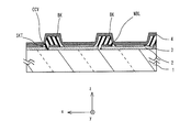
- FIG. 2 is a sectional view taken along the line CC in FIG.
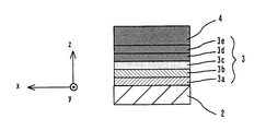
- FIG. 3 is a schematic cross-sectional view schematically showing a laminated structure of the light emitting portion of the organic EL device shown in FIG.
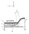
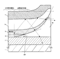
- FIG. 4 is an enlarged partial sectional view showing a part of the organic EL device shown in FIG.
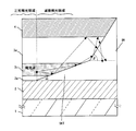
- FIG. 5 is an enlarged partial sectional view showing a part of an organic EL device according to another embodiment of the present invention.
- FIG. 6 is an enlarged partial sectional view showing a part of an organic EL device according to one modification.
- FIG. 7 is an enlarged partial cross-sectional view showing a part of another modified organic EL device.
- FIG. 1 is a plan view of an organic EL device according to an embodiment of the present invention.
- FIG. 2 is a sectional view taken along the line CC in FIG.
- FIG. 3 is a schematic cross-sectional view
- FIG. 8 is an enlarged partial sectional view showing a part of an organic EL device according to another modification.
- FIG. 9 is an enlarged partial cross-sectional view showing a part of another modified organic EL device.
- FIG. 10 is an enlarged partial cross-sectional view showing a part of another modified organic EL device.
- an organic EL device OELD includes a plurality of strip-shaped organic EL elements OELE which are partitioned by a plurality of banks BK on a light-transmitting flat substrate 1 such as glass or resin and extend in the y direction. Yes.
- the plurality of organic EL elements OELE are juxtaposed with each other, for example, exhibiting different emission colors of red light emission R, green light emission G, and blue light emission B.
- the organic EL elements of RGB emission colors are arranged as a set in the x direction for each set.
- each of the organic EL elements of the organic EL device is configured by laminating a translucent electrode 2, an organic layer 3 including a light emitting layer, and a reflective electrode 4 on a substrate 1 between banks BK.
- the This organic EL device is a so-called bottom emission type organic EL panel that takes out light generated in the organic layer 3 from the surface of the substrate 1 by applying a voltage between the translucent electrode 2 and the reflective electrode 4. .
- the bank BK in contact with the translucent electrode 2 is formed of a translucent dielectric material having a low refractive index equal to or lower than the refractive index of the organic layer 3.
- “equivalent refractive index” means that the difference between one refractive index and the other refractive index is less than 0.3, preferably 0.2 or less, particularly preferably 0.1 or less. That means. Further, the refractive index “low” or “high” may be “low” or “high” to such an extent that a difference in measurement occurs, but in practice, it exceeds 0.1, preferably exceeds 0.2. More preferably 0.3 or more, still more preferably 0.4 or more, particularly preferably 0.5 or more, indicating a low or high difference.
- the plurality of translucent electrodes 2 constituting the anode each have a band shape, extend along the y direction on the substrate 1, and are deposited in parallel with each other in parallel in the x direction at regular intervals.
- a bank BK is formed extending along the y direction so as to cover them.
- the bank BK rectangular openings each extending in the y direction are formed.
- An organic layer 3 is disposed in each of the openings.
- the organic layer 3 is juxtaposed in a state of being separated from each other by the bank BK, and partitions a plurality of light emitting regions separated by the bank BK.
- the bank BK is covered with at least a part of the reflective electrode 4.
- the bank BK includes an organic material bank and an inorganic material bank, and an inorganic material bank is generally formed by etching.
- wet coating methods such as screen printing, spraying method, ink jet method, spin coating method, gravure printing, and roll coater method are known.
- the bank BK in the organic EL device has a side surface of an inclined surface that is inclined with respect to the translucent substrate 2 along the y direction, and the side surface has a concave shape CCV in contact with the organic layer 3. .
- the skirt portion SKT which is a part of the concave shape CCV terminates at the interface between the organic layer 3 and the translucent electrode 2.
- a hole injection layer 3a, a hole transport layer 3b, a light emitting layer 3c, an electron transport layer 3d, and an electron is laminated in order.
- the organic layer 3 sandwiched between the translucent electrode 2 and the reflective electrode 4 is a light emitting laminated body, and is not limited to these laminated structures.
- a hole blocking layer between the light emitting layer 3c and the electron transporting layer 3d (
- a layered structure including at least a light emitting layer or a charge transport layer that can also be used may be used.
- the organic layer 3 may be configured by omitting the hole transport layer 3b, the hole injection layer 3a, or the hole injection layer 3a and the electron transport layer 3d from the stacked structure. May be.
- any known light emitting material such as a fluorescent material or a phosphorescent material can be applied.
- Examples of fluorescent materials that emit blue light include naphthalene, perylene, and pyrene.
- fluorescent materials that give green light emission include quinacridone derivatives, coumarin derivatives, and aluminum complexes such as Alq3 (tris (8-hydroxy-quinoline) aluminum).
- Examples of fluorescent materials that give yellow light include rubrene derivatives.
- Examples of fluorescent materials that give red light emission include DCM (4- (dicyanomethylene) -2-methyl-6- (p-dimethylaminostyryl) -4H-pyran) compounds, benzopyran derivatives, rhodamine derivatives, and the like.
- Examples of the phosphorescent material include iridium, platinum, ruthenium, rhodium, and palladium complex compounds. Specific examples of the phosphorescent material include tris (2-phenylpyridine) iridium (so-called Ir (ppy) 3), tris (2-phenylpyridine) ruthenium, and the like.
- the organic layers 3 that emit red, green, and blue emission colors are repeatedly arranged in parallel, and red, green, and blue light are arbitrarily emitted from the surface of the substrate 1 that serves as a light extraction surface. Light that is mixed in proportion and recognized as a single emission color is emitted.
- Known methods for forming the organic layer 3 include dry coating methods such as sputtering and vacuum deposition, and wet coating methods such as screen printing, spraying, ink jetting, spin coating, gravure printing, and roll coater. ing.
- dry coating methods such as sputtering and vacuum deposition
- wet coating methods such as screen printing, spraying, ink jetting, spin coating, gravure printing, and roll coater.
- the hole injection layer, the hole transport layer, and the light emitting layer are uniformly formed by a wet coating method
- the electron transport layer and the electron injection layer are sequentially formed uniformly by a dry coating method.
- a film may be formed.
- all the functional layers may be sequentially formed in a uniform film thickness by a wet coating method.
- the anode translucent electrode 2 for supplying holes to the functional layers up to the light emitting layer 3c is ITO (Indium-tin-oxide), ZnO, ZnO—Al 2 O 3 (so-called AZO), In 2 O 3 ⁇ It may be composed of ZnO (so-called IZO), SnO 2 —Sb 2 O 3 (so-called ATO), RuO 2 or the like. Furthermore, for the translucent electrode 2, it is preferable to select a material having a transmittance of at least 10% at the emission wavelength obtained from the light emitting layer.
- the translucent electrode 2 usually has a single-layer structure, but it can also have a laminated structure made of a plurality of materials if desired.
- the cathode reflective electrode 4 that supplies electrons to the functional layers up to the light emitting layer 3c is not limited, and for example, metals such as aluminum, silver, copper, nickel, chromium, gold, and platinum are used. In addition, these materials may be used only by 1 type and may use 2 or more types together by arbitrary combinations and a ratio.
- the material of the reflective electrode 4 preferably includes a metal having a low work function in order to efficiently inject electrons.
- a suitable metal such as tin, magnesium, indium, calcium, aluminum, silver, or an alloy thereof may be used. Used. Specific examples include low work function alloy electrodes such as magnesium-silver alloy, magnesium-indium alloy, and aluminum-lithium alloy.
- the silver thin film with a thickness of 20 nm of the reflective electrode 4 has a transmittance of 50%.
- An Al film having a thickness of 10 nm as the metal thin film has a transmittance of 50%.
- the 20 nm-thick MgAg alloy film as the metal thin film has a transmittance of 50%.
- electroconductivity can be ensured if the lower limit of the film thickness is 5 nm.
- the reflective electrode 4 can be formed as a single layer film or a multilayer film on the organic layer 3 by sputtering or vacuum deposition.
- the bank BK in the organic EL device has a side surface of an inclined surface that is inclined with respect to the translucent substrate 2.
- the side surface of the bank BK has a concave shape CCV that faces the light emitting layer 3 c from the slope A in contact with the light emitting layer 3 c to the slope B in contact with the portion of the organic layer 3 in contact with the reflective electrode 4.
- the side surface of the bank BK has an angle ⁇ formed with the transparent substrate 2 of the slope A in contact with the light emitting layer 3 c smaller than the angle ⁇ formed with the transparent substrate 2 of the slope B in contact with the portion of the organic layer 3 in contact with the reflective electrode 4.
- the base portion SKT of the bank BK terminates at the interface between the organic layer 3 and the translucent electrode 2.
- the organic layer 3 on the bank BK side becomes an attenuated light emission region with the end of the bank BK as a boundary, and the organic layer 3 away from the skirt portion SKT of the bank BK becomes a normal light emission region. This is because the translucent electrode 2 is covered by the base portion SKT, and the translucent electrode 2 of the anode and the reflective electrode 4 of the cathode do not face each other through the organic layer 3.
- the light L0 incident on the tapered portion of the edge of the organic layer 3 on the bank BK side is repeatedly reflected in a zigzag manner between the tapered reflective electrode 4 and the side surface of the bank BK (ie, the bottom portion SKT). Since it only enters the outermost edge of the layer 3, the reflected light is extremely reduced and enters only the side surface of the bank BK. As described above, in the present embodiment, reflection is repeated at the tapered portion of the edge of the organic layer 3 having a wedge-shaped cross section and guided to the upper part of the bank BK at the back, and the light L0 is emitted only to the side surface of the bank BK. It is a mechanism.
- FIG. 5 shows an ITO transparent electrode 2, which is an anode, a hole injection layer 3a, a light emitting layer 3c, an electron injection layer 3e, and a metal reflective electrode, which is a cathode, laminated on a glass transparent substrate 1.
- 4 shows a part of the organic EL element in the organic EL device constituted by 4.
- the organic layers up to the light emitting layer 3 are formed by a wet coating method such as an inkjet method, and the electron injection layer 3e and the subsequent layers are formed by a vapor deposition method.
- the organic layer 3 on the bank BK side of the concave shape CCV between the slope A and the slope B of the bank BK can be seen as a part of a cylindrical lens extending in the depth y direction.
- the inclination angle ⁇ of the interface of the light emitting layer 3c and the bank BK is the bank BK ⁇ where the reflective electrode 4 is in contact. Is smaller than the inclination angle.
- the anode translucent electrode 2 and the cathode reflecting electrode 4 are in a normal facing state, and the area away from the bank BK from this light emitting point normally emits light and approaches the bank BK. As the amount of light decreases,
- the slope A portion having the slope angle ⁇ of the base portion SKT gradually becomes thicker from the translucent electrode 2 at the slope angle ⁇ .
- the amount of evanescent light oozes off exponentially and oozes out about the wavelength, but the substantial range is said to be about 150 nm.
- the emitted light is transmitted through the bottom SKT with a thickness of about 25 nm to 30 nm, and at a thickness greater than that, an angle of total reflection appears.
- the light L2 that is totally reflected by the slope A and directly reflected by the reflective electrode 4 also enters the bank BK at the slope B.
- the inclination of the bank BK is changed depending on the position of the organic layer, the inclination angle ⁇ is made smaller than the inclination angle ⁇ , and the light emitting layer 3c is disposed inside the concave shape. Even if it is used, a large amount of light can be put into the translucent bank BK. Besides simply increasing the light extraction efficiency as the concave shape CCV, since the near-field light in the thin film portion of the skirt SKT is used, the light can be applied to the bank BK having a low refractive index compared to a mere steep plane slope. Incidence increases.
- the translucent dielectric material of the bank is not particularly lyophilic. In both cases, little consideration is required regarding the wettability of organic materials. In general, when the bank is laid down, the lyophilicity is increased and the organic material can be easily applied. Therefore, it is not necessary to use a lyophilic material for the bank BK, and the range of selection of the bank material is expanded.
- the bank material include fluorine resins such as fluorinated polyolefin resin, fluorinated polyimide resin, and fluorinated polyacrylic resin.
- the translucent bank BK shown in FIG. 5 has a concave shape CCV in which the slope gradually changes, but the present invention is not limited to this, and as shown in FIG. You may comprise B so that it may be a plane and may have inclination-angle (alpha) and inclination-angle (beta), respectively.
- FIG. 7 is a cross-sectional view showing the periphery of the bank BK by partially cutting away the organic EL device of the modification.
- the components denoted by the same reference numerals as those in the above embodiment are the same as those in the organic EL device in the above embodiment, and thus detailed description thereof is omitted.
- the organic layers up to the light emitting layer 3c are formed by a wet coating method such as an ink jet method, and the electron transport layer and the subsequent layers are formed by a vapor deposition method using a mask, and the electron transport layer and the electron injection are formed.
- An organic layer 3 of an electron transport layer or an electron injection layer is formed up to the vicinity of the top of the bank BK by using a layer having a wide mask opening at the time of layer deposition. Therefore, a portion where the organic layer is not deposited on the top surface of the bank BK, that is, a portion where the reflective electrode 4 is in contact with the bank BK is formed.
- the light repeats total reflection up to the bank slope contacting the portion of the organic layer 3 that is in contact with the reflective electrode 4 on the top surface, and the light reaching the reflective electrode 4 on the top surface is translucent. Can enter the sex bank BK.
- the end of the electron injection layer 3e formed by the wet coating method terminates on the side of the bank BK.
- 9 is a coating type in which all the layers of the organic layer 3 are formed by a wet coating method, the thickness of the light emitting layer 3c is increased, and the thickness of the electron injection layer 3e is decreased.
- all layers of the organic layer 3 are formed by a wet coating method, and the RGB light emission of the electron blocking layer and the light emitting layer 3c between the hole injection layer 3a side and the electron injection layer 3e.
- the non-light emitting area such as the bank BK is totally reflected by the translucent electrode 2 portion of the organic layer 3 by using a translucent low refractive index material.
- the light that has been transmitted enters the side surface portion of the bank BK, changes its refraction angle, and is radiated to the substrate 1 at various radiation angles, so that the light extraction efficiency of the light propagating through the transparent electrode can be enhanced.
- the translucent substrate 1 a quartz or glass plate, a metal plate or a metal foil, a resin substrate that can be bent, a plastic film, a sheet, or the like is used.
- a glass plate or a transparent plate made of a synthetic resin such as polyester, polymethacrylate, polycarbonate, or polysulfone is preferable.
- a synthetic resin substrate it is necessary to pay attention to gas barrier properties. If the gas barrier property of the substrate is too small, the organic EL device may be deteriorated by outside air that has passed through the substrate, which is not preferable. Therefore, a method of securing a gas barrier property by providing a dense silicon oxide film or the like on at least one surface of the synthetic resin substrate is also a preferable method.
- a sealing can for covering and sealing the light emitting portions juxtaposed in a strip shape of the organic EL device and the surrounding banks may be provided.
- a light extraction film (not shown) may be attached to the outer surface of the substrate 1 so as to cover the light emitting portion.
- the organic layer is a light emitting laminate, but the light emitting laminate can also be configured by laminating inorganic material films.
Landscapes
- Physics & Mathematics (AREA)
- Optics & Photonics (AREA)
- Engineering & Computer Science (AREA)
- Microelectronics & Electronic Packaging (AREA)
- Electroluminescent Light Sources (AREA)
Priority Applications (5)
| Application Number | Priority Date | Filing Date | Title |
|---|---|---|---|
| US14/408,469 US20150206927A1 (en) | 2012-06-20 | 2012-06-20 | Organic electroluminescent device |
| JP2014521149A JP6074423B2 (ja) | 2012-06-20 | 2012-06-20 | 有機エレクトロルミネッセンスデバイス |
| CN201280074166.7A CN104396345B (zh) | 2012-06-20 | 2012-06-20 | 有机电致发光器件 |
| PCT/JP2012/065749 WO2013190661A1 (fr) | 2012-06-20 | 2012-06-20 | Dispositif électroluminescent organique |
| EP12879516.8A EP2852256A4 (fr) | 2012-06-20 | 2012-06-20 | Dispositif électroluminescent organique |
Applications Claiming Priority (1)
| Application Number | Priority Date | Filing Date | Title |
|---|---|---|---|
| PCT/JP2012/065749 WO2013190661A1 (fr) | 2012-06-20 | 2012-06-20 | Dispositif électroluminescent organique |
Publications (1)
| Publication Number | Publication Date |
|---|---|
| WO2013190661A1 true WO2013190661A1 (fr) | 2013-12-27 |
Family
ID=49768290
Family Applications (1)
| Application Number | Title | Priority Date | Filing Date |
|---|---|---|---|
| PCT/JP2012/065749 Ceased WO2013190661A1 (fr) | 2012-06-20 | 2012-06-20 | Dispositif électroluminescent organique |
Country Status (5)
| Country | Link |
|---|---|
| US (1) | US20150206927A1 (fr) |
| EP (1) | EP2852256A4 (fr) |
| JP (1) | JP6074423B2 (fr) |
| CN (1) | CN104396345B (fr) |
| WO (1) | WO2013190661A1 (fr) |
Cited By (8)
| Publication number | Priority date | Publication date | Assignee | Title |
|---|---|---|---|---|
| CN104167431A (zh) * | 2014-08-12 | 2014-11-26 | 京东方科技集团股份有限公司 | Oled显示器件及应用其的oled显示装置 |
| JP2016143657A (ja) * | 2015-02-05 | 2016-08-08 | 王子ホールディングス株式会社 | El表示装置 |
| WO2018179133A1 (fr) * | 2017-03-29 | 2018-10-04 | シャープ株式会社 | Dispositif d'affichage, procédé et appareil de production de dispositif d'affichage, appareil de dépôt et dispositif de commande |
| JP2019160807A (ja) * | 2019-06-13 | 2019-09-19 | 株式会社Joled | 表示装置 |
| CN110880560A (zh) * | 2018-09-06 | 2020-03-13 | 乐金显示有限公司 | 有机发光显示装置及其制造方法 |
| US10943963B2 (en) | 2018-05-11 | 2021-03-09 | Samsung Display Co., Ltd. | Display device |
| JP2022016557A (ja) * | 2017-02-27 | 2022-01-21 | パイオニア株式会社 | 発光装置 |
| EP3232488B1 (fr) * | 2016-04-11 | 2024-10-30 | LG Display Co., Ltd. | Afficheur et son procédé de fabrication |
Families Citing this family (13)
| Publication number | Priority date | Publication date | Assignee | Title |
|---|---|---|---|---|
| CN104795429B (zh) * | 2015-04-13 | 2017-09-01 | 深圳市华星光电技术有限公司 | Oled显示器件 |
| CN104779268B (zh) * | 2015-04-13 | 2016-07-06 | 深圳市华星光电技术有限公司 | Oled显示器件 |
| US20180197927A1 (en) * | 2015-06-12 | 2018-07-12 | Merck Patent Gmbh | Organic electronic devices with fluoropolymer bank structures |
| JP2017181831A (ja) | 2016-03-31 | 2017-10-05 | ソニー株式会社 | 表示装置及び電子機器 |
| CN107863449A (zh) * | 2017-10-26 | 2018-03-30 | 京东方科技集团股份有限公司 | 一种有机电致发光器件、其制备方法以及显示装置 |
| CN110323249B (zh) * | 2018-03-30 | 2021-10-01 | 上海和辉光电股份有限公司 | 一种有机电致发光显示器件 |
| JP7348075B2 (ja) | 2018-11-20 | 2023-09-20 | 京東方科技集團股▲ふん▼有限公司 | 画素構造、表示装置及び画素構造の製造方法 |
| KR102075728B1 (ko) | 2018-12-17 | 2020-02-10 | 엘지디스플레이 주식회사 | 표시패널 |
| KR102922926B1 (ko) * | 2019-05-23 | 2026-02-03 | 엘지디스플레이 주식회사 | 발광 표시 장치 |
| CN114639793A (zh) * | 2020-12-16 | 2022-06-17 | 京东方科技集团股份有限公司 | 显示基板及其制备方法、显示装置 |
| CN113130616B (zh) * | 2021-04-20 | 2022-08-23 | 湖北长江新型显示产业创新中心有限公司 | 一种显示面板及显示装置 |
| CN113314573B (zh) * | 2021-05-24 | 2023-05-12 | 武汉华星光电半导体显示技术有限公司 | 显示面板及电子设备 |
| CN119277894B (zh) * | 2024-11-15 | 2025-12-16 | 合肥维信诺科技有限公司 | 显示面板及显示装置 |
Citations (10)
| Publication number | Priority date | Publication date | Assignee | Title |
|---|---|---|---|---|
| JP2002164181A (ja) * | 2000-09-18 | 2002-06-07 | Semiconductor Energy Lab Co Ltd | 表示装置及びその作製方法 |
| JP2005310591A (ja) | 2004-04-22 | 2005-11-04 | Seiko Epson Corp | 有機el表示装置とその製造方法、並びに電子機器 |
| JP2006004743A (ja) * | 2004-06-17 | 2006-01-05 | Toshiba Matsushita Display Technology Co Ltd | 表示装置及びその製造方法 |
| WO2008149498A1 (fr) * | 2007-05-31 | 2008-12-11 | Panasonic Corporation | Dispositif électroluminescent organique et procédé de fabrication correspondant |
| JP2009054603A (ja) * | 2008-12-09 | 2009-03-12 | Sanyo Electric Co Ltd | 有機電界発光パネルの製造方法 |
| JP2009198853A (ja) * | 2008-02-22 | 2009-09-03 | Casio Comput Co Ltd | 有機エレクトロルミネセンス表示装置及びその製造方法 |
| JP2010033972A (ja) * | 2008-07-30 | 2010-02-12 | Sumitomo Chemical Co Ltd | 有機エレクトロルミネッセンス素子およびその製造方法 |
| JP2011154809A (ja) * | 2010-01-26 | 2011-08-11 | Osaka Prefecture Univ | 有機el素子及びその製造方法 |
| JP2011171268A (ja) * | 2010-02-16 | 2011-09-01 | Samsung Mobile Display Co Ltd | 有機発光表示装置及びその製造方法 |
| JP2012028226A (ja) * | 2010-07-26 | 2012-02-09 | Dainippon Printing Co Ltd | 有機エレクトロルミネッセンスパネルおよび有機エレクトロルミネッセンス装置 |
Family Cites Families (16)
| Publication number | Priority date | Publication date | Assignee | Title |
|---|---|---|---|---|
| US6739931B2 (en) * | 2000-09-18 | 2004-05-25 | Semiconductor Energy Laboratory Co., Ltd. | Display device and method of fabricating the display device |
| JP4801278B2 (ja) * | 2001-04-23 | 2011-10-26 | 株式会社半導体エネルギー研究所 | 発光装置及びその作製方法 |
| TWI224880B (en) * | 2002-07-25 | 2004-12-01 | Sanyo Electric Co | Organic electroluminescence display device |
| KR100908234B1 (ko) * | 2003-02-13 | 2009-07-20 | 삼성모바일디스플레이주식회사 | 전계 발광 표시 장치 및 이의 제조방법 |
| JP4049033B2 (ja) * | 2003-06-26 | 2008-02-20 | セイコーエプソン株式会社 | 有機el装置とその製造方法 |
| JP4522760B2 (ja) * | 2003-06-30 | 2010-08-11 | 株式会社半導体エネルギー研究所 | 発光装置及び発光装置の作製方法 |
| JP3915806B2 (ja) * | 2003-11-11 | 2007-05-16 | セイコーエプソン株式会社 | 電気光学装置および電子機器 |
| CN100364135C (zh) * | 2003-11-19 | 2008-01-23 | 友达光电股份有限公司 | 高亮度有机发光显示面板的像素结构 |
| JP2005340011A (ja) * | 2004-05-27 | 2005-12-08 | Seiko Epson Corp | 電気光学装置及び電子機器 |
| US7554265B2 (en) * | 2004-06-25 | 2009-06-30 | Semiconductor Energy Laboratory Co., Ltd. | Display device |
| JP2006038987A (ja) * | 2004-07-23 | 2006-02-09 | Seiko Epson Corp | 表示装置、表示装置の製造方法、電子機器 |
| JP5587174B2 (ja) * | 2007-04-17 | 2014-09-10 | コーニンクレッカ フィリップス エヌ ヴェ | 織物発光装置 |
| WO2009075075A1 (fr) * | 2007-12-10 | 2009-06-18 | Panasonic Corporation | Dispositif électroluminescent organique, panneau d'affichage électroluminescent, procédé de fabrication du dispositif électroluminescent organique et procédé de fabrication du panneau d'affichage électroluminescent |
| JP2010182449A (ja) * | 2009-02-03 | 2010-08-19 | Fujifilm Corp | 有機el表示装置 |
| KR20110049578A (ko) * | 2009-11-05 | 2011-05-12 | 삼성모바일디스플레이주식회사 | 유기 전계 발광 표시장치 |
| CN103050641B (zh) * | 2011-10-14 | 2016-03-02 | 乐金显示有限公司 | 有机发光器件和使用该器件的显示板 |
-
2012
- 2012-06-20 EP EP12879516.8A patent/EP2852256A4/fr not_active Withdrawn
- 2012-06-20 JP JP2014521149A patent/JP6074423B2/ja active Active
- 2012-06-20 US US14/408,469 patent/US20150206927A1/en not_active Abandoned
- 2012-06-20 CN CN201280074166.7A patent/CN104396345B/zh active Active
- 2012-06-20 WO PCT/JP2012/065749 patent/WO2013190661A1/fr not_active Ceased
Patent Citations (10)
| Publication number | Priority date | Publication date | Assignee | Title |
|---|---|---|---|---|
| JP2002164181A (ja) * | 2000-09-18 | 2002-06-07 | Semiconductor Energy Lab Co Ltd | 表示装置及びその作製方法 |
| JP2005310591A (ja) | 2004-04-22 | 2005-11-04 | Seiko Epson Corp | 有機el表示装置とその製造方法、並びに電子機器 |
| JP2006004743A (ja) * | 2004-06-17 | 2006-01-05 | Toshiba Matsushita Display Technology Co Ltd | 表示装置及びその製造方法 |
| WO2008149498A1 (fr) * | 2007-05-31 | 2008-12-11 | Panasonic Corporation | Dispositif électroluminescent organique et procédé de fabrication correspondant |
| JP2009198853A (ja) * | 2008-02-22 | 2009-09-03 | Casio Comput Co Ltd | 有機エレクトロルミネセンス表示装置及びその製造方法 |
| JP2010033972A (ja) * | 2008-07-30 | 2010-02-12 | Sumitomo Chemical Co Ltd | 有機エレクトロルミネッセンス素子およびその製造方法 |
| JP2009054603A (ja) * | 2008-12-09 | 2009-03-12 | Sanyo Electric Co Ltd | 有機電界発光パネルの製造方法 |
| JP2011154809A (ja) * | 2010-01-26 | 2011-08-11 | Osaka Prefecture Univ | 有機el素子及びその製造方法 |
| JP2011171268A (ja) * | 2010-02-16 | 2011-09-01 | Samsung Mobile Display Co Ltd | 有機発光表示装置及びその製造方法 |
| JP2012028226A (ja) * | 2010-07-26 | 2012-02-09 | Dainippon Printing Co Ltd | 有機エレクトロルミネッセンスパネルおよび有機エレクトロルミネッセンス装置 |
Non-Patent Citations (1)
| Title |
|---|
| See also references of EP2852256A4 |
Cited By (12)
| Publication number | Priority date | Publication date | Assignee | Title |
|---|---|---|---|---|
| CN104167431A (zh) * | 2014-08-12 | 2014-11-26 | 京东方科技集团股份有限公司 | Oled显示器件及应用其的oled显示装置 |
| WO2016023266A1 (fr) * | 2014-08-12 | 2016-02-18 | 京东方科技集团股份有限公司 | Composant d'affichage à delo et dispositif d'affichage à delo l'utilisant |
| CN104167431B (zh) * | 2014-08-12 | 2018-05-25 | 京东方科技集团股份有限公司 | Oled显示器件及应用其的oled显示装置 |
| JP2016143657A (ja) * | 2015-02-05 | 2016-08-08 | 王子ホールディングス株式会社 | El表示装置 |
| EP3232488B1 (fr) * | 2016-04-11 | 2024-10-30 | LG Display Co., Ltd. | Afficheur et son procédé de fabrication |
| JP2022016557A (ja) * | 2017-02-27 | 2022-01-21 | パイオニア株式会社 | 発光装置 |
| WO2018179133A1 (fr) * | 2017-03-29 | 2018-10-04 | シャープ株式会社 | Dispositif d'affichage, procédé et appareil de production de dispositif d'affichage, appareil de dépôt et dispositif de commande |
| US10943963B2 (en) | 2018-05-11 | 2021-03-09 | Samsung Display Co., Ltd. | Display device |
| CN110880560A (zh) * | 2018-09-06 | 2020-03-13 | 乐金显示有限公司 | 有机发光显示装置及其制造方法 |
| US11258050B2 (en) | 2018-09-06 | 2022-02-22 | Lg Display Co., Ltd. | Organic light emitting display device and method for manufacturing the same |
| CN110880560B (zh) * | 2018-09-06 | 2022-04-19 | 乐金显示有限公司 | 有机发光显示装置及其制造方法 |
| JP2019160807A (ja) * | 2019-06-13 | 2019-09-19 | 株式会社Joled | 表示装置 |
Also Published As
| Publication number | Publication date |
|---|---|
| US20150206927A1 (en) | 2015-07-23 |
| CN104396345B (zh) | 2016-08-24 |
| EP2852256A1 (fr) | 2015-03-25 |
| EP2852256A4 (fr) | 2016-04-27 |
| JPWO2013190661A1 (ja) | 2016-02-08 |
| JP6074423B2 (ja) | 2017-02-01 |
| CN104396345A (zh) | 2015-03-04 |
Similar Documents
| Publication | Publication Date | Title |
|---|---|---|
| JP6074423B2 (ja) | 有機エレクトロルミネッセンスデバイス | |
| US7282856B2 (en) | Electroluminescent display having an adhesive layer comprised of two or more liquids | |
| KR101988217B1 (ko) | 유기 발광 다이오드 마이크로-캐비티 구조 및 그 제조 방법 | |
| JP2017054601A (ja) | 有機el素子、それを用いた有機el表示パネル、及び有機el表示パネルの製造方法 | |
| JP2005327674A (ja) | 有機エレクトロルミネッセント表示素子、それを有する表示装置、及び、その製造方法 | |
| CN109216407B (zh) | Oled显示面板及其制备方法 | |
| JP6168610B2 (ja) | 有機el照明パネル用基板、有機el照明パネルおよび有機el照明装置 | |
| US20140027735A1 (en) | Organic light emitting diode display and manufacturing method thereof | |
| WO2013186919A1 (fr) | Dispositif électroluminescent organique | |
| WO2013186916A1 (fr) | Dispositif électroluminescent organique | |
| KR100822959B1 (ko) | 반사 측벽을 가지는 유기전계발광장치 및 이의 제조 방법. | |
| JP2005183048A (ja) | 発光素子基板およびそれを用いた発光素子 | |
| JP6457065B2 (ja) | 発光装置 | |
| WO2013161000A1 (fr) | Elément émetteur de lumière et procédé de fabrication | |
| WO2013186917A1 (fr) | Dispositif électroluminescent organique | |
| WO2013186918A1 (fr) | Dispositif électroluminescent organique | |
| KR102075787B1 (ko) | 유기 발광 표시 장치 및 그 제조방법 | |
| WO2017029889A1 (fr) | Panneau électroluminescent organique, dispositif d'éclairage, et procédé de fabrication d'un panneau électroluminescent organique | |
| WO2014013567A1 (fr) | Élément luminescent | |
| JP2000003793A (ja) | 電界発光素子 | |
| WO2013190621A1 (fr) | Élément électroluminescent | |
| WO2013190623A1 (fr) | Élément électroluminescent | |
| JP2020113529A (ja) | 有機el表示パネル、及び有機el表示パネルの製造方法 | |
| WO2013190622A1 (fr) | Élément électroluminescent | |
| WO2014010060A1 (fr) | Dispositif électroluminescent organique |
Legal Events
| Date | Code | Title | Description |
|---|---|---|---|
| 121 | Ep: the epo has been informed by wipo that ep was designated in this application |
Ref document number: 12879516 Country of ref document: EP Kind code of ref document: A1 |
|
| WWE | Wipo information: entry into national phase |
Ref document number: 2012879516 Country of ref document: EP |
|
| ENP | Entry into the national phase |
Ref document number: 2014521149 Country of ref document: JP Kind code of ref document: A |
|
| NENP | Non-entry into the national phase |
Ref country code: DE |
|
| WWE | Wipo information: entry into national phase |
Ref document number: 14408469 Country of ref document: US |