JP6233342B2 - Light modulator - Google Patents
Light modulator Download PDFInfo
- Publication number
- JP6233342B2 JP6233342B2 JP2015071835A JP2015071835A JP6233342B2 JP 6233342 B2 JP6233342 B2 JP 6233342B2 JP 2015071835 A JP2015071835 A JP 2015071835A JP 2015071835 A JP2015071835 A JP 2015071835A JP 6233342 B2 JP6233342 B2 JP 6233342B2
- Authority
- JP
- Japan
- Prior art keywords
- electrode
- optical waveguide
- mach
- wiring
- zehnder type
- Prior art date
- Legal status (The legal status is an assumption and is not a legal conclusion. Google has not performed a legal analysis and makes no representation as to the accuracy of the status listed.)
- Active
Links
- 230000003287 optical effect Effects 0.000 claims description 141
- 239000000758 substrate Substances 0.000 claims description 29
- 230000001902 propagating effect Effects 0.000 claims description 11
- 230000000694 effects Effects 0.000 claims description 7
- 230000008033 biological extinction Effects 0.000 description 7
- 230000006866 deterioration Effects 0.000 description 5
- 230000005684 electric field Effects 0.000 description 4
- 229910013641 LiNbO 3 Inorganic materials 0.000 description 3
- 238000010586 diagram Methods 0.000 description 3
- GQYHUHYESMUTHG-UHFFFAOYSA-N lithium niobate Chemical compound [Li+].[O-][Nb](=O)=O GQYHUHYESMUTHG-UHFFFAOYSA-N 0.000 description 3
- 238000000034 method Methods 0.000 description 3
- 239000010936 titanium Substances 0.000 description 3
- RTAQQCXQSZGOHL-UHFFFAOYSA-N Titanium Chemical compound [Ti] RTAQQCXQSZGOHL-UHFFFAOYSA-N 0.000 description 2
- 239000010931 gold Substances 0.000 description 2
- 239000013078 crystal Substances 0.000 description 1
- PCHJSUWPFVWCPO-UHFFFAOYSA-N gold Chemical compound [Au] PCHJSUWPFVWCPO-UHFFFAOYSA-N 0.000 description 1
- 229910052737 gold Inorganic materials 0.000 description 1
- 229910052746 lanthanum Inorganic materials 0.000 description 1
- FZLIPJUXYLNCLC-UHFFFAOYSA-N lanthanum atom Chemical compound [La] FZLIPJUXYLNCLC-UHFFFAOYSA-N 0.000 description 1
- 238000005259 measurement Methods 0.000 description 1
- 238000007747 plating Methods 0.000 description 1
- 229920000642 polymer Polymers 0.000 description 1
- 239000004065 semiconductor Substances 0.000 description 1
- 229910052719 titanium Inorganic materials 0.000 description 1
Images


Classifications
-
- G—PHYSICS
- G02—OPTICS
- G02F—OPTICAL DEVICES OR ARRANGEMENTS FOR THE CONTROL OF LIGHT BY MODIFICATION OF THE OPTICAL PROPERTIES OF THE MEDIA OF THE ELEMENTS INVOLVED THEREIN; NON-LINEAR OPTICS; FREQUENCY-CHANGING OF LIGHT; OPTICAL LOGIC ELEMENTS; OPTICAL ANALOGUE/DIGITAL CONVERTERS
- G02F1/00—Devices or arrangements for the control of the intensity, colour, phase, polarisation or direction of light arriving from an independent light source, e.g. switching, gating or modulating; Non-linear optics
- G02F1/01—Devices or arrangements for the control of the intensity, colour, phase, polarisation or direction of light arriving from an independent light source, e.g. switching, gating or modulating; Non-linear optics for the control of the intensity, phase, polarisation or colour
- G02F1/21—Devices or arrangements for the control of the intensity, colour, phase, polarisation or direction of light arriving from an independent light source, e.g. switching, gating or modulating; Non-linear optics for the control of the intensity, phase, polarisation or colour by interference
- G02F1/225—Devices or arrangements for the control of the intensity, colour, phase, polarisation or direction of light arriving from an independent light source, e.g. switching, gating or modulating; Non-linear optics for the control of the intensity, phase, polarisation or colour by interference in an optical waveguide structure
-
- G—PHYSICS
- G02—OPTICS
- G02F—OPTICAL DEVICES OR ARRANGEMENTS FOR THE CONTROL OF LIGHT BY MODIFICATION OF THE OPTICAL PROPERTIES OF THE MEDIA OF THE ELEMENTS INVOLVED THEREIN; NON-LINEAR OPTICS; FREQUENCY-CHANGING OF LIGHT; OPTICAL LOGIC ELEMENTS; OPTICAL ANALOGUE/DIGITAL CONVERTERS
- G02F1/00—Devices or arrangements for the control of the intensity, colour, phase, polarisation or direction of light arriving from an independent light source, e.g. switching, gating or modulating; Non-linear optics
- G02F1/01—Devices or arrangements for the control of the intensity, colour, phase, polarisation or direction of light arriving from an independent light source, e.g. switching, gating or modulating; Non-linear optics for the control of the intensity, phase, polarisation or colour
- G02F1/0121—Operation of devices; Circuit arrangements, not otherwise provided for in this subclass
- G02F1/0123—Circuits for the control or stabilisation of the bias voltage, e.g. automatic bias control [ABC] feedback loops
-
- G—PHYSICS
- G02—OPTICS
- G02F—OPTICAL DEVICES OR ARRANGEMENTS FOR THE CONTROL OF LIGHT BY MODIFICATION OF THE OPTICAL PROPERTIES OF THE MEDIA OF THE ELEMENTS INVOLVED THEREIN; NON-LINEAR OPTICS; FREQUENCY-CHANGING OF LIGHT; OPTICAL LOGIC ELEMENTS; OPTICAL ANALOGUE/DIGITAL CONVERTERS
- G02F1/00—Devices or arrangements for the control of the intensity, colour, phase, polarisation or direction of light arriving from an independent light source, e.g. switching, gating or modulating; Non-linear optics
- G02F1/01—Devices or arrangements for the control of the intensity, colour, phase, polarisation or direction of light arriving from an independent light source, e.g. switching, gating or modulating; Non-linear optics for the control of the intensity, phase, polarisation or colour
- G02F1/21—Devices or arrangements for the control of the intensity, colour, phase, polarisation or direction of light arriving from an independent light source, e.g. switching, gating or modulating; Non-linear optics for the control of the intensity, phase, polarisation or colour by interference
- G02F1/212—Mach-Zehnder type
-
- G—PHYSICS
- G02—OPTICS
- G02F—OPTICAL DEVICES OR ARRANGEMENTS FOR THE CONTROL OF LIGHT BY MODIFICATION OF THE OPTICAL PROPERTIES OF THE MEDIA OF THE ELEMENTS INVOLVED THEREIN; NON-LINEAR OPTICS; FREQUENCY-CHANGING OF LIGHT; OPTICAL LOGIC ELEMENTS; OPTICAL ANALOGUE/DIGITAL CONVERTERS
- G02F2201/00—Constructional arrangements not provided for in groups G02F1/00 - G02F7/00
- G02F2201/12—Constructional arrangements not provided for in groups G02F1/00 - G02F7/00 electrode
-
- G—PHYSICS
- G02—OPTICS
- G02F—OPTICAL DEVICES OR ARRANGEMENTS FOR THE CONTROL OF LIGHT BY MODIFICATION OF THE OPTICAL PROPERTIES OF THE MEDIA OF THE ELEMENTS INVOLVED THEREIN; NON-LINEAR OPTICS; FREQUENCY-CHANGING OF LIGHT; OPTICAL LOGIC ELEMENTS; OPTICAL ANALOGUE/DIGITAL CONVERTERS
- G02F2202/00—Materials and properties
- G02F2202/20—LiNbO3, LiTaO3
-
- G—PHYSICS
- G02—OPTICS
- G02F—OPTICAL DEVICES OR ARRANGEMENTS FOR THE CONTROL OF LIGHT BY MODIFICATION OF THE OPTICAL PROPERTIES OF THE MEDIA OF THE ELEMENTS INVOLVED THEREIN; NON-LINEAR OPTICS; FREQUENCY-CHANGING OF LIGHT; OPTICAL LOGIC ELEMENTS; OPTICAL ANALOGUE/DIGITAL CONVERTERS
- G02F2203/00—Function characteristic
- G02F2203/21—Thermal instability, i.e. DC drift, of an optical modulator; Arrangements or methods for the reduction thereof
Landscapes
- Physics & Mathematics (AREA)
- Nonlinear Science (AREA)
- General Physics & Mathematics (AREA)
- Optics & Photonics (AREA)
- Optical Modulation, Optical Deflection, Nonlinear Optics, Optical Demodulation, Optical Logic Elements (AREA)
Description
本発明は、光変調器に関し、特に、電気光学効果を有する基板と、該基板に形成された光導波路と、該光導波路を伝搬する光波を制御するための制御電極とを有する光変調器に関する。 The present invention relates to an optical modulator, and more particularly to an optical modulator having a substrate having an electro-optic effect, an optical waveguide formed on the substrate, and a control electrode for controlling a light wave propagating through the optical waveguide. .
光通信分野や光計測分野において光変調器が利用されている。光変調器としては、ニオブ酸リチウム(LN)などの電気光学効果を有する基板に、光導波路と該光導波路を伝搬する光波を制御するための制御電極を形成したものが用いられ、特許文献1に示すように、制御電極をRF変調信号を入力する変調電極とDCバイアス電圧を印加するDC電極とを分離した構成を備えた光変調器が知られている。 Optical modulators are used in the fields of optical communication and optical measurement. As an optical modulator, a substrate having an electro-optic effect, such as lithium niobate (LN), in which an optical waveguide and a control electrode for controlling a light wave propagating through the optical waveguide are formed is used. As shown in FIG. 1, there is known an optical modulator having a configuration in which a modulation electrode for inputting an RF modulation signal and a DC electrode for applying a DC bias voltage are separated as a control electrode.
また、光変調器を構成する基板には、Xカット型基板とZカット型基板があり、Xカット型基板では基板表面に平行な方向の電界を光導波路に印加し、Zカット型基板では基板表面に垂直な方向の電界を光導波路に印加している。特に、Zカット型基板では光導波路の直上に制御電極を形成する必要があり、光導波路を伝搬する光波が制御電極で吸収されないようにするため、光導波路と制御電極との間にはバッファ層が設けられている。 The substrate constituting the optical modulator includes an X-cut substrate and a Z-cut substrate. In the X-cut substrate, an electric field in a direction parallel to the substrate surface is applied to the optical waveguide. An electric field in a direction perpendicular to the surface is applied to the optical waveguide. In particular, in a Z-cut substrate, it is necessary to form a control electrode immediately above the optical waveguide. In order to prevent light waves propagating through the optical waveguide from being absorbed by the control electrode, a buffer layer is provided between the optical waveguide and the control electrode. Is provided.
これに対し、Xカット型基板では、光導波路を挟むように制御電極が配置されるため、バッファ層を設ける必要は無いが、制御電極の配線の取り回しの関係から光導波路を横切ることが不可欠であり、その際には、光導波路を伝搬する光波の一部が配線により吸収されることとなる。 On the other hand, in the X-cut type substrate, the control electrode is arranged so as to sandwich the optical waveguide, and therefore it is not necessary to provide a buffer layer. However, it is indispensable to cross the optical waveguide because of the wiring arrangement of the control electrode. In this case, a part of the light wave propagating through the optical waveguide is absorbed by the wiring.
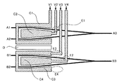
図1は、Xカット型基板に形成されたDC電極の一例を示す図である。図1では、2つのマッハツェンダー型導波路を並列配置した光変調器を示しているが、例えば、主マッハツェンダー型光導波路の2つの分岐導波路(A3,B3)に、副マッハツェンダー型光導波路(副マッハツェンダー型光導波路の分岐導波路は、A1とA2,B1とB2となる。)を入れ子型に組み込んだネスト型光導波路の一部が図示されている。 FIG. 1 is a diagram illustrating an example of a DC electrode formed on an X-cut substrate. FIG. 1 shows an optical modulator in which two Mach-Zehnder type waveguides are arranged in parallel. For example, sub-Mach-Zehnder type optical waveguides are provided in two branching waveguides (A3, B3) of the main Mach-Zehnder type optical waveguide. A part of a nested optical waveguide in which waveguides (the branching waveguides of the sub Mach-Zehnder optical waveguides are A1 and A2, B1 and B2) are nested is shown.
一方のマッハツェンダー型光導波路(A1〜A3)には、DC電極(C1,C2)が光導波路を挟むように形成され、各DC電極(C1,C2)にDCバイアス電圧(V1,V2)が印加される。また、他方のマッハツェンダー型光導波路(B1〜B3)には、DC電極(C3,C4)が光導波路を挟むように形成され、各DC電極(C3,C4)にDCバイアス電圧(V3,V4)が印加される。 On one of the Mach-Zehnder type optical waveguides (A1 to A3), DC electrodes (C1, C2) are formed so as to sandwich the optical waveguide, and a DC bias voltage (V1, V2) is applied to each DC electrode (C1, C2). Applied. The other Mach-Zehnder type optical waveguides (B1 to B3) are formed with DC electrodes (C3, C4) sandwiching the optical waveguide, and DC bias voltages (V3, V4) are applied to the DC electrodes (C3, C4). ) Is applied.
図1のDC電極では、例えば、点線E1と点線E2で示した箇所では、配線が光導波路(A1,B1)を横切ることとなる。このため、光導波路(A1)を伝搬する光波の一部が吸収され、分岐導波路A1と分岐導波路A2とでは、光の強度が異なり、両者を合成した場合の消光比が劣化する原因となっている。光導波路(B1〜B3)についても同様である。特に、ネスト型光導波路などのように、多数のマッハツェンダー型光導波路を組み込んだ光変調器においては、高速変調や多値変調など高度な変調技術が使用され、僅かな消光比の劣化も光変調器の特性に大きな影響を与える原因となる。 In the DC electrode of FIG. 1, for example, at locations indicated by dotted lines E <b> 1 and E <b> 2, the wiring crosses the optical waveguide (A <b> 1, B <b> 1). For this reason, a part of the light wave propagating through the optical waveguide (A1) is absorbed, the light intensity is different between the branched waveguide A1 and the branched waveguide A2, and the extinction ratio when the two are combined is deteriorated. It has become. The same applies to the optical waveguides (B1 to B3). In particular, optical modulators incorporating a large number of Mach-Zehnder optical waveguides, such as nested optical waveguides, use advanced modulation techniques such as high-speed modulation and multilevel modulation. It will cause a great influence on the characteristics of the modulator.
また、DC電極への給電が光変調器の一方の側面側から行われる場合など、DC電極の配線の取り回しにより、光導波路の対称軸(マッハツェンダー型光導波路の場合は、2つの分岐導波路の中間を通過する線)に対して配線の配置が非対称となり易い。図1では、点線E3の配線部分に対称となる部分(点線E4)には配線が存在しない。このような非対称性は、光導波路に電極(配線)が及ぼす内部応力が、各光導波路で異なる原因となり、各光導波路のモードフィールド径の変化によりさらなる消光比の劣化や、温度ドリフト現象(温度変化によりマッハツェンダー型光導波路の動作点がシフトする現象)を引き起こす。 In addition, when the power supply to the DC electrode is performed from one side of the optical modulator, the symmetrical axis of the optical waveguide (in the case of a Mach-Zehnder type optical waveguide, two branched waveguides) can be obtained by routing the wiring of the DC electrode. The wiring arrangement tends to be asymmetric with respect to the line passing through the middle of the line. In FIG. 1, there is no wiring in a portion (dotted line E4) that is symmetrical to the wiring portion of the dotted line E3. This asymmetry causes the internal stress exerted by the electrode (wiring) on the optical waveguide to be different in each optical waveguide, and the deterioration of the extinction ratio and the temperature drift phenomenon (temperature The change causes a phenomenon that the operating point of the Mach-Zehnder type optical waveguide shifts).
本発明が解決しようとする課題は、上述したような問題を解決し、消光比の劣化を抑制し、さらに温度ドリフト現象を抑制した光変調器を提供することである。 The problem to be solved by the present invention is to provide an optical modulator that solves the above-described problems, suppresses the deterioration of the extinction ratio, and further suppresses the temperature drift phenomenon.
上記課題を解決するため、本発明の光変調器は、次のような技術的特徴を備えている。
(1) 電気光学効果を有する基板と、該基板に形成された光導波路と、該光導波路を伝搬する光波を制御するための制御電極とを有する光変調器において、該光導波路は、少なくとも互いに並列に配置された2つのマッハツェンダー型光導波路を有し、該制御電極は、DCバイアスを印加するDC電極を有し、該DC電極にDCバイアスを給電する配線が接続され、各マッハツェンダー型光導波路に対して、該配線が該マッハツェンダー型光導波路の2つの分岐導波路の一方を横切っており、他方の分岐導波路の特定位置であって、該配線が前記一方の分岐導波路を横切った位置と相対的に対称となる特定位置に、第1のダミー電極を設け、一方のマッハツェンダー型光導波路の一部が、該配線及び該第1のダミー電極によって横切られており、他方のマッハツェンダー型光導波路の特定位置であって、該配線及び該第1のダミー電極が前記一方のマッハツェンダー型光導波路を横切った位置と相対的に対称となる特定位置に、第2のダミー電極を設け、さらに、該配線が、該マッハツェンダー型光導波路の延伸方向と平行に配置される平行配線部を有し、該延伸方向に平行かつ該マッハツェンダー型光導波路の対称軸となる中心軸に対し、該平行配線部と対称となる位置にほぼ同じ形状をした第3のダミー電極を形成したことを特徴とする。
In order to solve the above problems, the optical modulator of the present invention has the following technical features.
(1) In an optical modulator having a substrate having an electro-optic effect, an optical waveguide formed on the substrate, and a control electrode for controlling a light wave propagating through the optical waveguide, the optical waveguides are at least mutually It has two Mach-Zehnder type optical waveguides arranged in parallel, the control electrode has a DC electrode for applying a DC bias, and a wiring for supplying the DC bias is connected to the DC electrode. The wiring crosses one of the two branch waveguides of the Mach-Zehnder type optical waveguide with respect to the optical waveguide, and is located at a specific position of the other branch waveguide, and the wiring passes through the one branch waveguide. the particular position across a position between the relatively symmetrical, only set the first dummy electrode, part of one of the Mach-Zehnder type optical waveguide, you are crossed by the wiring and the first dummy electrode The specific position of the other Mach-Zehnder type optical waveguide is the specific position where the wiring and the first dummy electrode are relatively symmetrical with the position crossing the one Mach-Zehnder type optical waveguide. Two dummy electrodes are provided , and the wiring further includes a parallel wiring portion disposed in parallel with the extending direction of the Mach-Zehnder type optical waveguide, and is parallel to the extending direction and the axis of symmetry of the Mach-Zehnder type optical waveguide. A third dummy electrode having substantially the same shape is formed at a position symmetrical to the parallel wiring portion with respect to the central axis .
本発明における「ダミー電極」とは、光導波路にDCバイアスを印加する「DC電極」の役割は無く、該DC電極にDCバイアスを給電する配線により、マッハツェンダー型光導波路を構成する2つの分岐導波路で伝搬する光の強度が異なる場合に、両者の光波の伝搬損失を同程度に設定するために設けられた電極(図2のE5、E6参照。「第1のダミー電極」という。)や、2つの並列したマッハツェンダー型光導波路において、一方のマッハツェンダー型光導波路に設けられた該配線や該ダミー電極により、2つのマッハツェンダー型光導波路で伝搬する光強度が異なる場合に、両方のマッハツェンダー型光導波路で光波の伝搬損失を同程度に設定するために、他方のマッハツェンダー型光導波路に設けられた電極(図3のE7参照。「第2のダミー電極」という。)を意味する。The “dummy electrode” in the present invention has no role of “DC electrode” for applying a DC bias to the optical waveguide, and two branches constituting the Mach-Zehnder type optical waveguide by wiring for supplying the DC bias to the DC electrode. When the intensity of light propagating in the waveguide is different, electrodes provided to set the propagation loss of the two light waves to the same level (see E5 and E6 in FIG. 2, referred to as “first dummy electrode”). Or in two parallel Mach-Zehnder type optical waveguides, when the light intensity propagating in the two Mach-Zehnder type optical waveguides differs depending on the wiring or dummy electrode provided in one Mach-Zehnder type optical waveguide. In order to set the propagation loss of the light wave at the same level in the Mach-Zehnder type optical waveguide, the electrode provided on the other Mach-Zehnder type optical waveguide (see E7 in FIG. 3). That the second dummy electrode ".) Means.
また、本発明の「ダミー電極」には、DC電極にDCバイアスを給電する配線が、マッハツェンダー型光導波路の延伸方向と平行に配置される平行配線部を有し、該平行配線部により、マッハツェンダー型光導波路を構成する2つの分岐導波路に加わる内部応力が異なる場合に、2つの分岐導波路に加わる内部応力が等しくなるように設けられた電極(図5のE10や図6のE12参照。「第3のダミー電極」という。)も含まれる。 Further, in the “dummy electrode” of the present invention, a wiring for supplying a DC bias to the DC electrode has a parallel wiring portion arranged in parallel with the extending direction of the Mach-Zehnder optical waveguide, When the internal stress applied to the two branch waveguides constituting the Mach-Zehnder type optical waveguide is different, electrodes provided so that the internal stress applied to the two branch waveguides are equal (E10 in FIG. 5 or E12 in FIG. 6). See also “third dummy electrode”).
(2) 上記(1)に記載の光変調器において、該光導波路を横切る該配線又は該ダミー電極は、該光導波路を横切る部分の幅は、該光導波路を横切る前後の部分の幅よりも狭くなっていることを特徴とする。 (2) In the optical modulator according to (1 ), the width of the wiring or the dummy electrode that traverses the optical waveguide is wider than the width of the portion that crosses the optical waveguide. It is narrowed.
(3) 上記(1)又は(2)に記載の光変調器において、該DC電極を構成するホット電極と接地電極との間隔よりも、該第3のダミー電極と該第3のダミー電極に隣接する該配線との間隔の方が広くなるよう構成されていることを特徴とする。 (3) In the optical modulator described in the above (1) or (2), the third dummy electrode and the third dummy electrode are arranged more than the distance between the hot electrode and the ground electrode constituting the DC electrode. A feature is that the interval between the adjacent wirings is wider .
(4) 上記(1)乃至(3)のいずれかに記載の光変調器において、該ダミー電極は、該DC電極に電気的に接続されていることを特徴とする。 (4) The optical modulator according to any one of (1) to (3) , wherein the dummy electrode is electrically connected to the DC electrode.
本発明は、電気光学効果を有する基板と、該基板に形成された光導波路と、該光導波路を伝搬する光波を制御するための制御電極とを有する光変調器において、該光導波路は、少なくとも一つ以上のマッハツェンダー型光導波路を有し、該制御電極は、DCバイアスを印加するDC電極を有し、該DC電極にDCバイアスを給電する配線が、該マッハツェンダー型光導波路の2つの分岐導波路の一方を横切っており、他方の分岐導波路の特定位置であって、該配線が前記一方の分岐導波路を横切った位置と相対的に対称となる特定位置に、第1のダミー電極を設けるため、各分岐導波路による光波の伝搬損失を同程度に設定でき、光変調器の消光比の劣化を抑制することが可能となる。 The present invention provides an optical modulator having a substrate having an electro-optic effect, an optical waveguide formed on the substrate, and a control electrode for controlling a light wave propagating through the optical waveguide, wherein the optical waveguide includes at least One or more Mach-Zehnder type optical waveguides are provided, the control electrode has a DC electrode for applying a DC bias, and a wiring for supplying the DC bias to the DC electrodes has two wirings of the Mach-Zehnder type optical waveguide. The first dummy is crossed over one of the branching waveguides, at a specific position of the other branching waveguide, and the wiring is relatively symmetric with respect to the position crossing the one branching waveguide. Since the electrodes are provided, the propagation loss of the light wave by each branching waveguide can be set to the same level, and deterioration of the extinction ratio of the optical modulator can be suppressed.
しかも、配線が、マッハツェンダー型光導波路の延伸方向と平行に配置される平行配線部を有し、該延伸方向に平行かつ該マッハツェンダー型光導波路の対称軸となる中心軸に対し、該平行配線部と対称となる位置にほぼ同じ形状をした他のダミー電極(第3のダミー電極)を形成するため、DC電極により分岐導波路に加わる内部応力が等しくなるため、温度ドリフト現象の発生を抑制することも可能となる。 Moreover, the wiring has a parallel wiring portion arranged in parallel to the extending direction of the Mach-Zehnder type optical waveguide, and is parallel to the central axis that is parallel to the extending direction and that is the symmetry axis of the Mach-Zehnder type optical waveguide. In order to form another dummy electrode (third dummy electrode) having substantially the same shape at a position symmetrical to the wiring portion, the internal stress applied to the branching waveguide by the DC electrode becomes equal, so that the temperature drift phenomenon is generated. It can also be suppressed.
以下、本発明の光変調器について、好適例を用いて詳細に説明する。
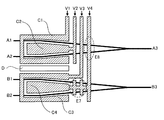
本発明の光変調器は、図2に示すように、電気光学効果を有する基板と、該基板に形成された光導波路と、該光導波路を伝搬する光波を制御するための制御電極とを有する光変調器において、該光導波路は、少なくとも一つ以上のマッハツェンダー型光導波路(A1〜A3,B1〜B3)を有し、該制御電極は、DCバイアスを印加するDC電極(C1〜C4)を有し、該DC電極にDCバイアスを給電する配線が、該マッハツェンダー型光導波路の2つの分岐導波路の一方を横切っており、他方の分岐導波路の特定位置であって、該配線が前記一方の分岐導波路を横切った位置と相対的に対称となる特定位置に、第1のダミー電極(点線E5,E6)を設けたことを特徴とする。
Hereinafter, the optical modulator of the present invention will be described in detail using preferred examples.
As shown in FIG. 2, the optical modulator of the present invention includes a substrate having an electro-optic effect, an optical waveguide formed on the substrate, and a control electrode for controlling a light wave propagating through the optical waveguide. In the optical modulator, the optical waveguide has at least one Mach-Zehnder optical waveguide (A1 to A3, B1 to B3), and the control electrode is a DC electrode (C1 to C4) for applying a DC bias. And a wiring for supplying a DC bias to the DC electrode crosses one of the two branch waveguides of the Mach-Zehnder optical waveguide, and is at a specific position of the other branch waveguide, A first dummy electrode (dotted lines E5 and E6) is provided at a specific position that is relatively symmetrical with the position crossing the one branching waveguide.
本発明の光変調器に用いる基板は、LiNbO3,LiTaO5又はPLZT(ジルコン酸チタン酸鉛ランタン)のいずれかの単結晶やInPなどの半導体、ポリマーなど、電気光学効果を有する基板が好適に利用可能である。特に、光変調器で多用されているLiNbO3,LiTaO5が好ましい。本発明の光変調器は、Xカット型基板を用いた光変調器により好適に適用されるが、Zカット型基板においても、制御電極により伝搬損失を伴う場合や、温度ドリフト現象が発生する場合には、適用することが好ましい。 The substrate used in the optical modulator of the present invention is preferably a substrate having an electrooptic effect, such as a single crystal of LiNbO 3 , LiTaO 5 or PLZT (lead lanthanum zirconate titanate), a semiconductor such as InP, or a polymer. Is available. In particular, LiNbO 3 and LiTaO 5 frequently used in optical modulators are preferable. The optical modulator of the present invention is preferably applied to an optical modulator using an X-cut type substrate. However, even in a Z-cut type substrate, a propagation loss is caused by a control electrode or a temperature drift phenomenon occurs. Is preferably applied.
基板には光導波路が形成されている。基板に形成する光導波路は、例えば、LiNbO3基板(LN基板)上にチタン(Ti)などを熱拡散することにより形成される。また、基板に光導波路に沿った凹凸を形成したリッジ型光導波路も利用可能である。光導波路のパターン形状としては、少なくとも一つのマッハツェンダー型導波路を備えており、例えば、複数のマッハツェンダー型導波路を組み合わせたネスト型導波路など、光変調器の用途に応じて種々の形状を採用することが可能である。 An optical waveguide is formed on the substrate. The optical waveguide formed on the substrate is formed, for example, by thermally diffusing titanium (Ti) or the like on a LiNbO 3 substrate (LN substrate). A ridge-type optical waveguide in which irregularities along the optical waveguide are formed on the substrate can also be used. The pattern shape of the optical waveguide includes at least one Mach-Zehnder type waveguide. For example, various shapes depending on the use of the optical modulator, such as a nested waveguide combining a plurality of Mach-Zehnder type waveguides. Can be adopted.
制御電極は、基板表面に、Ti・Auの電極パターンを形成し、金メッキ方法などにより形成することが可能である。本発明のダミー電極は、RF変調信号を印加する変調電極には適用することが難しく、専らDC電極に対して適用することが好ましい。 The control electrode can be formed by forming a Ti / Au electrode pattern on the substrate surface and using a gold plating method or the like. The dummy electrode of the present invention is difficult to apply to a modulation electrode that applies an RF modulation signal, and is preferably applied exclusively to a DC electrode.
DC電極は、図2に示すように、ホット電極(C2,C4)と接地電極(C1,C3)で構成される。隣接するマッハツェンダー型光導波路の間では、図2の符号Dに示すように、接地電極を別途配置している。これは、マッハツェンダー型光導波路に設けられたDC電極で発生した電界が、他の光導波路のDC電極に影響を及ぼすことを抑制するためである。 As shown in FIG. 2, the DC electrode includes hot electrodes (C2, C4) and ground electrodes (C1, C3). Between the adjacent Mach-Zehnder type optical waveguides, a ground electrode is separately disposed as shown by reference D in FIG. This is to prevent the electric field generated at the DC electrode provided in the Mach-Zehnder type optical waveguide from affecting the DC electrodes of other optical waveguides.
図2では、ホット電極(C2,C4)の配線の一部にダミー電極(点線E5,E6)を設けることで、分岐導波路のA1とA2、又はB1とB2との間で、導波光の伝搬損失を同程度に設定することを可能としている。ダミー電極は、ホット電極(C2,C4)だけでなく、接地電極(C1,C3)に設けることも可能である。 In FIG. 2, by providing dummy electrodes (dotted lines E5 and E6) on a part of the wiring of the hot electrodes (C2 and C4), the guided light is transmitted between the branched waveguides A1 and A2 or B1 and B2. It is possible to set the propagation loss to the same level. The dummy electrodes can be provided not only on the hot electrodes (C2, C4) but also on the ground electrodes (C1, C3).
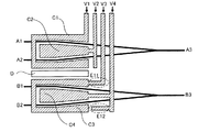
図3は、本発明の光変調器に関する第2の実施例を説明する図である。光導波路は、少なくとも互いに並列に配置された2つのマッハツェンダー型光導波路(A1〜A3とB1〜B3)を有し、一方のマッハツェンダー型光導波路(A1〜A3)の一部が、配線及びダミー電極によって横切られており、他方のマッハツェンダー型光導波路(B1〜B3)の特定位置であって、該配線及び該ダミー電極が前記一方のマッハツェンダー型光導波路を横切った位置と相対的に対称となる特定位置に、第2の他のダミー電極(点線E7)を設けたのである。 FIG. 3 is a diagram for explaining a second embodiment relating to the optical modulator of the present invention. The optical waveguide has at least two Mach-Zehnder type optical waveguides (A1 to A3 and B1 to B3) arranged in parallel to each other, and a part of one of the Mach-Zehnder type optical waveguides (A1 to A3) includes wiring and A specific position of the other Mach-Zehnder type optical waveguide (B1 to B3) crossed by the dummy electrode, relative to the position where the wiring and the dummy electrode cross the one Mach-Zehnder type optical waveguide The second other dummy electrode (dotted line E7) is provided at a specific position that is symmetrical.
図3のような構成を採用することで、マッハツェンダー型光導波路(A1〜A3)と他のマッハツェンダー型光導波路(B1〜B3)との間で、互いの伝搬損失を同程度に設定でき、この2つのマッハツェンダー型光導波路を合波した際の消光比を、高品質に維持することが可能になる。 By adopting the configuration as shown in FIG. 3, the mutual propagation loss can be set to the same level between the Mach-Zehnder type optical waveguides (A1 to A3) and the other Mach-Zehnder type optical waveguides (B1 to B3). The extinction ratio when the two Mach-Zehnder type optical waveguides are combined can be maintained with high quality.
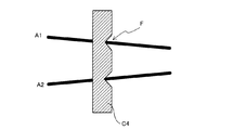
さらに、配線やダミー電極による導波光の伝搬損失を低減する方法としては、図3の点線E8の部分を拡大した図である図4に示すように、配線(又はダミー電極)が光導波路(A1,A2)を横切る部分の幅は、矢印Fのように、該光導波路を横切る前後の部分の幅よりも狭くすることが好ましい。 Further, as a method of reducing the propagation loss of guided light by the wiring and the dummy electrode, as shown in FIG. 4 which is an enlarged view of the dotted line E8 in FIG. 3, the wiring (or the dummy electrode) is an optical waveguide (A1). , A2), the width of the portion crossing the optical waveguide is preferably narrower than the width of the portion before and after the optical waveguide.
図5及び図6は、本発明の光変調器に関する第3及び第4の実施例を説明する図である。具体的には、配線が、マッハツェンダー型光導波路の延伸方向と平行に配置される平行配線部(E9,E11)を有し、該延伸方向に平行かつ該マッハツェンダー型光導波路の対称軸となる中心軸に対し、該平行配線部と対称となる位置にほぼ同じ形状をした第3のダミー電極(E10,E12)を形成したことを特徴とする。本構成により温度ドリフト現象を抑制し、更に消光比の劣化を抑制することできる。 5 and 6 are diagrams for explaining the third and fourth embodiments relating to the optical modulator of the present invention. Specifically, the wiring has parallel wiring portions (E9, E11) arranged parallel to the extending direction of the Mach-Zehnder type optical waveguide, and is parallel to the extending direction and the symmetry axis of the Mach-Zehnder type optical waveguide. A third dummy electrode (E10, E12) having substantially the same shape is formed at a position symmetrical to the parallel wiring portion with respect to the central axis. With this configuration, it is possible to suppress the temperature drift phenomenon and further suppress the deterioration of the extinction ratio.
図5は、接地電極(C3)側にダミー電極を設けており、図6は、ホット電極(C4)側にダミー電極を構成している。ダミー電極は、通常、DC電極(C1〜C4)に電気的に接続されていることが好ましく。これにより、ダミー電極の電位も安定させることが可能になる。また、ダミー電極は、ホット電極と接地電極の何れに接続してもよいが、DC電極が形成する電界の対称性を維持するためには、ダミー電極を設ける原因となる、非対称な形状を形成している配線と同じ種類の電極に接続することが望ましい。 In FIG. 5, a dummy electrode is provided on the ground electrode (C3) side, and in FIG. 6, a dummy electrode is configured on the hot electrode (C4) side. In general, the dummy electrode is preferably electrically connected to the DC electrodes (C1 to C4). Thereby, the potential of the dummy electrode can be stabilized. The dummy electrode may be connected to either the hot electrode or the ground electrode, but in order to maintain the symmetry of the electric field formed by the DC electrode, an asymmetric shape that causes the dummy electrode is formed. It is desirable to connect to the same type of electrode as the wiring being connected.
以上説明したように、本発明によれば、消光比の劣化を抑制し、さらに温度ドリフト現象を抑制した光変調器を提供することができる。 As described above, according to the present invention, it is possible to provide an optical modulator that suppresses the deterioration of the extinction ratio and further suppresses the temperature drift phenomenon.
A1〜A3,B1〜B3 光導波路
C1〜C4 DC電極
V1〜V4 DCバイアス電圧
D 接地電極
F 凹部
A1-A3, B1-B3 Optical waveguide C1-C4 DC electrode V1-V4 DC bias voltage D Ground electrode F Recess
Claims (4)
該光導波路は、少なくとも互いに並列に配置された2つのマッハツェンダー型光導波路を有し、
該制御電極は、DCバイアスを印加するDC電極を有し、
該DC電極にDCバイアスを給電する配線が接続され、
各マッハツェンダー型光導波路に対して、該配線が該マッハツェンダー型光導波路の2つの分岐導波路の一方を横切っており、他方の分岐導波路の特定位置であって、該配線が前記一方の分岐導波路を横切った位置と相対的に対称となる特定位置に、第1のダミー電極を設け、
一方のマッハツェンダー型光導波路の一部が、該配線及び該第1のダミー電極によって横切られており、他方のマッハツェンダー型光導波路の特定位置であって、該配線及び該第1のダミー電極が前記一方のマッハツェンダー型光導波路を横切った位置と相対的に対称となる特定位置に、第2のダミー電極を設け、
さらに、該配線が、該マッハツェンダー型光導波路の延伸方向と平行に配置される平行配線部を有し、該延伸方向に平行かつ該マッハツェンダー型光導波路の対称軸となる中心軸に対し、該平行配線部と対称となる位置にほぼ同じ形状をした第3のダミー電極を形成したことを特徴とする光変調器。 In an optical modulator having a substrate having an electro-optic effect, an optical waveguide formed on the substrate, and a control electrode for controlling a light wave propagating through the optical waveguide,
The optical waveguide has at least two Mach-Zehnder optical waveguides arranged in parallel with each other,
The control electrode has a DC electrode for applying a DC bias;
A wiring for supplying a DC bias is connected to the DC electrode,
For each Mach-Zehnder type optical waveguide, the wiring crosses one of the two branching waveguides of the Mach-Zehnder type optical waveguide, and is at a specific position of the other branching waveguide, and the wiring the particular position where the across the branching waveguides positioned relatively symmetrical, set the first dummy electrode,
A part of one Mach-Zehnder type optical waveguide is traversed by the wiring and the first dummy electrode, and the wiring and the first dummy electrode are at a specific position of the other Mach-Zehnder type optical waveguide. Is provided with a second dummy electrode at a specific position that is relatively symmetrical with the position across the one Mach-Zehnder optical waveguide ,
Further, the wiring has a parallel wiring portion disposed in parallel with the extending direction of the Mach-Zehnder type optical waveguide, and is parallel to the extending direction and a central axis that is a symmetry axis of the Mach-Zehnder type optical waveguide. 3. An optical modulator characterized in that a third dummy electrode having substantially the same shape is formed at a position symmetrical to the parallel wiring portion .
Priority Applications (4)
| Application Number | Priority Date | Filing Date | Title |
|---|---|---|---|
| JP2015071835A JP6233342B2 (en) | 2015-03-31 | 2015-03-31 | Light modulator |
| CN201680002409.4A CN106796362B (en) | 2015-03-31 | 2016-03-10 | light modulator |
| US15/514,505 US10409136B2 (en) | 2015-03-31 | 2016-03-10 | Optical modulator |
| PCT/JP2016/057520 WO2016158283A1 (en) | 2015-03-31 | 2016-03-10 | Light modulator |
Applications Claiming Priority (1)
| Application Number | Priority Date | Filing Date | Title |
|---|---|---|---|
| JP2015071835A JP6233342B2 (en) | 2015-03-31 | 2015-03-31 | Light modulator |
Publications (2)
| Publication Number | Publication Date |
|---|---|
| JP2016191827A JP2016191827A (en) | 2016-11-10 |
| JP6233342B2 true JP6233342B2 (en) | 2017-11-22 |
Family
ID=57004925
Family Applications (1)
| Application Number | Title | Priority Date | Filing Date |
|---|---|---|---|
| JP2015071835A Active JP6233342B2 (en) | 2015-03-31 | 2015-03-31 | Light modulator |
Country Status (4)
| Country | Link |
|---|---|
| US (1) | US10409136B2 (en) |
| JP (1) | JP6233342B2 (en) |
| CN (1) | CN106796362B (en) |
| WO (1) | WO2016158283A1 (en) |
Families Citing this family (2)
| Publication number | Priority date | Publication date | Assignee | Title |
|---|---|---|---|---|
| CN109031708A (en) * | 2018-09-29 | 2018-12-18 | 深圳市芯思杰智慧传感技术有限公司 | A kind of optical waveguide phase-modulator chip with pre- phase-modulation function |
| CN116699921A (en) * | 2022-02-25 | 2023-09-05 | 华为技术有限公司 | Mach-Zehnder modulator, electro-optic modulation method and light emitting device |
Family Cites Families (11)
| Publication number | Priority date | Publication date | Assignee | Title |
|---|---|---|---|---|
| JP3195033B2 (en) * | 1992-03-10 | 2001-08-06 | 日本放送協会 | Optical waveguide and method for forming the same |
| DE69523104T2 (en) * | 1994-02-11 | 2002-06-06 | Koninklijke Philips Electronics N.V., Eindhoven | PHASE COUPLED OPTICAL DEVICE |
| JPH09211403A (en) * | 1996-02-01 | 1997-08-15 | Nippon Telegr & Teleph Corp <Ntt> | Light control element |
| JPH11271699A (en) * | 1998-03-26 | 1999-10-08 | Ngk Insulators Ltd | Optical waveguide device |
| JP3841793B2 (en) * | 2004-02-26 | 2006-11-01 | 独立行政法人情報通信研究機構 | Frequency conversion method and base station in wireless optical fusion communication system |
| JP2007025370A (en) * | 2005-07-19 | 2007-02-01 | Ricoh Co Ltd | Organic waveguide type optical modulator and optical communication system |
| JP4774037B2 (en) * | 2007-12-28 | 2011-09-14 | 日本電信電話株式会社 | Waveguide type optical circuit |
| JP2009181108A (en) * | 2008-02-01 | 2009-08-13 | Sumitomo Osaka Cement Co Ltd | Optical waveguide element |
| JP4388987B2 (en) * | 2008-03-31 | 2009-12-24 | 住友大阪セメント株式会社 | Mach-Zehnder waveguide type optical modulator |
| EP2453295B1 (en) * | 2009-07-10 | 2014-09-10 | Nippon Telegraph And Telephone Corporation | Optical modulator |
| JP5487774B2 (en) * | 2009-07-27 | 2014-05-07 | 富士通オプティカルコンポーネンツ株式会社 | Optical device and optical transmitter |
-
2015
- 2015-03-31 JP JP2015071835A patent/JP6233342B2/en active Active
-
2016
- 2016-03-10 CN CN201680002409.4A patent/CN106796362B/en active Active
- 2016-03-10 WO PCT/JP2016/057520 patent/WO2016158283A1/en not_active Ceased
- 2016-03-10 US US15/514,505 patent/US10409136B2/en active Active
Also Published As
| Publication number | Publication date |
|---|---|
| CN106796362B (en) | 2021-05-28 |
| JP2016191827A (en) | 2016-11-10 |
| WO2016158283A1 (en) | 2016-10-06 |
| US10409136B2 (en) | 2019-09-10 |
| US20180307116A1 (en) | 2018-10-25 |
| CN106796362A (en) | 2017-05-31 |
Similar Documents
| Publication | Publication Date | Title |
|---|---|---|
| JP5326860B2 (en) | Optical waveguide device | |
| JP5120341B2 (en) | Optical device | |
| US7447389B2 (en) | Optical modulator | |
| JP5092573B2 (en) | Optical waveguide device | |
| JP5067464B2 (en) | Light control element | |
| JP5007629B2 (en) | Optical waveguide device | |
| JP6107869B2 (en) | Light modulator | |
| JP2014071383A (en) | Optical modulator | |
| CN106662766A (en) | Optical waveguide element | |
| JP5077480B2 (en) | Optical waveguide device | |
| JPWO2008117449A1 (en) | Optical device | |
| JP4151798B2 (en) | Light modulator | |
| JP6233342B2 (en) | Light modulator | |
| JP5229378B2 (en) | Optical waveguide device | |
| JP6222250B2 (en) | Optical modulator and optical transmitter using the same | |
| JP4703158B2 (en) | Light control element | |
| JP2010134115A (en) | Light modulator | |
| JP2017032753A (en) | Optical modulator and optical transmitter using the same | |
| JP6084177B2 (en) | Optical waveguide device | |
| JP2008009314A (en) | Optical waveguide element, optical modulator, and optical communication device | |
| JP4544479B2 (en) | Optical waveguide modulator | |
| JP5428716B2 (en) | Directional coupler | |
| JP2014199354A (en) | Optical modulator |
Legal Events
| Date | Code | Title | Description |
|---|---|---|---|
| A131 | Notification of reasons for refusal |
Free format text: JAPANESE INTERMEDIATE CODE: A131 Effective date: 20170207 |
|
| A521 | Written amendment |
Free format text: JAPANESE INTERMEDIATE CODE: A523 Effective date: 20170410 |
|
| TRDD | Decision of grant or rejection written | ||
| A01 | Written decision to grant a patent or to grant a registration (utility model) |
Free format text: JAPANESE INTERMEDIATE CODE: A01 Effective date: 20170926 |
|
| A61 | First payment of annual fees (during grant procedure) |
Free format text: JAPANESE INTERMEDIATE CODE: A61 Effective date: 20171009 |
|
| R150 | Certificate of patent or registration of utility model |
Ref document number: 6233342 Country of ref document: JP Free format text: JAPANESE INTERMEDIATE CODE: R150 |