JP6233342B2 - 光変調器 - Google Patents
光変調器 Download PDFInfo
- Publication number
- JP6233342B2 JP6233342B2 JP2015071835A JP2015071835A JP6233342B2 JP 6233342 B2 JP6233342 B2 JP 6233342B2 JP 2015071835 A JP2015071835 A JP 2015071835A JP 2015071835 A JP2015071835 A JP 2015071835A JP 6233342 B2 JP6233342 B2 JP 6233342B2
- Authority
- JP
- Japan
- Prior art keywords
- electrode
- optical waveguide
- mach
- wiring
- zehnder type
- Prior art date
- Legal status (The legal status is an assumption and is not a legal conclusion. Google has not performed a legal analysis and makes no representation as to the accuracy of the status listed.)
- Active
Links
- 230000003287 optical effect Effects 0.000 claims description 141
- 239000000758 substrate Substances 0.000 claims description 29
- 230000001902 propagating effect Effects 0.000 claims description 11
- 230000000694 effects Effects 0.000 claims description 7
- 230000008033 biological extinction Effects 0.000 description 7
- 230000006866 deterioration Effects 0.000 description 5
- 230000005684 electric field Effects 0.000 description 4
- 229910013641 LiNbO 3 Inorganic materials 0.000 description 3
- 238000010586 diagram Methods 0.000 description 3
- GQYHUHYESMUTHG-UHFFFAOYSA-N lithium niobate Chemical compound [Li+].[O-][Nb](=O)=O GQYHUHYESMUTHG-UHFFFAOYSA-N 0.000 description 3
- 238000000034 method Methods 0.000 description 3
- 239000010936 titanium Substances 0.000 description 3
- RTAQQCXQSZGOHL-UHFFFAOYSA-N Titanium Chemical compound [Ti] RTAQQCXQSZGOHL-UHFFFAOYSA-N 0.000 description 2
- 239000010931 gold Substances 0.000 description 2
- 239000013078 crystal Substances 0.000 description 1
- PCHJSUWPFVWCPO-UHFFFAOYSA-N gold Chemical compound [Au] PCHJSUWPFVWCPO-UHFFFAOYSA-N 0.000 description 1
- 229910052737 gold Inorganic materials 0.000 description 1
- 229910052746 lanthanum Inorganic materials 0.000 description 1
- FZLIPJUXYLNCLC-UHFFFAOYSA-N lanthanum atom Chemical compound [La] FZLIPJUXYLNCLC-UHFFFAOYSA-N 0.000 description 1
- 238000005259 measurement Methods 0.000 description 1
- 238000007747 plating Methods 0.000 description 1
- 229920000642 polymer Polymers 0.000 description 1
- 239000004065 semiconductor Substances 0.000 description 1
- 229910052719 titanium Inorganic materials 0.000 description 1
Images


Classifications
-
- G—PHYSICS
- G02—OPTICS
- G02F—OPTICAL DEVICES OR ARRANGEMENTS FOR THE CONTROL OF LIGHT BY MODIFICATION OF THE OPTICAL PROPERTIES OF THE MEDIA OF THE ELEMENTS INVOLVED THEREIN; NON-LINEAR OPTICS; FREQUENCY-CHANGING OF LIGHT; OPTICAL LOGIC ELEMENTS; OPTICAL ANALOGUE/DIGITAL CONVERTERS
- G02F1/00—Devices or arrangements for the control of the intensity, colour, phase, polarisation or direction of light arriving from an independent light source, e.g. switching, gating or modulating; Non-linear optics
- G02F1/01—Devices or arrangements for the control of the intensity, colour, phase, polarisation or direction of light arriving from an independent light source, e.g. switching, gating or modulating; Non-linear optics for the control of the intensity, phase, polarisation or colour
- G02F1/21—Devices or arrangements for the control of the intensity, colour, phase, polarisation or direction of light arriving from an independent light source, e.g. switching, gating or modulating; Non-linear optics for the control of the intensity, phase, polarisation or colour by interference
- G02F1/225—Devices or arrangements for the control of the intensity, colour, phase, polarisation or direction of light arriving from an independent light source, e.g. switching, gating or modulating; Non-linear optics for the control of the intensity, phase, polarisation or colour by interference in an optical waveguide structure
-
- G—PHYSICS
- G02—OPTICS
- G02F—OPTICAL DEVICES OR ARRANGEMENTS FOR THE CONTROL OF LIGHT BY MODIFICATION OF THE OPTICAL PROPERTIES OF THE MEDIA OF THE ELEMENTS INVOLVED THEREIN; NON-LINEAR OPTICS; FREQUENCY-CHANGING OF LIGHT; OPTICAL LOGIC ELEMENTS; OPTICAL ANALOGUE/DIGITAL CONVERTERS
- G02F1/00—Devices or arrangements for the control of the intensity, colour, phase, polarisation or direction of light arriving from an independent light source, e.g. switching, gating or modulating; Non-linear optics
- G02F1/01—Devices or arrangements for the control of the intensity, colour, phase, polarisation or direction of light arriving from an independent light source, e.g. switching, gating or modulating; Non-linear optics for the control of the intensity, phase, polarisation or colour
- G02F1/0121—Operation of devices; Circuit arrangements, not otherwise provided for in this subclass
- G02F1/0123—Circuits for the control or stabilisation of the bias voltage, e.g. automatic bias control [ABC] feedback loops
-
- G—PHYSICS
- G02—OPTICS
- G02F—OPTICAL DEVICES OR ARRANGEMENTS FOR THE CONTROL OF LIGHT BY MODIFICATION OF THE OPTICAL PROPERTIES OF THE MEDIA OF THE ELEMENTS INVOLVED THEREIN; NON-LINEAR OPTICS; FREQUENCY-CHANGING OF LIGHT; OPTICAL LOGIC ELEMENTS; OPTICAL ANALOGUE/DIGITAL CONVERTERS
- G02F1/00—Devices or arrangements for the control of the intensity, colour, phase, polarisation or direction of light arriving from an independent light source, e.g. switching, gating or modulating; Non-linear optics
- G02F1/01—Devices or arrangements for the control of the intensity, colour, phase, polarisation or direction of light arriving from an independent light source, e.g. switching, gating or modulating; Non-linear optics for the control of the intensity, phase, polarisation or colour
- G02F1/21—Devices or arrangements for the control of the intensity, colour, phase, polarisation or direction of light arriving from an independent light source, e.g. switching, gating or modulating; Non-linear optics for the control of the intensity, phase, polarisation or colour by interference
- G02F1/212—Mach-Zehnder type
-
- G—PHYSICS
- G02—OPTICS
- G02F—OPTICAL DEVICES OR ARRANGEMENTS FOR THE CONTROL OF LIGHT BY MODIFICATION OF THE OPTICAL PROPERTIES OF THE MEDIA OF THE ELEMENTS INVOLVED THEREIN; NON-LINEAR OPTICS; FREQUENCY-CHANGING OF LIGHT; OPTICAL LOGIC ELEMENTS; OPTICAL ANALOGUE/DIGITAL CONVERTERS
- G02F2201/00—Constructional arrangements not provided for in groups G02F1/00 - G02F7/00
- G02F2201/12—Constructional arrangements not provided for in groups G02F1/00 - G02F7/00 electrode
-
- G—PHYSICS
- G02—OPTICS
- G02F—OPTICAL DEVICES OR ARRANGEMENTS FOR THE CONTROL OF LIGHT BY MODIFICATION OF THE OPTICAL PROPERTIES OF THE MEDIA OF THE ELEMENTS INVOLVED THEREIN; NON-LINEAR OPTICS; FREQUENCY-CHANGING OF LIGHT; OPTICAL LOGIC ELEMENTS; OPTICAL ANALOGUE/DIGITAL CONVERTERS
- G02F2202/00—Materials and properties
- G02F2202/20—LiNbO3, LiTaO3
-
- G—PHYSICS
- G02—OPTICS
- G02F—OPTICAL DEVICES OR ARRANGEMENTS FOR THE CONTROL OF LIGHT BY MODIFICATION OF THE OPTICAL PROPERTIES OF THE MEDIA OF THE ELEMENTS INVOLVED THEREIN; NON-LINEAR OPTICS; FREQUENCY-CHANGING OF LIGHT; OPTICAL LOGIC ELEMENTS; OPTICAL ANALOGUE/DIGITAL CONVERTERS
- G02F2203/00—Function characteristic
- G02F2203/21—Thermal instability, i.e. DC drift, of an optical modulator; Arrangements or methods for the reduction thereof
Landscapes
- Physics & Mathematics (AREA)
- Nonlinear Science (AREA)
- General Physics & Mathematics (AREA)
- Optics & Photonics (AREA)
- Optical Modulation, Optical Deflection, Nonlinear Optics, Optical Demodulation, Optical Logic Elements (AREA)
Description
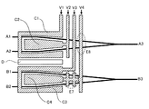
(1) 電気光学効果を有する基板と、該基板に形成された光導波路と、該光導波路を伝搬する光波を制御するための制御電極とを有する光変調器において、該光導波路は、少なくとも互いに並列に配置された2つのマッハツェンダー型光導波路を有し、該制御電極は、DCバイアスを印加するDC電極を有し、該DC電極にDCバイアスを給電する配線が接続され、各マッハツェンダー型光導波路に対して、該配線が該マッハツェンダー型光導波路の2つの分岐導波路の一方を横切っており、他方の分岐導波路の特定位置であって、該配線が前記一方の分岐導波路を横切った位置と相対的に対称となる特定位置に、第1のダミー電極を設け、一方のマッハツェンダー型光導波路の一部が、該配線及び該第1のダミー電極によって横切られており、他方のマッハツェンダー型光導波路の特定位置であって、該配線及び該第1のダミー電極が前記一方のマッハツェンダー型光導波路を横切った位置と相対的に対称となる特定位置に、第2のダミー電極を設け、さらに、該配線が、該マッハツェンダー型光導波路の延伸方向と平行に配置される平行配線部を有し、該延伸方向に平行かつ該マッハツェンダー型光導波路の対称軸となる中心軸に対し、該平行配線部と対称となる位置にほぼ同じ形状をした第3のダミー電極を形成したことを特徴とする。
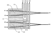
また、本発明の「ダミー電極」には、DC電極にDCバイアスを給電する配線が、マッハツェンダー型光導波路の延伸方向と平行に配置される平行配線部を有し、該平行配線部により、マッハツェンダー型光導波路を構成する2つの分岐導波路に加わる内部応力が異なる場合に、2つの分岐導波路に加わる内部応力が等しくなるように設けられた電極(図5のE10や図6のE12参照。「第3のダミー電極」という。)も含まれる。
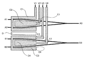
本発明の光変調器は、図2に示すように、電気光学効果を有する基板と、該基板に形成された光導波路と、該光導波路を伝搬する光波を制御するための制御電極とを有する光変調器において、該光導波路は、少なくとも一つ以上のマッハツェンダー型光導波路(A1〜A3,B1〜B3)を有し、該制御電極は、DCバイアスを印加するDC電極(C1〜C4)を有し、該DC電極にDCバイアスを給電する配線が、該マッハツェンダー型光導波路の2つの分岐導波路の一方を横切っており、他方の分岐導波路の特定位置であって、該配線が前記一方の分岐導波路を横切った位置と相対的に対称となる特定位置に、第1のダミー電極(点線E5,E6)を設けたことを特徴とする。
C1〜C4 DC電極
V1〜V4 DCバイアス電圧
D 接地電極
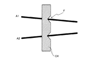
F 凹部
Claims (4)
- 電気光学効果を有する基板と、該基板に形成された光導波路と、該光導波路を伝搬する光波を制御するための制御電極とを有する光変調器において、
該光導波路は、少なくとも互いに並列に配置された2つのマッハツェンダー型光導波路を有し、
該制御電極は、DCバイアスを印加するDC電極を有し、
該DC電極にDCバイアスを給電する配線が接続され、
各マッハツェンダー型光導波路に対して、該配線が該マッハツェンダー型光導波路の2つの分岐導波路の一方を横切っており、他方の分岐導波路の特定位置であって、該配線が前記一方の分岐導波路を横切った位置と相対的に対称となる特定位置に、第1のダミー電極を設け、
一方のマッハツェンダー型光導波路の一部が、該配線及び該第1のダミー電極によって横切られており、他方のマッハツェンダー型光導波路の特定位置であって、該配線及び該第1のダミー電極が前記一方のマッハツェンダー型光導波路を横切った位置と相対的に対称となる特定位置に、第2のダミー電極を設け、
さらに、該配線が、該マッハツェンダー型光導波路の延伸方向と平行に配置される平行配線部を有し、該延伸方向に平行かつ該マッハツェンダー型光導波路の対称軸となる中心軸に対し、該平行配線部と対称となる位置にほぼ同じ形状をした第3のダミー電極を形成したことを特徴とする光変調器。 - 請求項1に記載の光変調器において、該光導波路を横切る該配線又は該ダミー電極は、該光導波路を横切る部分の幅は、該光導波路を横切る前後の部分の幅よりも狭くなっていることを特徴とする光変調器。
- 請求項1又は2に記載の光変調器において、該DC電極を構成するホット電極と接地電極との間隔よりも、該第3のダミー電極と該第3のダミー電極に隣接する該配線との間隔の方が広くなるよう構成されていることを特徴とする光変調器。
- 請求項1乃至3のいずれかに記載の光変調器において、該ダミー電極は、該DC電極に電気的に接続されていることを特徴とする光変調器。
Priority Applications (4)
| Application Number | Priority Date | Filing Date | Title |
|---|---|---|---|
| JP2015071835A JP6233342B2 (ja) | 2015-03-31 | 2015-03-31 | 光変調器 |
| US15/514,505 US10409136B2 (en) | 2015-03-31 | 2016-03-10 | Optical modulator |
| PCT/JP2016/057520 WO2016158283A1 (ja) | 2015-03-31 | 2016-03-10 | 光変調器 |
| CN201680002409.4A CN106796362B (zh) | 2015-03-31 | 2016-03-10 | 光调制器 |
Applications Claiming Priority (1)
| Application Number | Priority Date | Filing Date | Title |
|---|---|---|---|
| JP2015071835A JP6233342B2 (ja) | 2015-03-31 | 2015-03-31 | 光変調器 |
Publications (2)
| Publication Number | Publication Date |
|---|---|
| JP2016191827A JP2016191827A (ja) | 2016-11-10 |
| JP6233342B2 true JP6233342B2 (ja) | 2017-11-22 |
Family
ID=57004925
Family Applications (1)
| Application Number | Title | Priority Date | Filing Date |
|---|---|---|---|
| JP2015071835A Active JP6233342B2 (ja) | 2015-03-31 | 2015-03-31 | 光変調器 |
Country Status (4)
| Country | Link |
|---|---|
| US (1) | US10409136B2 (ja) |
| JP (1) | JP6233342B2 (ja) |
| CN (1) | CN106796362B (ja) |
| WO (1) | WO2016158283A1 (ja) |
Families Citing this family (2)
| Publication number | Priority date | Publication date | Assignee | Title |
|---|---|---|---|---|
| CN109031708A (zh) * | 2018-09-29 | 2018-12-18 | 深圳市芯思杰智慧传感技术有限公司 | 一种具有预相位调制功能的光波导相位调制器芯片 |
| CN116699921A (zh) * | 2022-02-25 | 2023-09-05 | 华为技术有限公司 | 一种马赫曾德调制器、电光调制方法和光发射装置 |
Family Cites Families (11)
| Publication number | Priority date | Publication date | Assignee | Title |
|---|---|---|---|---|
| JP3195033B2 (ja) * | 1992-03-10 | 2001-08-06 | 日本放送協会 | 光導波路およびその形成方法 |
| JP3425150B2 (ja) * | 1994-02-11 | 2003-07-07 | コーニンクレッカ、フィリップス、エレクトロニクス、エヌ.ヴィ. | 位相調整アレイを有する光学装置 |
| JPH09211403A (ja) * | 1996-02-01 | 1997-08-15 | Nippon Telegr & Teleph Corp <Ntt> | 光制御素子 |
| JPH11271699A (ja) * | 1998-03-26 | 1999-10-08 | Ngk Insulators Ltd | 光導波路素子 |
| JP3841793B2 (ja) | 2004-02-26 | 2006-11-01 | 独立行政法人情報通信研究機構 | 無線光融合通信システムにおける周波数変換方法及び基地局 |
| JP2007025370A (ja) * | 2005-07-19 | 2007-02-01 | Ricoh Co Ltd | 有機導波路型光変調器・光通信システム |
| JP4774037B2 (ja) * | 2007-12-28 | 2011-09-14 | 日本電信電話株式会社 | 導波路型光回路 |
| JP2009181108A (ja) * | 2008-02-01 | 2009-08-13 | Sumitomo Osaka Cement Co Ltd | 光導波路素子 |
| JP4388987B2 (ja) * | 2008-03-31 | 2009-12-24 | 住友大阪セメント株式会社 | マッハツェンダー導波路型光変調器 |
| WO2011004615A1 (ja) * | 2009-07-10 | 2011-01-13 | 日本電信電話株式会社 | 光変調器 |
| JP5487774B2 (ja) | 2009-07-27 | 2014-05-07 | 富士通オプティカルコンポーネンツ株式会社 | 光デバイスおよび光送信機 |
-
2015
- 2015-03-31 JP JP2015071835A patent/JP6233342B2/ja active Active
-
2016
- 2016-03-10 WO PCT/JP2016/057520 patent/WO2016158283A1/ja not_active Ceased
- 2016-03-10 CN CN201680002409.4A patent/CN106796362B/zh active Active
- 2016-03-10 US US15/514,505 patent/US10409136B2/en active Active
Also Published As
| Publication number | Publication date |
|---|---|
| WO2016158283A1 (ja) | 2016-10-06 |
| JP2016191827A (ja) | 2016-11-10 |
| CN106796362B (zh) | 2021-05-28 |
| US20180307116A1 (en) | 2018-10-25 |
| CN106796362A (zh) | 2017-05-31 |
| US10409136B2 (en) | 2019-09-10 |
Similar Documents
| Publication | Publication Date | Title |
|---|---|---|
| JP5326860B2 (ja) | 光導波路デバイス | |
| JP5120341B2 (ja) | 光デバイス | |
| US7447389B2 (en) | Optical modulator | |
| JP5092573B2 (ja) | 光導波路デバイス | |
| JP5067464B2 (ja) | 光制御素子 | |
| JP5007629B2 (ja) | 光導波路素子 | |
| JP6107869B2 (ja) | 光変調器 | |
| JP2014071383A (ja) | 光変調器 | |
| CN106662766A (zh) | 光波导元件 | |
| JP5077480B2 (ja) | 光導波路素子 | |
| JPWO2008117449A1 (ja) | 光デバイス | |
| JP4151798B2 (ja) | 光変調器 | |
| JP6233342B2 (ja) | 光変調器 | |
| JP5229378B2 (ja) | 光導波路素子 | |
| JP6222250B2 (ja) | 光変調器及びそれを用いた光送信装置 | |
| JP4703158B2 (ja) | 光制御素子 | |
| JP2017032753A (ja) | 光変調器及びそれを用いた光送信装置 | |
| JP6084177B2 (ja) | 光導波路デバイス | |
| JP2008009314A (ja) | 光導波路素子、光変調器および光通信装置 | |
| JP4544479B2 (ja) | 光導波路型変調器 | |
| JP5428716B2 (ja) | 方向性結合器 | |
| JP2014199354A (ja) | 光変調器 |
Legal Events
| Date | Code | Title | Description |
|---|---|---|---|
| A131 | Notification of reasons for refusal |
Free format text: JAPANESE INTERMEDIATE CODE: A131 Effective date: 20170207 |
|
| A521 | Written amendment |
Free format text: JAPANESE INTERMEDIATE CODE: A523 Effective date: 20170410 |
|
| TRDD | Decision of grant or rejection written | ||
| A01 | Written decision to grant a patent or to grant a registration (utility model) |
Free format text: JAPANESE INTERMEDIATE CODE: A01 Effective date: 20170926 |
|
| A61 | First payment of annual fees (during grant procedure) |
Free format text: JAPANESE INTERMEDIATE CODE: A61 Effective date: 20171009 |
|
| R150 | Certificate of patent or registration of utility model |
Ref document number: 6233342 Country of ref document: JP Free format text: JAPANESE INTERMEDIATE CODE: R150 |