JP6233936B2 - ウェハをダイに分割する方法 - Google Patents
ウェハをダイに分割する方法 Download PDFInfo
- Publication number
- JP6233936B2 JP6233936B2 JP2015230840A JP2015230840A JP6233936B2 JP 6233936 B2 JP6233936 B2 JP 6233936B2 JP 2015230840 A JP2015230840 A JP 2015230840A JP 2015230840 A JP2015230840 A JP 2015230840A JP 6233936 B2 JP6233936 B2 JP 6233936B2
- Authority
- JP
- Japan
- Prior art keywords
- wafer
- carrier
- adhesive tape
- adhesive
- connecting means
- Prior art date
- Legal status (The legal status is an assumption and is not a legal conclusion. Google has not performed a legal analysis and makes no representation as to the accuracy of the status listed.)
- Active
Links
Images






Classifications
-
- H—ELECTRICITY
- H10—SEMICONDUCTOR DEVICES; ELECTRIC SOLID-STATE DEVICES NOT OTHERWISE PROVIDED FOR
- H10P—GENERIC PROCESSES OR APPARATUS FOR THE MANUFACTURE OR TREATMENT OF DEVICES COVERED BY CLASS H10
- H10P72/00—Handling or holding of wafers, substrates or devices during manufacture or treatment thereof
- H10P72/04—Apparatus for manufacture or treatment
- H10P72/0442—Apparatus for placing on an insulating substrate, e.g. tape
-
- H—ELECTRICITY
- H10—SEMICONDUCTOR DEVICES; ELECTRIC SOLID-STATE DEVICES NOT OTHERWISE PROVIDED FOR
- H10P—GENERIC PROCESSES OR APPARATUS FOR THE MANUFACTURE OR TREATMENT OF DEVICES COVERED BY CLASS H10
- H10P54/00—Cutting or separating of wafers, substrates or parts of devices
-
- H—ELECTRICITY
- H10—SEMICONDUCTOR DEVICES; ELECTRIC SOLID-STATE DEVICES NOT OTHERWISE PROVIDED FOR
- H10P—GENERIC PROCESSES OR APPARATUS FOR THE MANUFACTURE OR TREATMENT OF DEVICES COVERED BY CLASS H10
- H10P72/00—Handling or holding of wafers, substrates or devices during manufacture or treatment thereof
- H10P72/70—Handling or holding of wafers, substrates or devices during manufacture or treatment thereof for supporting or gripping
- H10P72/74—Handling or holding of wafers, substrates or devices during manufacture or treatment thereof for supporting or gripping using temporarily an auxiliary support
-
- H—ELECTRICITY
- H10—SEMICONDUCTOR DEVICES; ELECTRIC SOLID-STATE DEVICES NOT OTHERWISE PROVIDED FOR
- H10P—GENERIC PROCESSES OR APPARATUS FOR THE MANUFACTURE OR TREATMENT OF DEVICES COVERED BY CLASS H10
- H10P72/00—Handling or holding of wafers, substrates or devices during manufacture or treatment thereof
- H10P72/70—Handling or holding of wafers, substrates or devices during manufacture or treatment thereof for supporting or gripping
- H10P72/74—Handling or holding of wafers, substrates or devices during manufacture or treatment thereof for supporting or gripping using temporarily an auxiliary support
- H10P72/7402—Wafer tapes, e.g. grinding or dicing support tapes
-
- H—ELECTRICITY
- H10—SEMICONDUCTOR DEVICES; ELECTRIC SOLID-STATE DEVICES NOT OTHERWISE PROVIDED FOR
- H10P—GENERIC PROCESSES OR APPARATUS FOR THE MANUFACTURE OR TREATMENT OF DEVICES COVERED BY CLASS H10
- H10P90/00—Preparation of wafers not covered by a single main group of this subclass, e.g. wafer reinforcement
- H10P90/12—Preparing bulk and homogeneous wafers
- H10P90/123—Preparing bulk and homogeneous wafers by grinding or lapping
-
- H—ELECTRICITY
- H10—SEMICONDUCTOR DEVICES; ELECTRIC SOLID-STATE DEVICES NOT OTHERWISE PROVIDED FOR
- H10P—GENERIC PROCESSES OR APPARATUS FOR THE MANUFACTURE OR TREATMENT OF DEVICES COVERED BY CLASS H10
- H10P72/00—Handling or holding of wafers, substrates or devices during manufacture or treatment thereof
- H10P72/70—Handling or holding of wafers, substrates or devices during manufacture or treatment thereof for supporting or gripping
- H10P72/74—Handling or holding of wafers, substrates or devices during manufacture or treatment thereof for supporting or gripping using temporarily an auxiliary support
- H10P72/7412—Handling or holding of wafers, substrates or devices during manufacture or treatment thereof for supporting or gripping using temporarily an auxiliary support the auxiliary support including means facilitating the separation of a device or wafer from the auxiliary support
-
- H—ELECTRICITY
- H10—SEMICONDUCTOR DEVICES; ELECTRIC SOLID-STATE DEVICES NOT OTHERWISE PROVIDED FOR
- H10P—GENERIC PROCESSES OR APPARATUS FOR THE MANUFACTURE OR TREATMENT OF DEVICES COVERED BY CLASS H10
- H10P72/00—Handling or holding of wafers, substrates or devices during manufacture or treatment thereof
- H10P72/70—Handling or holding of wafers, substrates or devices during manufacture or treatment thereof for supporting or gripping
- H10P72/74—Handling or holding of wafers, substrates or devices during manufacture or treatment thereof for supporting or gripping using temporarily an auxiliary support
- H10P72/7416—Handling or holding of wafers, substrates or devices during manufacture or treatment thereof for supporting or gripping using temporarily an auxiliary support used during dicing or grinding
-
- H—ELECTRICITY
- H10—SEMICONDUCTOR DEVICES; ELECTRIC SOLID-STATE DEVICES NOT OTHERWISE PROVIDED FOR
- H10P—GENERIC PROCESSES OR APPARATUS FOR THE MANUFACTURE OR TREATMENT OF DEVICES COVERED BY CLASS H10
- H10P72/00—Handling or holding of wafers, substrates or devices during manufacture or treatment thereof
- H10P72/70—Handling or holding of wafers, substrates or devices during manufacture or treatment thereof for supporting or gripping
- H10P72/74—Handling or holding of wafers, substrates or devices during manufacture or treatment thereof for supporting or gripping using temporarily an auxiliary support
- H10P72/7422—Handling or holding of wafers, substrates or devices during manufacture or treatment thereof for supporting or gripping using temporarily an auxiliary support used to protect an active side of a device or wafer
-
- H—ELECTRICITY
- H10—SEMICONDUCTOR DEVICES; ELECTRIC SOLID-STATE DEVICES NOT OTHERWISE PROVIDED FOR
- H10P—GENERIC PROCESSES OR APPARATUS FOR THE MANUFACTURE OR TREATMENT OF DEVICES COVERED BY CLASS H10
- H10P72/00—Handling or holding of wafers, substrates or devices during manufacture or treatment thereof
- H10P72/70—Handling or holding of wafers, substrates or devices during manufacture or treatment thereof for supporting or gripping
- H10P72/74—Handling or holding of wafers, substrates or devices during manufacture or treatment thereof for supporting or gripping using temporarily an auxiliary support
- H10P72/744—Details of chemical or physical process used for separating the auxiliary support from a device or a wafer
-
- H—ELECTRICITY
- H10—SEMICONDUCTOR DEVICES; ELECTRIC SOLID-STATE DEVICES NOT OTHERWISE PROVIDED FOR
- H10P—GENERIC PROCESSES OR APPARATUS FOR THE MANUFACTURE OR TREATMENT OF DEVICES COVERED BY CLASS H10
- H10P72/00—Handling or holding of wafers, substrates or devices during manufacture or treatment thereof
- H10P72/70—Handling or holding of wafers, substrates or devices during manufacture or treatment thereof for supporting or gripping
- H10P72/74—Handling or holding of wafers, substrates or devices during manufacture or treatment thereof for supporting or gripping using temporarily an auxiliary support
- H10P72/744—Details of chemical or physical process used for separating the auxiliary support from a device or a wafer
- H10P72/7442—Separation by peeling
Landscapes
- Mechanical Treatment Of Semiconductor (AREA)
- Dicing (AREA)
- Container, Conveyance, Adherence, Positioning, Of Wafer (AREA)
- Physics & Mathematics (AREA)
- Electromagnetism (AREA)
- Optics & Photonics (AREA)
- Laser Beam Processing (AREA)
Description
Claims (12)
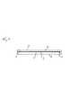
- 複数の分割ラインによって区切られた複数のデバイスを備えたデバイス領域(2)と、前記デバイス領域(2)の周りにデバイスが形成されない周辺限界領域(3)とを一面(1)に有するウェハ(W)をダイに分割する方法であって、
前記ウェハ(W)の前記一面(1)に前記ウェハ上のデバイスを保護する為の接着テープ(4)を付けるステップであって、前記接着テープ(4)が全部のデバイスに接着する、ステップと、
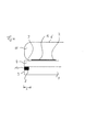
接続手段(10)によって、前記デバイスと接触する前記面の反対側にある前記接着テープ(4)の面に、前記接着テープ(4)を支持する為のキャリア(7)を接続するステップと、
前記ウェハの高さを調整する為に前記一面(1)の反対側にある前記ウェハ(W)の面(6)を研削するステップと、
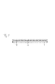
前記分割ラインに沿って前記ウェハ(W)を切断するステップと、
を備え、
前記接続手段(10)は、環状形状を呈し、前記ウェハ(W)の中央部に延びず、
前記ウェハ(W)は、前記ダイが互いに分離されるように完全に分割されることを特徴とする、前記方法。 - 接続手段(10)は、接着特性を呈し、前記接着特性は、エネルギの入力によって取り外し可能であり、前記接続手段(10)は、UV硬化性接着剤、熱硬化性接着剤、それらの組合せを含む、請求項1に記載の方法。
- キャリア(7)および接着テープ(4)の間の接続を解除する為に前記接続手段(10)にエネルギを入力するステップと、
前記キャリア(7)を前記接着テープ(4)から取り除くステップと、
を更に有する、請求項2に記載の方法。 - 前記接続手段(10)の挿入の為に前記キャリア(7)において、凹部を形成する、請求項1〜3のいずれか一項に記載の方法。
- 前記ウェハ(W)の一面(1)が、レーザによって部分的に切断され、前記ウェハの更なる領域が機械的に切断される、請求項1〜4のいずれか一項に記載の方法。
- 前記ウェハの更なる領域が、前記ウェハ(W)の前記一面(1)から、或いは、前記一面(1)の反対側にある前記ウェハ(W)の面(6)から、機械的に切断される、請求項5に記載の方法。
- 前記一面(1)の反対側にある前記ウェハ(W)の面(6)は、部分的に機械的に切断され、前記ウェハ(W)の更なる領域は、前記一面(1)の反対側にある前記ウェハ(W)の前記面(6)からレーザによって切断される、請求項1〜4のいずれか一項に記載の方法。
- 前記ウェハの前記切断は、前記ウェハの研削前に行われる、請求項1〜7のいずれか一項に記載の方法。
- 前記列挙された順序で請求項1に記載のステップが行われる、請求項1〜7のいずれか一項に記載の方法。
- 前記デバイスに接触する表面の反対側にある前記接着テープ(4)の表面は、前記一面(1)の反対側にある前記ウェハ(W)の前記表面と平行にされている、請求項1〜9のいずれか一項に記載の方法。
- 前記ウェハ(W)の研削された表面に接着性ピックアップテープ(11)を付けるステップを更に有する、請求項1〜10のいずれか一項に記載の方法。
- 前記キャリア(7)は、シリコンおよび/またはガラスで形成される、請求項1〜11のいずれか一項に記載の方法。
Applications Claiming Priority (2)
| Application Number | Priority Date | Filing Date | Title |
|---|---|---|---|
| DE102014227005.7 | 2014-12-29 | ||
| DE102014227005.7A DE102014227005B4 (de) | 2014-12-29 | 2014-12-29 | Verfahren zum Aufteilen eines Wafers in Chips |
Publications (2)
| Publication Number | Publication Date |
|---|---|
| JP2016127273A JP2016127273A (ja) | 2016-07-11 |
| JP6233936B2 true JP6233936B2 (ja) | 2017-11-22 |
Family
ID=56116737
Family Applications (1)
| Application Number | Title | Priority Date | Filing Date |
|---|---|---|---|
| JP2015230840A Active JP6233936B2 (ja) | 2014-12-29 | 2015-11-26 | ウェハをダイに分割する方法 |
Country Status (8)
| Country | Link |
|---|---|
| US (1) | US9704749B2 (ja) |
| JP (1) | JP6233936B2 (ja) |
| KR (1) | KR101747561B1 (ja) |
| CN (1) | CN105742212B (ja) |
| DE (1) | DE102014227005B4 (ja) |
| MY (1) | MY175846A (ja) |
| SG (1) | SG10201509836PA (ja) |
| TW (1) | TWI607486B (ja) |
Families Citing this family (4)
| Publication number | Priority date | Publication date | Assignee | Title |
|---|---|---|---|---|
| DE102016112976A1 (de) | 2016-07-14 | 2018-01-18 | Infineon Technologies Ag | Verfahren zum Bearbeiten eines Wafers und Schichtstapel |
| KR102030398B1 (ko) * | 2017-07-28 | 2019-10-10 | (주) 예스티 | 웨이퍼 다이싱 방법 및 웨이퍼를 다이싱하기 위한 시스템 |
| KR102030409B1 (ko) * | 2017-07-28 | 2019-10-10 | (주) 예스티 | 웨이퍼 다이싱 방법 및 웨이퍼를 다이싱하기 위한 시스템 |
| CN117832152A (zh) * | 2023-12-18 | 2024-04-05 | 深圳镁伽科技有限公司 | 调整机构及加工装置 |
Family Cites Families (25)
| Publication number | Priority date | Publication date | Assignee | Title |
|---|---|---|---|---|
| US6294439B1 (en) * | 1997-07-23 | 2001-09-25 | Kabushiki Kaisha Toshiba | Method of dividing a wafer and method of manufacturing a semiconductor device |
| US6184109B1 (en) * | 1997-07-23 | 2001-02-06 | Kabushiki Kaisha Toshiba | Method of dividing a wafer and method of manufacturing a semiconductor device |
| JP2001035817A (ja) * | 1999-07-22 | 2001-02-09 | Toshiba Corp | ウェーハの分割方法及び半導体装置の製造方法 |
| TWI241674B (en) * | 2001-11-30 | 2005-10-11 | Disco Corp | Manufacturing method of semiconductor chip |
| JP3612317B2 (ja) * | 2001-11-30 | 2005-01-19 | 株式会社東芝 | 半導体装置の製造方法 |
| JP2003234455A (ja) * | 2002-02-07 | 2003-08-22 | Matsushita Electric Ind Co Ltd | 電子デバイスの製造方法、電子デバイスおよび電子デバイス装置 |
| JP2004014956A (ja) * | 2002-06-11 | 2004-01-15 | Shinko Electric Ind Co Ltd | 微小半導体素子の加工処理方法 |
| JP4462997B2 (ja) * | 2003-09-26 | 2010-05-12 | 株式会社ディスコ | ウェーハの加工方法 |
| DE20318462U1 (de) * | 2003-11-26 | 2004-03-11 | Infineon Technologies Ag | Anordnung elektronischer Halbleiterbauelemente auf einem Trägersystem zur Behandlung der Halbleiterbauelemente mit einem flüssigen Medium |
| WO2006006611A1 (en) * | 2004-07-09 | 2006-01-19 | Semiconductor Energy Laboratory Co., Ltd. | Ic chip and its manufacturing method |
| JP2008135446A (ja) * | 2006-11-27 | 2008-06-12 | Philtech Inc | Rfパウダーの製造方法 |
| JP2008258282A (ja) * | 2007-04-02 | 2008-10-23 | Toshiba Corp | 半導体ウェハのチップ化方法 |
| CN101809718A (zh) * | 2007-12-20 | 2010-08-18 | 立山机械股份有限公司 | 黏着材的黏着方法及黏着装置 |
| US8043940B2 (en) * | 2008-06-02 | 2011-10-25 | Renesas Electronics Corporation | Method for manufacturing semiconductor chip and semiconductor device |
| JP5308213B2 (ja) * | 2009-03-31 | 2013-10-09 | セミコンダクター・コンポーネンツ・インダストリーズ・リミテッド・ライアビリティ・カンパニー | 半導体装置の製造方法 |
| JP5495647B2 (ja) | 2009-07-17 | 2014-05-21 | 株式会社ディスコ | ウェーハの加工方法 |
| JP2010056562A (ja) * | 2009-11-26 | 2010-03-11 | Nitto Denko Corp | 半導体チップの製造方法 |
| JP2011159679A (ja) * | 2010-01-29 | 2011-08-18 | Furukawa Electric Co Ltd:The | チップの製造方法 |
| US9559004B2 (en) * | 2011-05-12 | 2017-01-31 | STATS ChipPAC Pte. Ltd. | Semiconductor device and method of singulating thin semiconductor wafer on carrier along modified region within non-active region formed by irradiating energy |
| JP2013135038A (ja) * | 2011-12-26 | 2013-07-08 | Elpida Memory Inc | 半導体装置の製造方法 |
| JP2014017462A (ja) * | 2012-03-02 | 2014-01-30 | Fujifilm Corp | 半導体装置の製造方法 |
| US8580655B2 (en) * | 2012-03-02 | 2013-11-12 | Disco Corporation | Processing method for bump-included device wafer |
| JP2014135348A (ja) * | 2013-01-09 | 2014-07-24 | Disco Abrasive Syst Ltd | ウエーハの加工方法 |
| JP6078376B2 (ja) * | 2013-02-22 | 2017-02-08 | 株式会社ディスコ | ウエーハの加工方法 |
| JP2014165388A (ja) * | 2013-02-26 | 2014-09-08 | Renesas Electronics Corp | 半導体装置の製造方法 |
-
2014
- 2014-12-29 DE DE102014227005.7A patent/DE102014227005B4/de active Active
-
2015
- 2015-11-19 MY MYPI2015704202A patent/MY175846A/en unknown
- 2015-11-26 JP JP2015230840A patent/JP6233936B2/ja active Active
- 2015-11-30 SG SG10201509836PA patent/SG10201509836PA/en unknown
- 2015-12-16 US US14/970,756 patent/US9704749B2/en active Active
- 2015-12-18 TW TW104142789A patent/TWI607486B/zh active
- 2015-12-23 KR KR1020150184831A patent/KR101747561B1/ko active Active
- 2015-12-25 CN CN201510993795.5A patent/CN105742212B/zh active Active
Also Published As
| Publication number | Publication date |
|---|---|
| TWI607486B (zh) | 2017-12-01 |
| US20160190010A1 (en) | 2016-06-30 |
| US9704749B2 (en) | 2017-07-11 |
| KR20160080075A (ko) | 2016-07-07 |
| KR101747561B1 (ko) | 2017-06-14 |
| DE102014227005B4 (de) | 2023-09-07 |
| TW201635337A (zh) | 2016-10-01 |
| CN105742212A (zh) | 2016-07-06 |
| JP2016127273A (ja) | 2016-07-11 |
| DE102014227005A1 (de) | 2016-06-30 |
| SG10201509836PA (en) | 2016-07-28 |
| MY175846A (en) | 2020-07-13 |
| CN105742212B (zh) | 2019-08-30 |
Similar Documents
| Publication | Publication Date | Title |
|---|---|---|
| JP6327532B2 (ja) | ウェハ分割方法 | |
| JP6308632B2 (ja) | ウェハを分割する方法 | |
| US10256148B2 (en) | Method of processing wafer | |
| US9905453B2 (en) | Protective sheeting for use in processing a semiconductor-sized wafer and semiconductor-sized wafer processing method | |
| CN109417049B (zh) | 处理背面上具有突出物的晶片的方法 | |
| JP6167984B2 (ja) | ウェーハの加工方法 | |
| JP6233936B2 (ja) | ウェハをダイに分割する方法 | |
| CN101026126A (zh) | 半导体芯片制造方法 | |
| KR102535551B1 (ko) | 피가공물의 연삭 방법 | |
| JP6301658B2 (ja) | ウェーハの加工方法 | |
| KR20060123462A (ko) | 웨이퍼의 전사방법 | |
| JP6125170B2 (ja) | ウェーハの加工方法 | |
| JP2017050443A (ja) | ウエーハの加工方法 | |
| JP2007281001A (ja) | 半導体ウェーハの加工方法 |
Legal Events
| Date | Code | Title | Description |
|---|---|---|---|
| A131 | Notification of reasons for refusal |
Free format text: JAPANESE INTERMEDIATE CODE: A131 Effective date: 20161108 |
|
| A977 | Report on retrieval |
Free format text: JAPANESE INTERMEDIATE CODE: A971007 Effective date: 20161109 |
|
| A601 | Written request for extension of time |
Free format text: JAPANESE INTERMEDIATE CODE: A601 Effective date: 20161222 |
|
| A521 | Request for written amendment filed |
Free format text: JAPANESE INTERMEDIATE CODE: A523 Effective date: 20170307 |
|
| A131 | Notification of reasons for refusal |
Free format text: JAPANESE INTERMEDIATE CODE: A131 Effective date: 20170425 |
|
| A601 | Written request for extension of time |
Free format text: JAPANESE INTERMEDIATE CODE: A601 Effective date: 20170626 |
|
| A521 | Request for written amendment filed |
Free format text: JAPANESE INTERMEDIATE CODE: A523 Effective date: 20170815 |
|
| TRDD | Decision of grant or rejection written | ||
| A01 | Written decision to grant a patent or to grant a registration (utility model) |
Free format text: JAPANESE INTERMEDIATE CODE: A01 Effective date: 20170926 |
|
| A61 | First payment of annual fees (during grant procedure) |
Free format text: JAPANESE INTERMEDIATE CODE: A61 Effective date: 20171020 |
|
| R150 | Certificate of patent or registration of utility model |
Ref document number: 6233936 Country of ref document: JP Free format text: JAPANESE INTERMEDIATE CODE: R150 |
|
| R250 | Receipt of annual fees |
Free format text: JAPANESE INTERMEDIATE CODE: R250 |
|
| R250 | Receipt of annual fees |
Free format text: JAPANESE INTERMEDIATE CODE: R250 |
|
| R250 | Receipt of annual fees |
Free format text: JAPANESE INTERMEDIATE CODE: R250 |
|
| R250 | Receipt of annual fees |
Free format text: JAPANESE INTERMEDIATE CODE: R250 |
|
| R250 | Receipt of annual fees |
Free format text: JAPANESE INTERMEDIATE CODE: R250 |
|
| R250 | Receipt of annual fees |
Free format text: JAPANESE INTERMEDIATE CODE: R250 |