JP6282983B2 - 基板処理装置 - Google Patents
基板処理装置 Download PDFInfo
- Publication number
- JP6282983B2 JP6282983B2 JP2014556152A JP2014556152A JP6282983B2 JP 6282983 B2 JP6282983 B2 JP 6282983B2 JP 2014556152 A JP2014556152 A JP 2014556152A JP 2014556152 A JP2014556152 A JP 2014556152A JP 6282983 B2 JP6282983 B2 JP 6282983B2
- Authority
- JP
- Japan
- Prior art keywords
- substrate
- carrier
- processing apparatus
- substrate processing
- transport
- Prior art date
- Legal status (The legal status is an assumption and is not a legal conclusion. Google has not performed a legal analysis and makes no representation as to the accuracy of the status listed.)
- Active
Links
Images





Classifications
-
- H—ELECTRICITY
- H10—SEMICONDUCTOR DEVICES; ELECTRIC SOLID-STATE DEVICES NOT OTHERWISE PROVIDED FOR
- H10P—GENERIC PROCESSES OR APPARATUS FOR THE MANUFACTURE OR TREATMENT OF DEVICES COVERED BY CLASS H10
- H10P72/00—Handling or holding of wafers, substrates or devices during manufacture or treatment thereof
- H10P72/30—Handling or holding of wafers, substrates or devices during manufacture or treatment thereof for conveying, e.g. between different workstations
- H10P72/32—Handling or holding of wafers, substrates or devices during manufacture or treatment thereof for conveying, e.g. between different workstations between different workstations
- H10P72/3218—Conveying cassettes, containers or carriers
-
- H—ELECTRICITY
- H10—SEMICONDUCTOR DEVICES; ELECTRIC SOLID-STATE DEVICES NOT OTHERWISE PROVIDED FOR
- H10P—GENERIC PROCESSES OR APPARATUS FOR THE MANUFACTURE OR TREATMENT OF DEVICES COVERED BY CLASS H10
- H10P72/00—Handling or holding of wafers, substrates or devices during manufacture or treatment thereof
- H10P72/30—Handling or holding of wafers, substrates or devices during manufacture or treatment thereof for conveying, e.g. between different workstations
- H10P72/33—Handling or holding of wafers, substrates or devices during manufacture or treatment thereof for conveying, e.g. between different workstations into and out of processing chamber
- H10P72/3311—Horizontal transfer of a batch of workpieces
-
- H—ELECTRICITY
- H10—SEMICONDUCTOR DEVICES; ELECTRIC SOLID-STATE DEVICES NOT OTHERWISE PROVIDED FOR
- H10P—GENERIC PROCESSES OR APPARATUS FOR THE MANUFACTURE OR TREATMENT OF DEVICES COVERED BY CLASS H10
- H10P72/00—Handling or holding of wafers, substrates or devices during manufacture or treatment thereof
- H10P72/04—Apparatus for manufacture or treatment
- H10P72/0451—Apparatus for manufacturing or treating in a plurality of work-stations
- H10P72/0464—Apparatus for manufacturing or treating in a plurality of work-stations characterised by the construction of the transfer chamber
-
- H—ELECTRICITY
- H10—SEMICONDUCTOR DEVICES; ELECTRIC SOLID-STATE DEVICES NOT OTHERWISE PROVIDED FOR
- H10P—GENERIC PROCESSES OR APPARATUS FOR THE MANUFACTURE OR TREATMENT OF DEVICES COVERED BY CLASS H10
- H10P72/00—Handling or holding of wafers, substrates or devices during manufacture or treatment thereof
- H10P72/30—Handling or holding of wafers, substrates or devices during manufacture or treatment thereof for conveying, e.g. between different workstations
- H10P72/32—Handling or holding of wafers, substrates or devices during manufacture or treatment thereof for conveying, e.g. between different workstations between different workstations
- H10P72/3211—Changing orientation of the substrate, e.g. from a horizontal position to a vertical position
-
- H—ELECTRICITY
- H10—SEMICONDUCTOR DEVICES; ELECTRIC SOLID-STATE DEVICES NOT OTHERWISE PROVIDED FOR
- H10P—GENERIC PROCESSES OR APPARATUS FOR THE MANUFACTURE OR TREATMENT OF DEVICES COVERED BY CLASS H10
- H10P72/00—Handling or holding of wafers, substrates or devices during manufacture or treatment thereof
- H10P72/30—Handling or holding of wafers, substrates or devices during manufacture or treatment thereof for conveying, e.g. between different workstations
- H10P72/34—Handling or holding of wafers, substrates or devices during manufacture or treatment thereof for conveying, e.g. between different workstations the wafers being stored in a carrier, involving loading and unloading
- H10P72/3411—Handling or holding of wafers, substrates or devices during manufacture or treatment thereof for conveying, e.g. between different workstations the wafers being stored in a carrier, involving loading and unloading involving loading and unloading of wafers
Landscapes
- Container, Conveyance, Adherence, Positioning, Of Wafer (AREA)
Description
Claims (27)
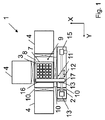
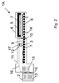
- 基板処理装置(1、1A〜1N)であって、
少なくとも一つの基板(3)がある基板処理装置(1)のローディングとアンローディングのための少なくとも一つの基板ローディングおよびアンローディング領域(2)と、 少なくとも一つの排気可能な処理チャンバ(5)と、
前記少なくとも一つの基板(3)が、前記少なくとも一つの処理チャンバ(5)に向かう少なくとも一つのキャリア搬送領域(9)における少なくとも一つのキャリア搬送装置(8)によって搬送される少なくとも一つのキャリア装置(7)と、
前記基板ローディングおよびアンローディング領域(2)と前記キャリア搬送領域(9)の間の少なくとも一つの気密閉鎖装置(10)と同様の前記少なくとも一つの処理チャンバ(5)と前記キャリア搬送領域(9)の間の少なくとも一つの気密閉鎖装置(10)とを含んで構成されたものにおいて、
前記基板ローディングおよびアンローディング領域(2)が、前記基板ローディングおよびアンローディング領域(2)内で備えることが可能で、基板(3)を基板カセット(13)の異なる水平カセットレベルに配置されることができる少なくとも一つの基板カセット(13)から、前記少なくとも一つの基板(3)が、水平キャリアレベルに保持可能で、基板搬送領域(11)が前記基板ローディングおよびアンローディング領域(2)に対して気密閉鎖可能である、前記少なくとも一つのキャリア装置(7)に搬送するための少なくとも一つの基板搬送装置(12)がある前記基板搬送領域(11)のそばのキャリア搬送領域に結びつけられ、
前記基板搬送装置(12)は、前記キャリア装置(7)の基板キャリア行と平行に配置されて、該キャリア装置(7)の上方にある、搬送アームに個別に対応する搬送ブリッジ(16)を含んで構成されている
ことを特徴とする基板処理装置。 - 前記基板搬送領域(11)が不活性ガスによって充填可能であることを特徴とする請求項1記載の基板処理装置。
- 前記キャリア装置(7)は、基板キャリア行と基板キャリア列内のキャリアレベルに設けられた基板ネストを含んで構成され、前記キャリア装置(7)は、前記基板キャリア行(X)の方向および/または前記基板キャリア列(Y)の方向に移動可能であることを特徴とする請求項1または2に記載の基板処理装置。
- 前記キャリア搬送装置(8)は、ローラ搬送システムを含んで構成されることを特徴とする請求項1から3のいずれか一項に記載の基板処理装置。
- 前記基板搬送装置(12)は、前記キャリア搬送領域(9)の上方で、基板ローディングレベルにあり、基板(3)を行状にまたは列状に装備している前記キャリア装置(7)に対して平行に備えられて構成されることを特徴とする請求項1から4のいずれか一項に記載の基板処理装置。
- 前記基板搬送装置(12)が、少なくとも一つの搬送ブリッジ(16)または搬送アームを含んで構成されており、少なくとも一つの基板(3)を前記キャリア装置(7)の少なくとも一つの基板キャリア行または基板キャリア列にロードし、アンロードするために、この基板キャリア行または基板キャリア列に対して平行に伸長していることを特徴とする請求項1から5のいずれか一項に記載の基板処理装置。
- 前記搬送ブリッジ(16)または、前記キャリア装置(7)のさらに基板キャリア行または基板キャリア列をロードし、アンロードするための転送アームが、基板キャリア列の方向および/または基板キャリア列の方向に沿って移動可動であることを特徴とする請求項6に記載の基板処理装置。
- 前記基板搬送装置(12)は、少なくとも一つの非接触の基板ハンドリング装置(17)を含んで構成されることを特徴とする請求項1から7のいずれか一項に記載の基板処理装置。
- 前記基板ハンドリング装置(17)は、超音波増強型であることを特徴とする請求項8に記載の基板処理装置。
- 前記基板カセット(13)は、前記基板搬送装置(12)によって個別の最上部の基板(3)のアンロードとリターンのためのリフトシステムに結合されていることを特徴とする請求項1から9のいずれか一項に記載の基板処理装置。
- 前記基板処理装置(1)は、少なくとも2つのキャリア装置レベルを含んで構成され、前記キャリア装置レベルにおける前記キャリア装置(7)が独立して移動可能であることを特徴とする請求項1から10のいずれか一項に記載の基板処理装置。
- 前記キャリア装置レベルの少なくとも2つの間で、1つのキャリア装置リフト(28)が設けられ、それによって、少なくとも一つのキャリア装置(7)が別のキャリア装置レベルに持って行くことが可能であることを特徴とする請求項11に記載の基板処理装置。
- 前記基板処理装置(1、1A〜1N)は、互いに上に積み重ねられ、前記キャリア搬送領域(9)と結び付けられている、少なくとも2つの処理チャンバ(5)を含んで構成されることを特徴とする請求項1から12のいずれか一項に記載の基板処理装置。
- 前記基板ローディングおよびアンローディング領域(2)は、カセットストア(19)を含んで構成され、前記カセットストア(19)において少なくとも一つの基板カセット(13)設けられて、基板搬送装置(12)に連結可能となっていることを特徴とする請求項1から13のいずれか一項に記載の基板処理装置。
- 前記カセットストア(19)は、不活性ガスによって排気可能で、および/または充填可能であることを特徴とする請求項14に記載の基板処理装置。
- 前記キャリア搬送領域(9)は、少なくとも一つの調整装置を含んで構成されること
を特徴とする請求項1から15のいずれか一項に記載の基板処理装置。 - 前記基板処理装置(1、1A〜1N)は、基板回転装置を含んで構成されることを特徴とする請求項1から16のいずれか一項に記載の基板処理装置。
- 前記基板回転装置は、基板カセット回転装置(15)であることを特徴とする請求項17に記載の基板処理装置。
- 前記基板処理装置(1、1A〜1N)の少なくとも2つのキャリア搬送領域(9)の間では、一つのキャリア装置(7)から別のキャリア装置(7)の上に少なくとも一つの基板(3)を搬送するための基板搬送ステーション(29)が設けられていることを特徴とする請求項1から18のいずれか一項に記載の基板処理装置。
- 前記基板処理装置(1、1A〜1N)は、基板クラック検出器(20)および/または基板クラック処理装置(21)を含んで構成されることを特徴とする請求項1から19のいずれか一項に記載の基板処理装置。
- 前記処理チャンバ(5)の少なくとも1つは、この処理チャンバ(5)が設けられる処理モジュール(4、6、6´)に対して前記キャリア装置(7)によって物理的に閉鎖可能であることを特徴とする請求項1から20のいずれか一項に記載の基板処理装置。
- 前記キャリア装置(7)が、前記処理チャンバ(5)の底部を形成することを特徴とする請求項21に記載の基板処理装置。
- 前記処理チャンバ(5)は、ガスシャワーとして提供されるHF電極を含んで構成され、それはキャリア装置(7)とともに平行平板配置を形成していることを特徴とする請求項22に記載の基板処理装置。
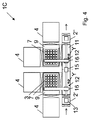
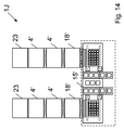
- 前記基板処理装置(1、1A〜1N)は、それぞれ少なくとも一つの処理チャンバ(5)と一緒の少なくとも一つの処理モジュール(4、4´、6、 6´)を含んで構成され、前記少なくとも一つの処理モジュール(4、4´、6、 6´)と前記キャリア搬送領域(9)の間で、搬送モジュール(18、18´、18´´)がそれぞれ備えられ、前記処理モジュール(4、4´、6、 6´)および前記キャリア搬送領域(9)に対して気密に閉鎖可能であることを特徴とする請求項1から23のいずれか一項に記載の基板処理装置。
- 前記搬送モジュール(18、18´、18´´)は、前記キャリア装置(7)のための少なくとも2つのレベルを提供することを特徴とする請求項24に記載の基板処理装置。
- 前記基板処理装置(1、1A〜1N)は、少なくとも一つの処理チャンバ(5)とそれぞれが一緒の少なくとも2つの処理モジュール(4、4´、6、 6´)を含んで構成され、各処理モジュール(4、4´、6、 6´)にそれ自身のキャリア装置(7)が割り当てられていることを特徴とする請求項1から25のいずれか一項に記載の基板処理装置。
- 前記キャリア搬送領域(9)は、前記処理モジュール(4、4´、6、 6´)のための分離領域を形成し、それぞれ異なるキャリア装置(7)上の基板(3)のために交換領域を形成することを特徴とする請求項26に記載の基板処理装置。
Applications Claiming Priority (3)
| Application Number | Priority Date | Filing Date | Title |
|---|---|---|---|
| DE102012100929.5 | 2012-02-06 | ||
| DE102012100929A DE102012100929A1 (de) | 2012-02-06 | 2012-02-06 | Substratbearbeitungsanlage |
| PCT/IB2013/050414 WO2013118003A1 (de) | 2012-02-06 | 2013-01-17 | Substratbearbeitungsanlage |
Publications (2)
| Publication Number | Publication Date |
|---|---|
| JP2015512152A JP2015512152A (ja) | 2015-04-23 |
| JP6282983B2 true JP6282983B2 (ja) | 2018-02-21 |
Family
ID=47884424
Family Applications (1)
| Application Number | Title | Priority Date | Filing Date |
|---|---|---|---|
| JP2014556152A Active JP6282983B2 (ja) | 2012-02-06 | 2013-01-17 | 基板処理装置 |
Country Status (12)
| Country | Link |
|---|---|
| US (1) | US10199250B2 (ja) |
| EP (2) | EP3916764B1 (ja) |
| JP (1) | JP6282983B2 (ja) |
| KR (1) | KR102033694B1 (ja) |
| CN (1) | CN104115264B (ja) |
| DE (1) | DE102012100929A1 (ja) |
| ES (1) | ES2882593T3 (ja) |
| HU (1) | HUE055426T2 (ja) |
| PL (1) | PL2812915T3 (ja) |
| PT (1) | PT2812915T (ja) |
| TW (1) | TWI512878B (ja) |
| WO (1) | WO2013118003A1 (ja) |
Families Citing this family (8)
| Publication number | Priority date | Publication date | Assignee | Title |
|---|---|---|---|---|
| CN106531679B (zh) * | 2015-09-10 | 2019-10-08 | 北京北方华创微电子装备有限公司 | 承载装置及反应腔室 |
| TWI633644B (zh) * | 2017-08-17 | 2018-08-21 | Siliconware Precision Industries Co., Ltd. | 打印設備 |
| DE102018123523A1 (de) * | 2018-09-25 | 2020-03-26 | Meyer Burger (Germany) Gmbh | Prozessmodul und Anlage mit wenigstens einem solchen Prozessmodul |
| CN112582498A (zh) * | 2019-09-30 | 2021-03-30 | 中国电子科技集团公司第四十八研究所 | 一种连续式生产晶体硅太阳能电池的方法 |
| CN113130345B (zh) * | 2019-12-31 | 2023-12-08 | 中微半导体设备(上海)股份有限公司 | 基片处理系统及其维护方法 |
| CN111063768A (zh) * | 2020-01-07 | 2020-04-24 | 晶澳太阳能有限公司 | 一种maia下载仓供气装置 |
| CN116848629A (zh) * | 2021-02-17 | 2023-10-03 | 应用材料公司 | 用于支持多个半导体处理模块或腔室的模块化主机布局 |
| DE102023128552A1 (de) * | 2023-10-18 | 2025-04-24 | Aixtron Se | Be- und Entladezyklus für ein CVD-Reaktorsystem |
Family Cites Families (36)
| Publication number | Priority date | Publication date | Assignee | Title |
|---|---|---|---|---|
| JPH0731539Y2 (ja) * | 1989-02-15 | 1995-07-19 | 富士通株式会社 | 基板処理装置 |
| JP2644912B2 (ja) | 1990-08-29 | 1997-08-25 | 株式会社日立製作所 | 真空処理装置及びその運転方法 |
| JPH04154145A (ja) * | 1990-10-18 | 1992-05-27 | Fuji Electric Co Ltd | 半導体ウェハ処理装置 |
| JP3965343B2 (ja) * | 1994-08-19 | 2007-08-29 | 東京エレクトロン株式会社 | 処理装置 |
| JPH08213446A (ja) * | 1994-12-08 | 1996-08-20 | Tokyo Electron Ltd | 処理装置 |
| US6308818B1 (en) * | 1999-08-02 | 2001-10-30 | Asyst Technologies, Inc. | Transport system with integrated transport carrier and directors |
| JP2001135704A (ja) | 1999-11-09 | 2001-05-18 | Sharp Corp | 基板処理装置及び基板搬送用トレイの搬送制御方法 |
| JP4753224B2 (ja) * | 2000-08-22 | 2011-08-24 | 日本エー・エス・エム株式会社 | ガスラインシステム |
| US6630053B2 (en) | 2000-08-22 | 2003-10-07 | Asm Japan K.K. | Semiconductor processing module and apparatus |
| JP2002141398A (ja) * | 2000-11-02 | 2002-05-17 | Kobe Steel Ltd | 表面処理装置および表面処理方法 |
| JP2002261146A (ja) | 2001-03-02 | 2002-09-13 | Hitachi Ltd | 半導体集積回路装置の製造方法および半導体製造装置 |
| JP2002332570A (ja) * | 2001-05-08 | 2002-11-22 | Anelva Corp | 基板処理装置 |
| JP2003142393A (ja) | 2001-11-07 | 2003-05-16 | Tokyo Seimitsu Co Ltd | 電子ビーム露光装置 |
| CN1293621C (zh) * | 2002-05-23 | 2007-01-03 | 安内华株式会社 | 基板处理装置及处理方法 |
| JP2004018215A (ja) * | 2002-06-18 | 2004-01-22 | Tokyo Electron Ltd | フラット・パネル・ディスプレイ用熱処理装置及び熱処理方法 |
| JP4245387B2 (ja) * | 2003-03-19 | 2009-03-25 | 東京エレクトロン株式会社 | 基板搬送装置及び基板処理装置 |
| JP2004349503A (ja) * | 2003-05-22 | 2004-12-09 | Tokyo Electron Ltd | 被処理体の処理システム及び処理方法 |
| JP2005142200A (ja) | 2003-11-04 | 2005-06-02 | Sharp Corp | 気相成長装置および気相成長方法 |
| US20070269297A1 (en) * | 2003-11-10 | 2007-11-22 | Meulen Peter V D | Semiconductor wafer handling and transport |
| JP4376737B2 (ja) * | 2004-08-31 | 2009-12-02 | 学校法人東京理科大学 | 非接触チャック |
| US20070031609A1 (en) * | 2005-07-29 | 2007-02-08 | Ajay Kumar | Chemical vapor deposition chamber with dual frequency bias and method for manufacturing a photomask using the same |
| JP5330721B2 (ja) | 2007-10-23 | 2013-10-30 | オルボテック エルティ ソラー,エルエルシー | 処理装置および処理方法 |
| JP4997141B2 (ja) * | 2008-02-21 | 2012-08-08 | 株式会社アルバック | 真空処理装置、基板の温度制御方法 |
| WO2010042577A2 (en) * | 2008-10-07 | 2010-04-15 | Applied Materials, Inc. | Advanced platform for processing crystalline silicon solar cells |
| JP2010109089A (ja) * | 2008-10-29 | 2010-05-13 | Kyocera Corp | 搬送装置および成膜基板の製造方法 |
| US8246284B2 (en) * | 2009-03-05 | 2012-08-21 | Applied Materials, Inc. | Stacked load-lock apparatus and method for high throughput solar cell manufacturing |
| IT1394811B1 (it) | 2009-07-08 | 2012-07-13 | Applied Materials Inc | Apparato e procedimento per la manipolazione di substrati danneggiati in sistemi di lavorazione substrati |
| JP5402542B2 (ja) | 2009-11-06 | 2014-01-29 | 村田機械株式会社 | 非接触保持装置及び移載装置 |
| TWI436831B (zh) * | 2009-12-10 | 2014-05-11 | 沃博提克Lt太陽公司 | 真空處理裝置之噴灑頭總成 |
| US20110245957A1 (en) * | 2010-04-06 | 2011-10-06 | Applied Materials, Inc. | Advanced platform for processing crystalline silicon solar cells |
| DE102010016512A1 (de) * | 2010-04-19 | 2011-10-20 | Roth & Rau Ag | Mehrtagen-Rollenofen |
| JP5452349B2 (ja) * | 2010-05-11 | 2014-03-26 | 東京エレクトロン株式会社 | 被処理体の搬送方法、被処理体の搬送装置、及び、プログラム |
| WO2011148924A1 (ja) | 2010-05-24 | 2011-12-01 | 株式会社アルバック | 成膜装置 |
| KR101329303B1 (ko) * | 2010-06-17 | 2013-11-20 | 세메스 주식회사 | 기판들의 로딩 및 언로딩을 위한 기판 처리 장치 |
| DE102010017497A1 (de) * | 2010-06-21 | 2011-12-22 | Roth & Rau Ag | Vorrichtung und Verfahren zum Be-und Entladen von Substratträgerarrays |
| US20130108406A1 (en) * | 2011-11-02 | 2013-05-02 | Varian Semiconductor Equipment Associates, Inc. | High-throughput workpiece handling |
-
2012
- 2012-02-06 DE DE102012100929A patent/DE102012100929A1/de not_active Ceased
-
2013
- 2013-01-17 US US14/376,913 patent/US10199250B2/en active Active
- 2013-01-17 ES ES13709538T patent/ES2882593T3/es active Active
- 2013-01-17 KR KR1020147023259A patent/KR102033694B1/ko active Active
- 2013-01-17 PT PT137095386T patent/PT2812915T/pt unknown
- 2013-01-17 EP EP21177601.8A patent/EP3916764B1/de active Active
- 2013-01-17 HU HUE13709538A patent/HUE055426T2/hu unknown
- 2013-01-17 PL PL13709538T patent/PL2812915T3/pl unknown
- 2013-01-17 CN CN201380008076.2A patent/CN104115264B/zh active Active
- 2013-01-17 WO PCT/IB2013/050414 patent/WO2013118003A1/de not_active Ceased
- 2013-01-17 JP JP2014556152A patent/JP6282983B2/ja active Active
- 2013-01-17 EP EP13709538.6A patent/EP2812915B1/de active Active
- 2013-01-24 TW TW102102646A patent/TWI512878B/zh active
Also Published As
| Publication number | Publication date |
|---|---|
| TW201349374A (zh) | 2013-12-01 |
| WO2013118003A1 (de) | 2013-08-15 |
| TWI512878B (zh) | 2015-12-11 |
| KR102033694B1 (ko) | 2019-10-17 |
| CN104115264B (zh) | 2017-03-22 |
| JP2015512152A (ja) | 2015-04-23 |
| US20140369791A1 (en) | 2014-12-18 |
| EP2812915A1 (de) | 2014-12-17 |
| EP2812915B1 (de) | 2021-07-07 |
| KR20140129038A (ko) | 2014-11-06 |
| US10199250B2 (en) | 2019-02-05 |
| PT2812915T (pt) | 2021-08-19 |
| DE102012100929A1 (de) | 2013-08-08 |
| HUE055426T2 (hu) | 2021-11-29 |
| ES2882593T3 (es) | 2021-12-02 |
| PL2812915T3 (pl) | 2021-11-22 |
| CN104115264A (zh) | 2014-10-22 |
| EP3916764A1 (de) | 2021-12-01 |
| EP3916764B1 (de) | 2022-09-14 |
Similar Documents
| Publication | Publication Date | Title |
|---|---|---|
| JP2015512152A (ja) | 基板処理装置 | |
| US9349620B2 (en) | Apparatus and method for pre-baking substrate upstream of process chamber | |
| US8524004B2 (en) | Loadlock batch ozone cure | |
| JP4237939B2 (ja) | 基板加熱冷却を改良した真空処理装置 | |
| US8367565B2 (en) | Methods and systems of transferring, docking and processing substrates | |
| JP5024179B2 (ja) | 真空装置の動作方法 | |
| CN106449471A (zh) | 衬底处理装置 | |
| US20190013216A1 (en) | Semiconductor device manufacturing platform with single and twinned processing chambers | |
| JP2011049507A (ja) | ロードロック装置及び処理システム | |
| US10854497B2 (en) | Apparatus and method of selective turning over a row of substrates in an array of substrates in a processing system | |
| JP3629371B2 (ja) | 成膜装置および成膜方法 | |
| JP2001135704A (ja) | 基板処理装置及び基板搬送用トレイの搬送制御方法 | |
| US20170352562A1 (en) | Dodecadon transfer chamber and processing system having the same | |
| KR101760667B1 (ko) | 고생산성 박막증착이 가능한 원자층 증착 시스템 | |
| TWI700764B (zh) | 裝載鎖定裝置中的基板冷卻方法、基板搬運方法及裝載鎖定裝置 | |
| CN206742216U (zh) | 基板传送装置及包含该基板传送装置的基板处理系统 | |
| TWI673815B (zh) | 基板處理系統、基板傳送裝置和傳送方法 | |
| JP2014515875A (ja) | マルチチャンバー太陽電池モジュール処理システム及び方法 | |
| WO2010013333A1 (ja) | 真空装置及び真空処理方法 | |
| JP2010135505A (ja) | 真空装置 | |
| US20060156982A1 (en) | Apparatus for fabricating semiconductor device | |
| KR20110016642A (ko) | 기판처리장치 | |
| JP2015137415A (ja) | 大面積原子層蒸着装置 | |
| JP2011204735A (ja) | 基板処理装置および半導体装置の製造方法 | |
| WO2025260379A1 (zh) | 镀膜装置 |
Legal Events
| Date | Code | Title | Description |
|---|---|---|---|
| A621 | Written request for application examination |
Free format text: JAPANESE INTERMEDIATE CODE: A621 Effective date: 20151204 |
|
| A521 | Request for written amendment filed |
Free format text: JAPANESE INTERMEDIATE CODE: A523 Effective date: 20160204 |
|
| A977 | Report on retrieval |
Free format text: JAPANESE INTERMEDIATE CODE: A971007 Effective date: 20161222 |
|
| A131 | Notification of reasons for refusal |
Free format text: JAPANESE INTERMEDIATE CODE: A131 Effective date: 20170110 |
|
| A521 | Request for written amendment filed |
Free format text: JAPANESE INTERMEDIATE CODE: A523 Effective date: 20170407 |
|
| A131 | Notification of reasons for refusal |
Free format text: JAPANESE INTERMEDIATE CODE: A131 Effective date: 20170620 |
|
| A601 | Written request for extension of time |
Free format text: JAPANESE INTERMEDIATE CODE: A601 Effective date: 20170919 |
|
| A521 | Request for written amendment filed |
Free format text: JAPANESE INTERMEDIATE CODE: A523 Effective date: 20171120 |
|
| TRDD | Decision of grant or rejection written | ||
| A01 | Written decision to grant a patent or to grant a registration (utility model) |
Free format text: JAPANESE INTERMEDIATE CODE: A01 Effective date: 20171226 |
|
| A61 | First payment of annual fees (during grant procedure) |
Free format text: JAPANESE INTERMEDIATE CODE: A61 Effective date: 20180125 |
|
| R150 | Certificate of patent or registration of utility model |
Ref document number: 6282983 Country of ref document: JP Free format text: JAPANESE INTERMEDIATE CODE: R150 |
|
| R250 | Receipt of annual fees |
Free format text: JAPANESE INTERMEDIATE CODE: R250 |
|
| R250 | Receipt of annual fees |
Free format text: JAPANESE INTERMEDIATE CODE: R250 |
|
| R250 | Receipt of annual fees |
Free format text: JAPANESE INTERMEDIATE CODE: R250 |
|
| R250 | Receipt of annual fees |
Free format text: JAPANESE INTERMEDIATE CODE: R250 |
|
| R250 | Receipt of annual fees |
Free format text: JAPANESE INTERMEDIATE CODE: R250 |
|
| R250 | Receipt of annual fees |
Free format text: JAPANESE INTERMEDIATE CODE: R250 |