JP6285100B2 - 蛍光体および発光装置 - Google Patents
蛍光体および発光装置 Download PDFInfo
- Publication number
- JP6285100B2 JP6285100B2 JP2013033690A JP2013033690A JP6285100B2 JP 6285100 B2 JP6285100 B2 JP 6285100B2 JP 2013033690 A JP2013033690 A JP 2013033690A JP 2013033690 A JP2013033690 A JP 2013033690A JP 6285100 B2 JP6285100 B2 JP 6285100B2
- Authority
- JP
- Japan
- Prior art keywords
- phosphor
- light emitting
- light
- emission
- peak intensity
- Prior art date
- Legal status (The legal status is an assumption and is not a legal conclusion. Google has not performed a legal analysis and makes no representation as to the accuracy of the status listed.)
- Expired - Fee Related
Links
Images


Classifications
-
- C—CHEMISTRY; METALLURGY
- C09—DYES; PAINTS; POLISHES; NATURAL RESINS; ADHESIVES; COMPOSITIONS NOT OTHERWISE PROVIDED FOR; APPLICATIONS OF MATERIALS NOT OTHERWISE PROVIDED FOR
- C09K—MATERIALS FOR MISCELLANEOUS APPLICATIONS, NOT PROVIDED FOR ELSEWHERE
- C09K11/00—Luminescent materials, e.g. electroluminescent or chemiluminescent
- C09K11/08—Luminescent materials, e.g. electroluminescent or chemiluminescent containing inorganic luminescent materials
- C09K11/77—Luminescent materials, e.g. electroluminescent or chemiluminescent containing inorganic luminescent materials containing rare earth metals
- C09K11/7728—Luminescent materials, e.g. electroluminescent or chemiluminescent containing inorganic luminescent materials containing rare earth metals containing europium
-
- C—CHEMISTRY; METALLURGY
- C09—DYES; PAINTS; POLISHES; NATURAL RESINS; ADHESIVES; COMPOSITIONS NOT OTHERWISE PROVIDED FOR; APPLICATIONS OF MATERIALS NOT OTHERWISE PROVIDED FOR
- C09K—MATERIALS FOR MISCELLANEOUS APPLICATIONS, NOT PROVIDED FOR ELSEWHERE
- C09K11/00—Luminescent materials, e.g. electroluminescent or chemiluminescent
- C09K11/08—Luminescent materials, e.g. electroluminescent or chemiluminescent containing inorganic luminescent materials
- C09K11/0883—Arsenides; Nitrides; Phosphides
-
- C—CHEMISTRY; METALLURGY
- C09—DYES; PAINTS; POLISHES; NATURAL RESINS; ADHESIVES; COMPOSITIONS NOT OTHERWISE PROVIDED FOR; APPLICATIONS OF MATERIALS NOT OTHERWISE PROVIDED FOR
- C09K—MATERIALS FOR MISCELLANEOUS APPLICATIONS, NOT PROVIDED FOR ELSEWHERE
- C09K11/00—Luminescent materials, e.g. electroluminescent or chemiluminescent
- C09K11/08—Luminescent materials, e.g. electroluminescent or chemiluminescent containing inorganic luminescent materials
- C09K11/77—Luminescent materials, e.g. electroluminescent or chemiluminescent containing inorganic luminescent materials containing rare earth metals
- C09K11/7728—Luminescent materials, e.g. electroluminescent or chemiluminescent containing inorganic luminescent materials containing rare earth metals containing europium
- C09K11/77348—Silicon Aluminium Nitrides or Silicon Aluminium Oxynitrides
-
- H—ELECTRICITY
- H10—SEMICONDUCTOR DEVICES; ELECTRIC SOLID-STATE DEVICES NOT OTHERWISE PROVIDED FOR
- H10H—INORGANIC LIGHT-EMITTING SEMICONDUCTOR DEVICES HAVING POTENTIAL BARRIERS
- H10H20/00—Individual inorganic light-emitting semiconductor devices having potential barriers, e.g. light-emitting diodes [LED]
- H10H20/80—Constructional details
- H10H20/85—Packages
- H10H20/851—Wavelength conversion means
- H10H20/8511—Wavelength conversion means characterised by their material, e.g. binder
- H10H20/8512—Wavelength conversion materials
- H10H20/8513—Wavelength conversion materials having two or more wavelength conversion materials
-
- H—ELECTRICITY
- H10—SEMICONDUCTOR DEVICES; ELECTRIC SOLID-STATE DEVICES NOT OTHERWISE PROVIDED FOR
- H10H—INORGANIC LIGHT-EMITTING SEMICONDUCTOR DEVICES HAVING POTENTIAL BARRIERS
- H10H20/00—Individual inorganic light-emitting semiconductor devices having potential barriers, e.g. light-emitting diodes [LED]
- H10H20/80—Constructional details
- H10H20/85—Packages
- H10H20/851—Wavelength conversion means
- H10H20/8515—Wavelength conversion means not being in contact with the bodies
-
- H—ELECTRICITY
- H10—SEMICONDUCTOR DEVICES; ELECTRIC SOLID-STATE DEVICES NOT OTHERWISE PROVIDED FOR
- H10H—INORGANIC LIGHT-EMITTING SEMICONDUCTOR DEVICES HAVING POTENTIAL BARRIERS
- H10H20/00—Individual inorganic light-emitting semiconductor devices having potential barriers, e.g. light-emitting diodes [LED]
- H10H20/80—Constructional details
- H10H20/85—Packages
- H10H20/858—Means for heat extraction or cooling
- H10H20/8581—Means for heat extraction or cooling characterised by their material
-
- H—ELECTRICITY
- H10—SEMICONDUCTOR DEVICES; ELECTRIC SOLID-STATE DEVICES NOT OTHERWISE PROVIDED FOR
- H10W—GENERIC PACKAGES, INTERCONNECTIONS, CONNECTORS OR OTHER CONSTRUCTIONAL DETAILS OF DEVICES COVERED BY CLASS H10
- H10W72/00—Interconnections or connectors in packages
- H10W72/50—Bond wires
- H10W72/551—Materials of bond wires
- H10W72/552—Materials of bond wires comprising metals or metalloids, e.g. silver
- H10W72/5522—Materials of bond wires comprising metals or metalloids, e.g. silver comprising gold [Au]
-
- H—ELECTRICITY
- H10—SEMICONDUCTOR DEVICES; ELECTRIC SOLID-STATE DEVICES NOT OTHERWISE PROVIDED FOR
- H10W—GENERIC PACKAGES, INTERCONNECTIONS, CONNECTORS OR OTHER CONSTRUCTIONAL DETAILS OF DEVICES COVERED BY CLASS H10
- H10W74/00—Encapsulations, e.g. protective coatings
-
- H—ELECTRICITY
- H10—SEMICONDUCTOR DEVICES; ELECTRIC SOLID-STATE DEVICES NOT OTHERWISE PROVIDED FOR
- H10W—GENERIC PACKAGES, INTERCONNECTIONS, CONNECTORS OR OTHER CONSTRUCTIONAL DETAILS OF DEVICES COVERED BY CLASS H10
- H10W90/00—Package configurations
- H10W90/701—Package configurations characterised by the relative positions of pads or connectors relative to package parts
- H10W90/751—Package configurations characterised by the relative positions of pads or connectors relative to package parts of bond wires
- H10W90/756—Package configurations characterised by the relative positions of pads or connectors relative to package parts of bond wires between a chip and a stacked lead frame, conducting package substrate or heat sink
Landscapes
- Chemical & Material Sciences (AREA)
- Inorganic Chemistry (AREA)
- Engineering & Computer Science (AREA)
- Materials Engineering (AREA)
- Organic Chemistry (AREA)
- Luminescent Compositions (AREA)
- Led Device Packages (AREA)
Description
(ここで、MはSrであり、Srの一部はBa,Ca,MgおよびNaから選ばれる少なくとも一種で置換されていてもよい。x,y,z,uおよびwは、それぞれ以下を満たす。
−1.5≦u≦−0.3; −3<u−w≦1)
(ここで、MはSrであり、Srの一部はBa,Ca,MgおよびNaから選ばれる少なくとも一種で置換されていてもよい。x,y,z,uおよびwは、それぞれ以下を満たす。
−1.5≦u≦−0.3; −3<u−w≦1)
上記一般式(1)に示されるように、発光中心元素EuはMの少なくとも一部を置換する。MはSrであり、Srの一部は、Ba、Ca、MgおよびNaから選ばれる少なくとも一種で置換されていてもよい。M全体の15at.%以下、より望ましくは10at.%以下であれば、Ba,Ca、MgおよびNaから選ばれる少なくとも一種が含有されていても、異相の生成が促進されることはない。
本実施形態にかかる蛍光体は、温度が上昇しても発光強度の低下が少ない緑色発光蛍光体である。したがって、図1に示す発光装置は、温度が上昇しても強度の高い緑色発光を発することができる。
まず、Sr原料、Eu原料、Si原料、およびAl原料として、Sr3N2、EuN、Si3N4、Al2O3およびAlNを用意し、バキュームグローブボックス中でそれぞれ秤量した。Sr3N2、EuN、Si3N4、Al2O3およびAlNの配合量は、それぞれ2.830g、0.087g、6.548g、0.340g、および0.547gとした。秤量された原料粉体は、めのう乳鉢内で乾式混合した。
Sr3N2およびEuNの配合量を、それぞれ2.837gおよび0.075gに変更し、めのう乳鉢での解砕工程をはさんだ焼成を7回に変更した以外は実施例1と同様にして実施例2の蛍光体を得た。本実施例の蛍光体の設計組成は(Sr0.985Eu0.015)3Si14Al2ON22である。
Sr3N2およびEuNの配合量を、それぞれ2.823gおよび0.100gに変更し、めのう乳鉢での解砕工程をはさんだ焼成を3回に変更した以外は実施例1と同様にして実施例3の蛍光体を得た。本実施例の蛍光体の設計組成は(Sr0.98Eu0.02)3Si14Al2ON22である。
Sr3N2、EuN、Si3N4、Al2O3およびAlNの配合量を、それぞれ2.852g、0.050g、6.782g、0.170gおよび0.478gに変更し、めのう乳鉢での解砕工程をはさんだ焼成を3回に変更した以外は実施例1と同様にして実施例4の蛍光体を得た。本実施例の蛍光体の設計組成は(Sr0.99Eu0.01)3Si14.5Al1.5O0.5N22.5である。
Sr3N2、EuN、Si3N4、Al2O3およびAlNの配合量を、それぞれ2.866g、0.025g、7.016g、0.000gおよび0.410gに変更した外は実施例1と同様にして実施例5の蛍光体を得た。本実施例の蛍光体の設計組成は(Sr0.995Eu0.005)3Si15AlN23である。
Sr3N2およびEuNの配合量を、それぞれ2.878gおよび0.005gに変更した以外は実施例5と同様にして実施例6の蛍光体を得た。本実施例の蛍光体の設計組成は(Sr0.999Eu0.001)3Si15AlN23である。
Si3N4、Al2O3およびAlNの配合量を、それぞれ6.665g、0.255gおよび0.512gに変更し、めのう乳鉢での解砕工程をはさんだ焼成を6回に変更した以外は実施例1と同様にして実施例7の蛍光体を得た。本実施例の蛍光体の設計組成は(Sr0.985Eu0.015)3Si14.25Al1.75O0.75N22.25である。
Sr3N2およびEuNの配合量を、それぞれ2.837gおよび0.075gに変更した以外は実施例7と同様にして実施例8の蛍光体を得た。本実施例の蛍光体の設計組成は(Sr0.9825Eu0.0175)3Si14.25Al1.75O0.75N22.25である。
Sr3N2およびEuNの配合量を、それぞれ2.837gおよび0.075gに変更し、めのう乳鉢での解砕工程をはさんだ焼成を7回に変更した以外は実施例4と同様にして実施例9の蛍光体を得た。本実施例の蛍光体の設計組成は(Sr0.985Eu0.015)3Si14.25Al1.75O0.5N22.5である。

Si3N4、Al2O3およびAlNの配合量を、それぞれ6.080g、0.680g、0.683gに変更した以外は実施例1と同様にして比較例1の蛍光体を得た。本比較例の蛍光体の設計組成は(Sr0.9825Eu0.0175)3Si13Al3O2N21である。
原料粉体の混合に遊星ボールミルを用いた以外は比較例1と同様にして、比較例2の蛍光体を得た。本比較例の蛍光体の設計組成は(Sr0.9825Eu0.0175)3Si13Al3O2N21である。
Sr3N2およびEuNの配合量を、それぞれ2.837gおよび0.075gに変更した以外は比較例1と同様にして比較例3の蛍光体を得た。本比較例の蛍光体の設計組成は(Sr0.985Eu0.015)3Si13Al3O2N21である。
Sr3N2、EuN、Si3N4およびAlNの配合量を、それぞれ2.878g、0.005g、6.080gおよび0.865gに変更し、めのう乳鉢での解砕工程をはさんだ焼成を3回に変更した以外は比較例1と同様にして比較例4の蛍光体を得た。本比較例の蛍光体の設計組成は(Sr0.999Eu0.001)3Si13Al3N23である。
b:Si/Al=14.25/1.75
c:Si/Al=14.5/1.5
d:Si/Al=15/1
いずれの場合においても、ピーク波長が長くなると強度維持率は低下する傾向にある。しかしながら、Si/Al比が大きくなると、強度維持率はより高い値となり、より優れた温度特性が得られることがわかる。
103…パッケージカップ; 104…反射面; 105…凹部; 106…発光素子
107…ボンディングワイヤー; 108…ボンディングワイヤー; 109…発光層
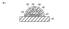
110…蛍光体; 111…樹脂層; 401…絶縁基板 402…発光素子
403…ボンディングワイヤー: 404…透明樹脂層; 405…第一の蛍光層
406…第二の蛍光層; 407…第三の蛍光層。
Claims (8)
- 250〜500nmの波長範囲内に発光ピークを有する光で励起した際に、490〜580nmの波長範囲内に発光ピークを示し、下記一般式(1)で表わされる組成を有し、Cu−Kα線を用いたBragg−Brendano法によるX線回折において、2θ=30.1°〜31.1°に生ずる最大ピークの回折ピーク強度(I31)が2θ=25.0°〜26.0°に生ずる回折ピーク強度(I26)より高く、
前記蛍光体は、2.8以上7.4以下のアスペクト比を有する粒子であることを特徴とする蛍光体。
(M1-xEux)3-yAl3+zSi13-zO2+uN21-w (1)
(ここで、MはSrであり、Srの一部はBa,Ca,MgおよびNaから選ばれる少なくとも一種で置換されていてもよい。x,y,z,uおよびwは、それぞれ以下を満たす。
0<x≦1; −0.1≦y≦0.3; −3≦z≦−0.52
−1.5≦u≦−0.3; −3<u−w≦1) - 前記一般式(1)におけるxは、0.001≦x≦0.5であることを特徴とする請求項1に記載の蛍光体。
- 前記一般式(1)におけるyは、0≦y≦0.25であることを特徴とする請求項1に記載の蛍光体。
- 前記一般式(1)におけるzは、−2≦z≦−0.52であることを特徴とする請求項1に記載の蛍光体。
- 前記一般式(1)におけるuは、−1≦u≦−0.3であることを特徴とする請求項1に記載の蛍光体。
- 前記一般式(1)におけるu−wは、−2≦u−w≦0であることを特徴とする請求項1に記載の蛍光体。
- 前記蛍光体は、5μm以上61μm以下の粒径を有する粒子であることを特徴とする請求項1に記載の蛍光体。
- 250nm〜500nmの波長範囲内に発光ピークを有する光を発する発光素子と、
前記発光素子からの光を受けて発光する蛍光体を含有する発光層とを具備し、
前記蛍光体は、請求項1に記載の蛍光体を含むことを特徴とする発光装置。
Priority Applications (6)
| Application Number | Priority Date | Filing Date | Title |
|---|---|---|---|
| JP2013033690A JP6285100B2 (ja) | 2012-06-13 | 2013-02-22 | 蛍光体および発光装置 |
| US13/837,836 US9022591B2 (en) | 2012-06-13 | 2013-03-15 | Luminescent material |
| EP13160043.9A EP2674470B1 (en) | 2012-06-13 | 2013-03-19 | Luminescent material |
| CN201310232260.7A CN103484119B (zh) | 2012-06-13 | 2013-06-13 | 发光材料 |
| TW102120900A TWI507507B (zh) | 2012-06-13 | 2013-06-13 | 發光材料 |
| KR1020130067536A KR101451016B1 (ko) | 2012-06-13 | 2013-06-13 | 발광 물질 |
Applications Claiming Priority (3)
| Application Number | Priority Date | Filing Date | Title |
|---|---|---|---|
| JP2012133861 | 2012-06-13 | ||
| JP2012133861 | 2012-06-13 | ||
| JP2013033690A JP6285100B2 (ja) | 2012-06-13 | 2013-02-22 | 蛍光体および発光装置 |
Related Child Applications (1)
| Application Number | Title | Priority Date | Filing Date |
|---|---|---|---|
| JP2017035351A Division JP6300973B2 (ja) | 2012-06-13 | 2017-02-27 | 蛍光体の特性評価方法 |
Publications (2)
| Publication Number | Publication Date |
|---|---|
| JP2014015597A JP2014015597A (ja) | 2014-01-30 |
| JP6285100B2 true JP6285100B2 (ja) | 2018-02-28 |
Family
ID=47913123
Family Applications (1)
| Application Number | Title | Priority Date | Filing Date |
|---|---|---|---|
| JP2013033690A Expired - Fee Related JP6285100B2 (ja) | 2012-06-13 | 2013-02-22 | 蛍光体および発光装置 |
Country Status (6)
| Country | Link |
|---|---|
| US (1) | US9022591B2 (ja) |
| EP (1) | EP2674470B1 (ja) |
| JP (1) | JP6285100B2 (ja) |
| KR (1) | KR101451016B1 (ja) |
| CN (1) | CN103484119B (ja) |
| TW (1) | TWI507507B (ja) |
Families Citing this family (4)
| Publication number | Priority date | Publication date | Assignee | Title |
|---|---|---|---|---|
| JP5592602B2 (ja) * | 2008-07-31 | 2014-09-17 | 株式会社東芝 | 蛍光体およびそれを用いた発光装置 |
| WO2011024296A1 (ja) * | 2009-08-28 | 2011-03-03 | 株式会社 東芝 | 蛍光体の製造方法およびそれにより製造された蛍光体 |
| JPWO2013137434A1 (ja) * | 2012-03-16 | 2015-08-03 | 株式会社東芝 | 蛍光体、蛍光体の製造方法および発光装置 |
| JP6782427B2 (ja) * | 2014-10-23 | 2020-11-11 | 三菱ケミカル株式会社 | 蛍光体、発光装置、照明装置及び画像表示装置 |
Family Cites Families (12)
| Publication number | Priority date | Publication date | Assignee | Title |
|---|---|---|---|---|
| JP5578597B2 (ja) | 2007-09-03 | 2014-08-27 | 独立行政法人物質・材料研究機構 | 蛍光体及びその製造方法、並びにそれを用いた発光装置 |
| JP2009076656A (ja) * | 2007-09-20 | 2009-04-09 | Sharp Corp | 発光装置、画像表示装置および液晶ディスプレイ |
| JP5592602B2 (ja) * | 2008-07-31 | 2014-09-17 | 株式会社東芝 | 蛍光体およびそれを用いた発光装置 |
| JP4869317B2 (ja) * | 2008-10-29 | 2012-02-08 | 株式会社東芝 | 赤色蛍光体およびそれを用いた発光装置 |
| JP5641384B2 (ja) | 2008-11-28 | 2014-12-17 | 独立行政法人物質・材料研究機構 | 表示装置用照明装置及び表示装置 |
| WO2011024296A1 (ja) * | 2009-08-28 | 2011-03-03 | 株式会社 東芝 | 蛍光体の製造方法およびそれにより製造された蛍光体 |
| JP5238753B2 (ja) * | 2010-05-31 | 2013-07-17 | 株式会社日立製作所 | 照明装置 |
| WO2012023414A1 (ja) * | 2010-08-19 | 2012-02-23 | 宇部興産株式会社 | 珪窒化物蛍光体用窒化珪素粉末並びにそれを用いたSr3Al3Si13O2N21系蛍光体、β-サイアロン蛍光体及びそれらの製造方法 |
| JP5127965B2 (ja) | 2010-09-02 | 2013-01-23 | 株式会社東芝 | 蛍光体およびそれを用いた発光装置 |
| JP5185421B2 (ja) * | 2010-09-09 | 2013-04-17 | 株式会社東芝 | 赤色発光蛍光体およびそれを用いた発光装置 |
| JP5325959B2 (ja) | 2011-03-09 | 2013-10-23 | 株式会社東芝 | 蛍光体およびそれを用いた発光装置 |
| JP5634352B2 (ja) | 2011-08-24 | 2014-12-03 | 株式会社東芝 | 蛍光体、発光装置および蛍光体の製造方法 |
-
2013
- 2013-02-22 JP JP2013033690A patent/JP6285100B2/ja not_active Expired - Fee Related
- 2013-03-15 US US13/837,836 patent/US9022591B2/en active Active
- 2013-03-19 EP EP13160043.9A patent/EP2674470B1/en not_active Not-in-force
- 2013-06-13 KR KR1020130067536A patent/KR101451016B1/ko not_active Expired - Fee Related
- 2013-06-13 CN CN201310232260.7A patent/CN103484119B/zh not_active Expired - Fee Related
- 2013-06-13 TW TW102120900A patent/TWI507507B/zh not_active IP Right Cessation
Also Published As
| Publication number | Publication date |
|---|---|
| EP2674470A1 (en) | 2013-12-18 |
| KR101451016B1 (ko) | 2014-10-15 |
| TWI507507B (zh) | 2015-11-11 |
| US9022591B2 (en) | 2015-05-05 |
| US20140092600A1 (en) | 2014-04-03 |
| CN103484119B (zh) | 2015-05-06 |
| JP2014015597A (ja) | 2014-01-30 |
| EP2674470B1 (en) | 2014-09-10 |
| TW201410845A (zh) | 2014-03-16 |
| CN103484119A (zh) | 2014-01-01 |
| KR20130139801A (ko) | 2013-12-23 |
Similar Documents
| Publication | Publication Date | Title |
|---|---|---|
| JP5762929B2 (ja) | 蛍光体、発光装置、および蛍光体の製造方法 | |
| JP5634352B2 (ja) | 蛍光体、発光装置および蛍光体の製造方法 | |
| JP5746672B2 (ja) | 蛍光体、発光装置、および蛍光体の製造方法 | |
| JP5727955B2 (ja) | 蛍光体およびその製造方法 | |
| JP6285100B2 (ja) | 蛍光体および発光装置 | |
| JP2015157919A (ja) | 蛍光体、発光装置、および蛍光体の製造方法 | |
| JP2014177592A (ja) | 蛍光体およびそれを用いた発光装置 | |
| JP2015166416A (ja) | 蛍光体、蛍光体の製造方法およびそれを用いた発光装置 | |
| US8957447B2 (en) | Phosphor | |
| JP6300973B2 (ja) | 蛍光体の特性評価方法 | |
| JP2014181260A (ja) | 蛍光体、発光装置、および蛍光体の製造方法 | |
| TWI516570B (zh) | 磷光體及發光裝置 | |
| JP2015187250A (ja) | 蛍光体、その製造方法、およびその蛍光体を用いた発光装置 | |
| JP2016056241A (ja) | 蛍光体、その製造方法、およびその蛍光体を用いた発光装置 | |
| JP2016060844A (ja) | 蛍光体、発光装置、および蛍光体の製造方法 | |
| JP2017036392A (ja) | 蛍光体、発光装置、および蛍光体の製造方法 | |
| JP2016060891A (ja) | 蛍光体、蛍光体の製造方法、およびそれを用いた発光装置 | |
| WO2017051457A1 (ja) | 蛍光体、その製造方法、およびその蛍光体を用いた発光装置 |
Legal Events
| Date | Code | Title | Description |
|---|---|---|---|
| RD04 | Notification of resignation of power of attorney |
Free format text: JAPANESE INTERMEDIATE CODE: A7424 Effective date: 20131219 |
|
| RD04 | Notification of resignation of power of attorney |
Free format text: JAPANESE INTERMEDIATE CODE: A7424 Effective date: 20131226 |
|
| RD04 | Notification of resignation of power of attorney |
Free format text: JAPANESE INTERMEDIATE CODE: A7424 Effective date: 20140109 |
|
| A621 | Written request for application examination |
Free format text: JAPANESE INTERMEDIATE CODE: A621 Effective date: 20150915 |
|
| A977 | Report on retrieval |
Free format text: JAPANESE INTERMEDIATE CODE: A971007 Effective date: 20160527 |
|
| A131 | Notification of reasons for refusal |
Free format text: JAPANESE INTERMEDIATE CODE: A131 Effective date: 20160607 |
|
| A02 | Decision of refusal |
Free format text: JAPANESE INTERMEDIATE CODE: A02 Effective date: 20170110 |
|
| RD03 | Notification of appointment of power of attorney |
Free format text: JAPANESE INTERMEDIATE CODE: A7423 Effective date: 20170316 |
|
| A521 | Request for written amendment filed |
Free format text: JAPANESE INTERMEDIATE CODE: A821 Effective date: 20170316 |
|
| A521 | Request for written amendment filed |
Free format text: JAPANESE INTERMEDIATE CODE: A523 Effective date: 20170410 |
|
| A911 | Transfer to examiner for re-examination before appeal (zenchi) |
Free format text: JAPANESE INTERMEDIATE CODE: A911 Effective date: 20170421 |
|
| A912 | Re-examination (zenchi) completed and case transferred to appeal board |
Free format text: JAPANESE INTERMEDIATE CODE: A912 Effective date: 20170630 |
|
| A711 | Notification of change in applicant |
Free format text: JAPANESE INTERMEDIATE CODE: A711 Effective date: 20171130 |
|
| A521 | Request for written amendment filed |
Free format text: JAPANESE INTERMEDIATE CODE: A821 Effective date: 20171130 |
|
| A61 | First payment of annual fees (during grant procedure) |
Free format text: JAPANESE INTERMEDIATE CODE: A61 Effective date: 20180201 |
|
| R150 | Certificate of patent or registration of utility model |
Ref document number: 6285100 Country of ref document: JP Free format text: JAPANESE INTERMEDIATE CODE: R150 |
|
| R250 | Receipt of annual fees |
Free format text: JAPANESE INTERMEDIATE CODE: R250 |
|
| R250 | Receipt of annual fees |
Free format text: JAPANESE INTERMEDIATE CODE: R250 |
|
| R250 | Receipt of annual fees |
Free format text: JAPANESE INTERMEDIATE CODE: R250 |
|
| LAPS | Cancellation because of no payment of annual fees |