JP6474246B2 - Audio signal processing circuit, in-vehicle audio device, audio component device, electronic equipment - Google Patents
Audio signal processing circuit, in-vehicle audio device, audio component device, electronic equipment Download PDFInfo
- Publication number
- JP6474246B2 JP6474246B2 JP2014248809A JP2014248809A JP6474246B2 JP 6474246 B2 JP6474246 B2 JP 6474246B2 JP 2014248809 A JP2014248809 A JP 2014248809A JP 2014248809 A JP2014248809 A JP 2014248809A JP 6474246 B2 JP6474246 B2 JP 6474246B2
- Authority
- JP
- Japan
- Prior art keywords
- input
- audio signal
- data
- signal processing
- processing circuit
- Prior art date
- Legal status (The legal status is an assumption and is not a legal conclusion. Google has not performed a legal analysis and makes no representation as to the accuracy of the status listed.)
- Active
Links
Images


Classifications
-
- H—ELECTRICITY
- H04—ELECTRIC COMMUNICATION TECHNIQUE
- H04S—STEREOPHONIC SYSTEMS
- H04S7/00—Indicating arrangements; Control arrangements, e.g. balance control
- H04S7/30—Control circuits for electronic adaptation of the sound field
-
- H—ELECTRICITY
- H03—ELECTRONIC CIRCUITRY
- H03H—IMPEDANCE NETWORKS, e.g. RESONANT CIRCUITS; RESONATORS
- H03H17/00—Networks using digital techniques
- H03H17/02—Frequency selective networks
- H03H17/0294—Variable filters; Programmable filters
-
- H—ELECTRICITY
- H03—ELECTRONIC CIRCUITRY
- H03H—IMPEDANCE NETWORKS, e.g. RESONANT CIRCUITS; RESONATORS
- H03H17/00—Networks using digital techniques
- H03H17/02—Frequency selective networks
- H03H17/06—Non-recursive filters
Landscapes
- Physics & Mathematics (AREA)
- Engineering & Computer Science (AREA)
- Acoustics & Sound (AREA)
- Signal Processing (AREA)
- Amplifiers (AREA)
Description
本発明は、オーディオ信号処理回路に関し、特にデジタルフィルタ回路に関する。 The present invention relates to an audio signal processing circuit, and more particularly to a digital filter circuit.
CDプレイヤ、オーディオアンプ、カーステレオ、ポータブルオーディオプレイヤ、ポータブルラジオなどのオーディオ機器、あるいは、スマートホン、タブレットPCなどオーディオ再生機能を備える電子機器には、デジタルのオーディオ信号に、さまざまな信号処理を施すサウンドプロセッサを備える。 Audio devices such as CD players, audio amplifiers, car stereos, portable audio players, and portable radios, or electronic devices having an audio playback function such as smart phones and tablet PCs, perform various signal processing on digital audio signals. A sound processor is provided.
図1は、オーディオシステムの構成例を示すブロック図である。オーディオシステム1rは、デジタル音源2d、アナログ音源2a、DSP(Digital Signal ProcessorまたはDigital Sound Processor)4、パワーアンプ8、電気音響変換素子9を備える。
FIG. 1 is a block diagram illustrating a configuration example of an audio system. The
デジタル音源2dは、デジタルオーディオ信号S1dを生成し、I2S(Inter IC Sound)規格に準拠したシリアルバスを介して、DSP4に出力する。デジタル音源2dは、CD(Compact Disc)プレイヤやDVD(Digital Versatile Disc)プレイヤ、BD(Blu-ray(登録商標) Disc)プレイヤであってもよい。あるいは音源2dは、アナログオーディオ信号をデジタルオーディオ信号に変換するA/Dコンバータを含んでもよい。またアナログ音源2aは、アナログオーディオ信号S1aを出力する。
The
DSP4は、デジタルオーディオ信号S1dあるいはアナログオーディオ信号S1aを受ける。A/Dコンバータ10は、アナログオーディオ信号S1aをデジタルオーディオ信号S2dに変換する。マルチプレクサ(セレクタ)12は、デジタルオーディオ信号S1d、S2dを受け、一方を選択する。デジタル信号処理部20は、マルチプレクサ12が選択したオーディオ信号S3に対して、さまざまなデジタル信号処理を施す。
The DSP 4 receives the digital audio signal S1d or the analog audio signal S1a. The A /
デジタル信号処理としては、イコライジング(EQ)、ゲイン補正(GAIN COMP)、フィルタ(FILTER)、ダイナミックレンジコントロール(DRC)、コンプレッション(COMP)、スケーリング処理(SCALER)、クリップ処理(CLIPPER)、デジタルボリウム制御(VOL)、ステレオ−モノラル変換などのその他の処理(etc.)が例示される。 Digital signal processing includes equalization (EQ), gain correction (GAIN COMP), filter (FILTER), dynamic range control (DRC), compression (COMP), scaling processing (SCALER), clip processing (CLIPPER), digital volume control Other processes (etc.) such as (VOL) and stereo-monaural conversion are exemplified.
デジタル信号処理部20から出力されるデジタルオーディオ信号S4は、図示しないD/Aコンバータによってアナログオーディオ信号S5に変換される。パワーアンプ8は、アナログオーディオ信号S5を増幅し、電気音響変換素子9であるスピーカやヘッドホンを駆動する。パワーアンプ8は、アナログアンプであってもデジタルアンプであってもよい。
The digital audio signal S4 output from the digital
近年、音源のハイレゾ化すなわち高サンプリングレート化、多ビット化が進められており、DSP4においても、ハイレゾ音源への対応が求められている。ハイレゾ音源に対応したDSP4では、高音質化のために、IIR(無限インパルス応答)フィルタではなく、回路面積が大きなFIR(有限インパルス応答)フィルタを実装する場合が多く、これがDSP4の回路面積の増大の一因となっている。また、音源のハイレゾ化、音源の多チャンネル化にともないDSP4の回路規模が膨大となってきている。
In recent years, high-resolution sound sources, that is, high sampling rates and multi-bits have been promoted, and
従来では、DSP4のベンダーは、音源のチャンネル数や要求される音質に応じて、個別にDSP4を設計する必要があり、開発コストが増加、開発期間の長期化という問題が生じていた。 Conventionally, DSP4 vendors have to individually design DSP4 according to the number of sound source channels and the required sound quality, resulting in problems such as an increase in development cost and a prolonged development period.
反対にDSP4のユーザ、すなわちオーディオシステム1rの設計者の立場からすれば、音源のチャンネル数、要求する音質に応じて、ベンダーから提供される複数品番のDSPの中から、適切なひとつを選択する必要があった。
On the other hand, from the standpoint of the DSP4 user, that is, the designer of the
本発明は係る課題に鑑みてなされたものであり、そのある態様の例示的な目的のひとつは、さまざまなチャンネル数、要求される音質レベルに対応可能なオーディオ信号処理回路の提供にある。 SUMMARY OF THE INVENTION The present invention has been made in view of the above-mentioned problems, and one of exemplary objects of an aspect thereof is to provide an audio signal processing circuit that can cope with various numbers of channels and required sound quality levels.
本発明のある態様は、オーディオ信号処理回路に関する。オーディオ信号処理回路は、複数N個(Nは2以上の整数)のFIR(Finite Impulse Response)フィルタと、複数N個のFIRフィルタと対応するN個の第1入力ポートと、複数N個のFIRフィルタと対応するN個の第2入力ポートと、複数N個のFIRフィルタと対応するN個の第1出力ポートと、複数N個のFIRフィルタと対応するN個の第2出力ポートと、を備え、ひとつの半導体基板に集積化される。各FIRフィルタは、第1入力端子と、第2入力端子と、第1出力端子と、第2出力端子と、第1入力端子と第1出力端子の間に直列接続された複数m個(mは2以上の整数)の遅延素子と、m個の遅延素子に設けられた複数のタップのデータに所定の係数を乗算する複数の乗算器と、第2入力端子に入力されたデータおよび複数の乗算器の出力データの加算結果である積和データを第2出力端子から出力する加算回路と、を含む。オーディオ信号処理回路は、i番目(2≦i≦N)のFIRフィルタに関して、(i)その第1入力端子に、(i−1)番目のFIRフィルタの第1出力端子のデータが入力され、かつその第2入力端子に、(i−1)番目のFIRフィルタの第2出力端子のデータが入力される状態と、(ii)その第1入力端子に、i番目の第1入力ポートのデータが入力され、かつその第2入力端子に、i番目の第2入力ポートのデータが入力された状態と、(iii)その第1入力端子に、i番目の第1入力ポートのデータが入力され、かつその第2入力端子にゼロが入力される状態と、が切りかえ可能に構成される。 One embodiment of the present invention relates to an audio signal processing circuit. The audio signal processing circuit includes a plurality of N (N is an integer of 2 or more) FIR (Finite Impulse Response) filters, N first input ports corresponding to the plurality of N FIR filters, and a plurality of N FIR filters. N second input ports corresponding to the filters, N first output ports corresponding to the multiple N FIR filters, and N second output ports corresponding to the multiple N FIR filters. And integrated on a single semiconductor substrate. Each FIR filter includes a first input terminal, a second input terminal, a first output terminal, a second output terminal, and a plurality of m pieces (m that are connected in series between the first input terminal and the first output terminal). Is an integer greater than or equal to 2), a plurality of multipliers for multiplying data of a plurality of taps provided in m delay elements by a predetermined coefficient, data input to the second input terminal, and a plurality of And an adder circuit that outputs product-sum data, which is a result of adding the output data of the multiplier, from a second output terminal. The audio signal processing circuit relates to the i-th (2 ≦ i ≦ N) FIR filter, (i) the data of the first output terminal of the (i−1) -th FIR filter is input to the first input terminal, And (ii) the state in which the data of the second output terminal of the FIR filter is input to the second input terminal, and (ii) the data of the i-th first input port to the first input terminal. And the data of the i-th second input port is input to the second input terminal, and (iii) the data of the i-th first input port is input to the first input terminal. And a state in which zero is input to the second input terminal.
オーディオ信号処理回路を複数個組み合わせることにより、チャンネル数や音質要求に応じて、最適なオーディオシステムを構築できる。 By combining multiple audio signal processing circuits, an optimal audio system can be constructed according to the number of channels and sound quality requirements.
オーディオ信号処理回路は、2〜N番目のFIRフィルタに対応する(N−1)個の第1入力マルチプレクサと、2〜N番目のFIRフィルタに対応する(N−1)個の第2入力マルチプレクサと、をさらに備えてもよい。i(2≦i≦N)番目の第1入力マルチプレクサは、(i−1)番目のFIRフィルタの第1出力端子のデータとi番目の第1入力ポートのデータを受け、一方を選択して、i番目のFIRフィルタの第1入力端子に出力し、i(2≦i≦N)番目の第2入力マルチプレクサは、(i−1)番目のFIRフィルタの第2出力端子のデータとi番目の第2入力ポートのデータを受け、それらの一方またはゼロを、i番目のFIRフィルタの第2入力端子に出力してもよい。
第1、第2入力マルチプレクサを用いることで、FIRフィルタごとに、信号経路を個別に選択できる。
The audio signal processing circuit includes (N−1) first input multiplexers corresponding to the 2nd to Nth FIR filters and (N−1) second input multiplexers corresponding to the 2nd to Nth FIR filters. And may be further provided. The i (2 ≦ i ≦ N) -th first input multiplexer receives the data of the first output terminal of the (i−1) -th FIR filter and the data of the i-th first input port, and selects one of them. Output to the first input terminal of the i th FIR filter, and the i (2 ≦ i ≦ N) second input multiplexer outputs the data of the second output terminal of the (i−1) th FIR filter and the i th The second input port data may be received and one or zero of them may be output to the second input terminal of the i th FIR filter.
By using the first and second input multiplexers, signal paths can be individually selected for each FIR filter.
オーディオ信号処理回路は、(N−1)個の第1入力マルチプレクサおよび(N−1)個の第2入力マルチプレクサを制御するコントローラをさらに備えてもよい。 The audio signal processing circuit may further include a controller that controls the (N−1) first input multiplexers and the (N−1) second input multiplexers.
オーディオ信号処理回路は、1番目のFIRフィルタに対応する1番目の第1入力マルチプレクサをさらに備えてもよい。1番目の第1入力マルチプレクサは、オーディオ信号処理回路内の別の第1回路ブロックからの入力データと、1番目の第1入力ポートのデータと、を受け、一方を選択して1番目のFIRフィルタの第1入力端子に出力してもよい。
この態様によれば、オーディオ信号処理回路内の別の回路ブロックにおいて、FIRフィルタ以外のデジタル処理が行なわれる場合には、その回路ブロックからの信号を、フィルタリングの対象とすることもできる。
The audio signal processing circuit may further include a first first input multiplexer corresponding to the first FIR filter. The first first input multiplexer receives input data from another first circuit block in the audio signal processing circuit and data of the first first input port, and selects one to select the first FIR. You may output to the 1st input terminal of a filter.
According to this aspect, when digital processing other than the FIR filter is performed in another circuit block in the audio signal processing circuit, a signal from the circuit block can be a filtering target.
少なくともひとつのFIRフィルタの第2出力端子のデータは、オーディオ信号処理回路内の別の第2回路ブロックに出力可能であってもよい。
この態様によれば、オーディオ信号処理回路内の別の回路ブロックにおいて、FIRフィルタ以外のデジタル処理が行なわれる場合に、フィルタリング処理後のデータを、その回路ブロックに供給できる。
Data of the second output terminal of at least one FIR filter may be output to another second circuit block in the audio signal processing circuit.
According to this aspect, when digital processing other than the FIR filter is performed in another circuit block in the audio signal processing circuit, the data after filtering processing can be supplied to the circuit block.
オーディオ信号処理回路は、N個の第1入力ポートに対応し、それぞれが対応する第1入力ポートのデータを受けるN個の第1レシーバと、N個の第2入力ポートに対応し、それぞれが対応する第2入力ポートのデータを受けるN個の第2レシーバと、をさらに備えてもよい。 The audio signal processing circuit corresponds to N first input ports, each of which corresponds to N first receivers that receive data of the corresponding first input port, and N second input ports, N second receivers that receive data of corresponding second input ports may be further included.
オーディオ信号処理回路は、N個のFIRフィルタに対応し、それぞれが対応するFIRフィルタの第1出力端子のデータを受け、対応する第1出力ポートに出力する、N個の第1トランスミッタと、N個のFIRフィルタに対応し、それぞれが対応するFIRフィルタの第2出力端子のデータを受け、対応する第2出力ポートに出力する、N個の第2トランスミッタと、をさらに備えてもよい。 The audio signal processing circuit corresponds to N FIR filters, each of which receives data at the first output terminal of the corresponding FIR filter and outputs the data to the corresponding first output port; N number of second transmitters corresponding to the number of FIR filters, each receiving data of the second output terminal of the corresponding FIR filter and outputting the data to the corresponding second output port may be further provided.
本発明の別の態様は、車載用オーディオ装置に関する。車載用オーディオ装置は、上述のいずれかのオーディオ信号処理回路を備える。 Another aspect of the present invention relates to an in-vehicle audio apparatus. The in-vehicle audio apparatus includes any one of the above audio signal processing circuits.
本発明の別の態様は、オーディオコンポーネント装置に関する。オーディオコンポーネント装置は、上述のいずれかのオーディオ信号処理回路を備える。 Another aspect of the present invention relates to an audio component device. The audio component device includes any one of the above-described audio signal processing circuits.
本発明の別の態様は、電子機器に関する。電子機器は、上述のいずれかのオーディオ信号処理回路を備える。 Another embodiment of the present invention relates to an electronic device. The electronic apparatus includes any one of the above-described audio signal processing circuits.
なお、以上の構成要素の任意の組み合わせや本発明の構成要素や表現を、方法、装置、システムなどの間で相互に置換したものもまた、本発明の態様として有効である。 Note that any combination of the above-described constituent elements and the constituent elements and expressions of the present invention replaced with each other among methods, apparatuses, systems, and the like are also effective as an aspect of the present invention.
本発明によれば、さまざまなチャンネル数、要求される音質レベルに対応可能なオーディオ信号処理回路を提供できる。 ADVANTAGE OF THE INVENTION According to this invention, the audio signal processing circuit which can respond to various channel numbers and the required sound quality level can be provided.
以下、本発明を好適な実施の形態をもとに図面を参照しながら説明する。各図面に示される同一または同等の構成要素、部材、処理には、同一の符号を付するものとし、適宜重複した説明は省略する。また、実施の形態は、発明を限定するものではなく例示であって、実施の形態に記述されるすべての特徴やその組み合わせは、必ずしも発明の本質的なものであるとは限らない。 The present invention will be described below based on preferred embodiments with reference to the drawings. The same or equivalent components, members, and processes shown in the drawings are denoted by the same reference numerals, and repeated descriptions are omitted as appropriate. The embodiments do not limit the invention but are exemplifications, and all features and combinations thereof described in the embodiments are not necessarily essential to the invention.
本明細書において、「部材Aが、部材Bと接続された状態」とは、部材Aと部材Bが物理的に直接的に接続される場合のほか、部材Aと部材Bが、電気的な接続状態に影響を及ぼさない他の部材を介して間接的に接続される場合も含む。
同様に、「部材Cが、部材Aと部材Bの間に設けられた状態」とは、部材Aと部材C、あるいは部材Bと部材Cが直接的に接続される場合のほか、電気的な接続状態に影響を及ぼさない他の部材を介して間接的に接続される場合も含む。
In this specification, “the state in which the member A is connected to the member B” means that the member A and the member B are electrically connected in addition to the case where the member A and the member B are physically directly connected. It includes the case of being indirectly connected through another member that does not affect the connection state.
Similarly, “the state in which the member C is provided between the member A and the member B” refers to the case where the member A and the member C or the member B and the member C are directly connected, as well as an electrical condition. It includes the case of being indirectly connected through another member that does not affect the connection state.
図2は、実施の形態に係るオーディオ信号処理回路100のブロック図である。オーディオ信号処理回路100は、複数N個(Nは2以上の整数)のFIRフィルタ106、N個の第1入力ポートINA、N個の第2入力ポートINB、N個の第1レシーバ102A、N個の第2レシーバ102B、(N−1)個の第1入力マルチプレクサ104A、(N−1)個の第2入力マルチプレクサ104B、N個の第1トランスミッタ108A、N個の第2トランスミッタ108B、N個の第1出力ポートOUTA、N個の第2出力ポートOUTBを備え、ひとつの半導体基板に集積化される。本実施の形態では、N=4の場合を説明するが、Nは2以上の任意の整数でありえる。
FIG. 2 is a block diagram of the audio
「集積化」とは、回路の構成要素のすべてが半導体基板上に形成される場合や、回路の主要構成要素が一体集積化される場合が含まれ、回路定数の調節用に一部の抵抗やキャパシタなどが半導体基板の外部に設けられていてもよい。回路を1つのICとして集積化することにより、回路面積を削減することができるとともに、回路素子の特性を均一に保つことができる。 “Integration” includes the case where all of the circuit components are formed on a semiconductor substrate, and the case where the main components of the circuit are integrated, and some resistors are used to adjust circuit constants. And a capacitor may be provided outside the semiconductor substrate. By integrating the circuit as one IC, the circuit area can be reduced and the characteristics of the circuit elements can be kept uniform.
FIRフィルタ106は、第1入力端子IAと、第2入力端子IBと、第1出力端子OAと、第2出力端子OBと、複数m個(mは2以上の整数)の遅延素子d1〜dmと、複数の乗算器K1〜Kmと、加算回路107と、を含む。m個の遅延素子d1〜dmは第1入力端子IAと第1出力端子OAの間に直列接続される。複数の乗算器K1〜Kmは、m個の遅延素子d1〜dmに設けられた対応する複数のタップのデータに所定の係数を乗算する。加算回路107は、第2入力端子IBに入力されたデータおよび複数の乗算器K1〜Kmの出力データの加算結果である積和データを生成し、第2出力端子OBから出力する。
The
i番目(2≦i≦N)のFIRフィルタ106_iに着目する。オーディオ信号処理回路100は、各FIRフィルタ106_iの入力に関して、3つの状態が切りかえ可能に構成される。
Attention is paid to the i-th (2 ≦ i ≦ N)
(i)第1状態φ1
FIRフィルタ106_iの第1入力端子IAに、(i−1)番目のFIRフィルタ106_(i−1)の第1出力端子OAのデータが入力され、かつその第2入力端子IBに、(i−1)番目のFIRフィルタ106_(i−1)の第2出力端子OBのデータが入力される状態
(I) First state φ1
Data of the first output terminal OA of the (i-1) th FIR filter 106_ (i-1) is input to the first input terminal IA of the FIR filter 106_i, and (i− 1) State in which the data of the second output terminal OB of the first FIR filter 106_ (i-1) is input
(ii)第2状態φ2
FIRフィルタ106_iの第1入力端子IAに、i番目の第1入力ポートINAiのデータが入力され、かつその第2入力端子IBに、i番目の第2入力ポートINBiのデータが入力される状態
(Ii) Second state φ2
The data of the i-th first input port INA i is input to the first input terminal IA of the
(iii)第3状態φ3
FIRフィルタ106_iの第1入力端子IAに、i番目の第1入力ポートINAiのデータが入力され、かつその第2入力端子IBにゼロが入力される状態
(Iii) Third state φ3
A state in which data of the i-th first input port INA i is input to the first input terminal IA of the
1番目のFIRフィルタ106_1の入力側は、第2状態φ2または第3状態φ3のいずれかが選択可能であり、第1状態φ1は選択できない。 On the input side of the first FIR filter 106_1, either the second state φ2 or the third state φ3 can be selected, and the first state φ1 cannot be selected.
第1状態φ1〜第3状態φ3を切りかえるために、入力マルチプレクサ104A、104Bが設けられる。 In order to switch the first state φ1 to the third state φ3, input multiplexers 104A and 104B are provided.
i(2≦i≦N)番目の第1入力マルチプレクサ104Aiは、(i−1)番目のFIRフィルタ106_iの第1出力端子OAのデータとi番目の第1入力ポートINAiのデータを受け、一方を選択して、i番目のFIRフィルタ106_iの第1入力端子IAに出力する。
The i (2 ≦ i ≦ N) -th first input multiplexer 104A i receives the data of the first output terminal OA of the (i−1) -
i(2≦i≦N)番目の第2入力マルチプレクサ104Biは、(i−1)番目のFIRフィルタ106_(i−1)の第2出力端子OBのデータとi番目の第2入力ポートIBのデータを受け、それらの一方またはゼロを、i番目のFIRフィルタ106_iの第2入力端子IBに出力する。 The i (2 ≦ i ≦ N) -th second input multiplexer 104B i includes the data of the second output terminal OB of the (i−1) -th FIR filter 106_ (i−1) and the i-th second input port IB. And one or zero of them is output to the second input terminal IB of the i-th FIR filter 106_i.
コントローラ120は、複数の第1入力マルチプレクサ104A、複数の入力マルチプレクサ104B、複数の第1レシーバ102A、複数の第2レシーバ102Bを制御する。たとえばコントローラ120は、マルチプレクサやレシーバそれぞれの状態を指示する制御データを格納するメモリもしくはレジスタと、制御データに応じて第1入力マルチプレクサ104A、第2入力マルチプレクサ104B、第1レシーバ102A、第2レシーバ102Bの状態を制御するデコーダと、を含む。
The
第1レシーバ102Aiは、対応する第1入力ポートINAiのデータを受け、対応する入力マルチプレクサ104Aiに出力する。第2レシーバ102Biは、対応する第2入力ポートINBiのデータを受け、対応するFIRフィルタ106_iの第2入力端子IBに出力する。
The first receiver 102A i receives data of the corresponding first input port INA i, and outputs the corresponding input multiplexers 104A i. The second receiver 102B i receives the data of the corresponding second input port INB i and outputs it to the second input terminal IB of the
また第1トランスミッタ108Aiは、対応するFIRフィルタ106_iの第1出力端子OAのデータを受け、対応する第1出力ポートOUTAiに出力する。また第2トランスミッタ108Biは、対応するFIRフィルタ106_iの第2出力端子OBのデータを受け、対応する第2出力ポートOUTBiに出力する。
The first transmitter 108A i receives data from the first output terminal OA of the
レシーバ102、トランスミッタ108の形式は特に限定されない。後述するように使用において、オーディオ信号処理回路100は複数の個が連結されうるが、チップ間のデータ伝送をパラレル形式で行なう場合、レシーバ102、トランスミッタ108はそれぞれ、ビット毎のバッファを含んでもよい。チップ間のデータ伝送をシリアル形式で行なう場合、レシーバ102はシリアルパラレル変換器で構成でき、トランスミッタ108はパラレルシリアル変換器で構成できる。
The types of the receiver 102 and the transmitter 108 are not particularly limited. In use, as will be described later, a plurality of audio
図3(a)〜(c)は、第1状態φ1〜第3状態φ3を示す等価回路図である。
第1レシーバ102A、第2レシーバ102Bは、イネーブル、ディセーブルが切りかえ可能に構成されてもよい。図3(a)の第1状態φ1では、第1レシーバ102A、第2レシーバ102Bはともにディセーブルとされる。図3(b)の第2状態φ2では、第1レシーバ102A、第2レシーバ102Bはともにイネーブルとされる。図3(c)の第3状態φ3では第1レシーバ102Aはイネーブル、第2レシーバ102Bはディセーブルとされる。不要なレシーバ102をディセーブルとすることで、消費電力を低減できる。
3A to 3C are equivalent circuit diagrams illustrating the first state φ1 to the third state φ3.
The first receiver 102A and the second receiver 102B may be configured to be switchable between enable and disable. In the first state φ1 in FIG. 3A, both the first receiver 102A and the second receiver 102B are disabled. In the second state φ2 in FIG. 3B, both the first receiver 102A and the second receiver 102B are enabled. In the third state φ3 in FIG. 3C, the first receiver 102A is enabled and the second receiver 102B is disabled. Power consumption can be reduced by disabling unnecessary receivers 102.
図2に戻る。FIRフィルタ106の出力側に関しては、3つの状態が切りかえ可能となっている。
(i) 第1状態φx
FIRフィルタ106_iの出力端子OA,OBのデータを、出力ポートOUTA,OUBに出力する状態である。
(ii) 第2状態φy
FIRフィルタ106_iの出力端子OA,OBのデータを、隣接するFIRフィルタ106_(i+1)に供給する状態である。
(iii) 第3状態φz
FIRフィルタ106_iの出力端子OBのデータをフィルタ処理後の最終データとして出力ポートOUTBからチップの外部に出力する状態である。
Returning to FIG. Regarding the output side of the
(I) First state φx
In this state, the data of the output terminals OA and OB of the FIR filter 106_i are output to the output ports OUTA and OUB.
(Ii) Second state φy
In this state, the data of the output terminals OA and OB of the FIR filter 106_i is supplied to the adjacent FIR filter 106_ (i + 1).
(Iii) Third state φz
In this state, the data at the output terminal OB of the FIR filter 106_i is output from the output port OUTB to the outside of the chip as the final data after the filtering process.
第1状態φx〜第3状態φzを切りかえるために、第1トランスミッタ108A、第2トランスミッタ108Bそれぞれも、イネーブル、ディセーブルが切りかえ可能に構成される。i番目のトランスミッタ108Aiに関して、対応するFIRフィルタ106_iの第1出力端子OAのデータをOUTAiからチップ外部に出力する場合には、イネーブル、対応するFIRフィルタ106_iの第1出力端子OAのデータを隣のFIRフィルタ106_(i+1)に供給する場合には、ディセーブルとする。i番目のトランスミッタ108Biに関して、対応するFIRフィルタ106_iの第2出力端子OBのデータをOUTBiからチップ外部に出力する場合には、イネーブル、対応するFIRフィルタ106_iの第2出力端子OBのデータを隣のFIRフィルタ106_(i+1)に供給する場合には、ディセーブルとする。 In order to switch from the first state φx to the third state φz, each of the first transmitter 108A and the second transmitter 108B is configured to be enabled and disabled. When the data of the first output terminal OA of the corresponding FIR filter 106_i is output from the chip OUTA i to the outside of the chip for the i-th transmitter 108A i , the data of the first output terminal OA of the corresponding FIR filter 106_i is enabled. When supplying to the adjacent FIR filter 106_ (i + 1), it is disabled. When the data of the second output terminal OB of the corresponding FIR filter 106_i is output from the OUTB i to the outside of the chip for the i-th transmitter 108B i , the data of the second output terminal OB of the corresponding FIR filter 106_i is enabled. When supplying to the adjacent FIR filter 106_ (i + 1), it is disabled.
したがって第1状態φxでは、第1トランスミッタ108Ai、第2トランスミッタ108Biの両方がイネーブルとされる。第2状態φyでは、第1トランスミッタ108Ai、第2トランスミッタ108Biが両方、ディセーブルされる。第3状態φzでは、第1トランスミッタ108Aiがディセーブル、第2トランスミッタ108Biがイネーブルされる。不要なトランスミッタをディセーブルとすることで、消費電力を低減できる。 Therefore, in the first state φx, both the first transmitter 108A i and the second transmitter 108B i are enabled. In the second state φy, both the first transmitter 108A i and the second transmitter 108B i are disabled. In the third state φz, the first transmitter 108A i is disabled and the second transmitter 108B i is enabled. Power consumption can be reduced by disabling unnecessary transmitters.
オーディオデータのビット数について説明する。フィルタリング処理の演算途中におけるオーバーフローやアンダーフローを防止するために、FIRフィルタ106の内部のビット幅は、オーディオデータのビット幅よりも多く設計される。FIRフィルタ106_iの第2出力端子OBのデータに関しては、FIRフィルタの最終出力データとする場合には、オーディオデータのビット幅に丸めて出力され、別のFIRフィルタに入力される中間データとして利用される場合には、多いビット幅のまま出力される。
The number of bits of audio data will be described. In order to prevent overflow or underflow during the filtering processing, the bit width inside the
以上がオーディオ信号処理回路100の構成である。続いてその使用形態を説明する。
図4(a)〜(c)は、オーディオ信号処理回路100の使用形態を示す図である。図4(a)〜(c)では、レシーバ102、入力マルチプレクサ104、トランスミッタ108は省略される。FIRフィルタ106に示される数字は、FIRフィルタ106のタップ数mである。また第1入力ポートINA、第2入力ポートINBのペアは、まとめてINとして示され、第1出力ポートOUTA、第2出力ポートOUTBのペアは、まとめてOUTBとして示す。
The above is the configuration of the audio
4A to 4C are diagrams illustrating usage patterns of the audio
図4(a)〜(c)では、3個のオーディオ信号処理回路100が同時に使用される。
4A to 4C, three audio
図4(a)を参照する。この利用形態では、4チャンネルCH1〜CH4のオーディオ信号それぞれが、3個のFIRフィルタが直列接続されてなる1536タップのFIRフィルタにより処理される。具体的には、オーディオ信号処理回路100_1〜100_3それぞれの1番目のFIRフィルタ106_1が3個直列に接続され、第1チャンネルCH1のオーディオ信号が処理される。同様に、2番目のFIRフィルタ106_2が3個直列に接続され、第2チャンネルCH2のオーディオ信号が処理される。第3チャンネルCH3、第4チャンネルCH4も同様である。 Reference is made to FIG. In this usage mode, each of the audio signals of the four channels CH1 to CH4 is processed by a 1536 tap FIR filter in which three FIR filters are connected in series. Specifically, three first FIR filters 106_1 of each of the audio signal processing circuits 100_1 to 100_3 are connected in series, and the audio signal of the first channel CH1 is processed. Similarly, three second FIR filters 106_2 are connected in series, and the audio signal of the second channel CH2 is processed. The same applies to the third channel CH3 and the fourth channel CH4.
図4(b)を参照する。この利用形態では、2チャンネルCH1,CH2のオーディオ信号それぞれが、6個のFIRフィルタが直列に接続されてなる3072タップのFIRフィルタにより処理される。具体的には、オーディオ信号処理回路100_1〜100_3それぞれの2個のFIRフィルタ106_1、106_2の6個直列に接続され、第1チャンネルCH1のオーディオ信号が処理される。同様に、オーディオ信号処理回路100_1〜100_3それぞれの2個のFIRフィルタ106_3、106_4の6個直列に接続され、第2チャンネルCH2のオーディオ信号が処理される。 Reference is made to FIG. In this usage mode, each of the audio signals of the two channels CH1 and CH2 is processed by a 3072 tap FIR filter in which six FIR filters are connected in series. Specifically, six FIR filters 106_1 and 106_2 of each of the audio signal processing circuits 100_1 to 100_3 are connected in series, and the audio signal of the first channel CH1 is processed. Similarly, six FIR filters 106_3 and 106_4 of each of the audio signal processing circuits 100_1 to 100_3 are connected in series, and the audio signal of the second channel CH2 is processed.
図4(c)を参照する。この利用形態では、1チャンネルCH1のオーディオ信号が、12個のFIRフィルタが直列に接続されてなる6144タップのFIRフィルタにより処理される。 Reference is made to FIG. In this usage mode, an audio signal of one channel CH1 is processed by a 6144 tap FIR filter in which 12 FIR filters are connected in series.
このように、FIRフィルタ106それぞれの入力側、出力側の状態を切りかえることで、さまざまなチャンネル数や要求される音質レベルに対応することができる。
In this way, by switching the state of the input side and the output side of each
図5は、FIRチップ302と、それと併用されるメインのオーディオ信号処理回路300を示すブロック図である。FIRチップ302は、上述のオーディオ信号処理回路100を含む。オーディオ信号処理回路300は、図1のDSP4のデジタル信号処理部20に相当するブロックを含んでいる。
FIG. 5 is a block diagram showing the
オーディオ信号処理回路300は、M(Mは自然数)チャンネルのセンドポートSEND1〜SENDMと、MチャンネルのリターンポートRTN1〜RTNMを備える。
オーディオ信号処理回路300は、デジタル信号処理部20において処理対象としているMチャンネルのオーディオ信号を、センドポートSEND1〜SENDMから出力可能である。またオーディオ信号処理回路300は、外部で処理されたMチャンネルのオーディオ信号を、リターンポートRTN1〜RTNMにおいて受信可能である。
The audio
The audio
このオーディオ信号処理回路300は、少なくともひとつのFIRチップ302と組み合わせて使用可能である。すなわち、要求される音質にもとづいて、FIRフィルタに必要なタップ数が定まり、必要なタップ数とチャンネル数から必要なFIRチップ302の個数が決定される。セットの設計者は、必要な個数のFIRチップ302を購入し、図4(a)〜(c)に示したように、さまざまな態様のFIRフィルタを構成できる。そして、FIRフィルタの入力に、オーディオ信号処理回路300のセンドポートSENDからのデータを入力し、FIRフィルタの出力を、オーディオ信号処理回路300のリターンポートRTNに戻すように結線すればよい。
The audio
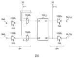
図6は、オーディオ信号処理回路200を示すブロック図である。このオーディオ信号処理回路200は、図1のDSP4のデジタル信号処理部20に相当するブロックと、FIRブロック202を備える。FIRブロック202は、上述のオーディオ信号処理回路100を備える。
FIG. 6 is a block diagram showing the audio
図6に示すように、単一のモジュール200の内部に、デジタル信号処理部20とFIRブロック202を混載する場合に、FIRブロック202には、デジタル信号処理部20からのオーディオ信号を受ける機能と、フィルタ処理後のオーディオ信号をデジタル信号処理部20に戻す機能と、が必要となる。
As shown in FIG. 6, when the digital
図7は、FIRブロック202の一部の構成例を示す図である。第1入力マルチプレクサ104Aには、デジタル信号処理部20からのオーディオ信号S11が入力される。FIRフィルタ106_iがデジタル信号処理部20からのオーディオ信号を処理対象とする場合、入力マルチプレクサ104は、信号S11を選択する。このとき、第2入力マルチプレクサ104Biはゼロを選択する。また第1レシーバ102Ai、第2レシーバ102Biはいずれもディセーブルである。これを第4状態φ4という。
FIG. 7 is a diagram illustrating a configuration example of a part of the
またFIRフィルタ106_iの出力に関して、FIRフィルタ106_iが最終段であり、フィルタ処理後のオーディオ信号S12をデジタル信号処理部20に戻す際には、第1トランスミッタ108Ai、第2トランスミッタ108Biはいずれもディセーブルとなる。これを第4状態φwという。
Regarding the output of the FIR filter 106_i, the FIR filter 106_i is the final stage, and when the audio signal S12 after the filter processing is returned to the digital
図6のオーディオ信号処理回路200を複数の個、組み合わせることにより、チャンネル数や要求される音質に応じて、FIRフィルタの規模を自由に設計することができる。
By combining a plurality of audio
続いてオーディオ信号処理回路100を利用したオーディオシステム1の用途を説明する。図8は、車載用オーディオ装置500の構成を示すブロック図である。車載用オーディオ装置500は、5.1チャンネル(フロント右FR、リア右RR、フロント左FL、リア左RL、センターC、サブウーファSW)で構成される。
Next, the application of the
デジタル音源2dは、CDプレイヤやDVDプレイヤなどであり、アナログ音源3は、チューナやモバイルオーディオプレイヤなどである。
The
デジタル音源2dからのデジタルオーディオ信号は、DSP4のデジタル入力端子に入力される。またチューナからのステレオ(Lch、Rch)のアナログオーディオ信号は、TUNERチャンネルに入力され、その他のモバイルオーディオプレイヤなどからのステレオアナログオーディオ信号はAUXチャンネルに入力される。
The digital audio signal from the
入力セレクタ502およびアンプ504は、RチャンネルとLチャンネルそれぞれに設けられる。入力セレクタ502は、入力チャンネル(Tuner/AUX)を選択し、選択されたチャンネルのシングルエンド形式のアナログオーディオ信号を差動信号に変換する。選択されたチャンネルに差動形式のオーディオ信号が入力される場合、差動変換処理はスキップされる。
The
アナログ/デジタル変換器505Rは、Rチャンネルの差動形式の入力オーディオ信号をデジタルオーディオ信号D1Rに変換し、アナログ/デジタル変換器505Lは、Lチャンネルの差動形式の入力オーディオ信号をデジタルオーディオ信号D1Lに変換する。図7において、アナログ/デジタル変換器505L、505Rの出力信号D1R、D1Lのペア、あるいはデジタル音源2dの出力が、図2におけるデジタルオーディオ信号S1に相当する。
The analog / digital converter 505R converts the R-channel differential input audio signal into the digital audio signal D1R, and the analog /
DSP4は、デジタルボリウム回路、5バンドイコライザ、ラウドネス回路、クロスオーバフィルタ、バスブースト回路を備え、デジタル音源2dの出力信号あるいはアナログ/デジタル変換器505L、505Rの出力信号D1R、D1Lのペアに対して、所定の信号処理を施す。このDSP4は、図5のオーディオ信号処理回路300、あるいは図6のオーディオ信号処理回路200に相当する。
The
DPS4は、LチャンネルおよびRチャンネルのオーディオ信号を、センドポートSENDから出力する。DSP4には、複数のFIRチップ5_1〜5_3が接続される。FIRチップ5は、図2のオーディオ信号処理回路100、図5のFIRチップ302、あるいは図6のオーディオ信号処理回路200のいずれかである。FIRチップ5の個数は、要求される音質に応じて変更可能である。たとえば3個のFIRチップ5は、図4(b)の態様で接続されてもよい。
The
フィルタ処理後のオーディオ信号は、DSP4のリターンポートRTNに戻される。DSP4は、残りの信号処理を施し、Lチャンネル、RチャンネルおよびMチャンネルのオーディオ信号を出力する。D/Aコンバータ507、アンプ506、ポストフィルタ508はL,R,Mチャンネルごとに設けられる。
The filtered audio signal is returned to the return port RTN of the
D/Aコンバータ507はチャンネルごとに設けられ、対応するチャンネルのオーディオ信号をアナログオーディオ信号に変換する。アンプ506は対応するチャンネルのオーディオ信号を増幅する。
The D / A converter 507 is provided for each channel, and converts the audio signal of the corresponding channel into an analog audio signal. The
3チャンネルのオーディオ信号は、ポストフィルタ508、フェーダボリウム510を経て、オーディオ信号は、スピーカごとの5チャンネルに分割される。パワーアンプ8は、オーディオ信号を増幅し、スピーカ9を駆動する。
The three-channel audio signal passes through a
実施の形態に係るオーディオ信号処理回路100は、このような車載用オーディオ装置500に好適に利用できる。
The audio
オーディオ信号処理回路100は車載用オーディオ装置のみでなく、家庭用のホームオーディオシステムのオーディオコンポーネント装置に利用することもできる。あるいは、オーディオ信号処理回路100は、テレビ、デスクトップPC、ノートPC、タブレットPC、携帯電話端末、デジタルカメラ、ポータブルオーディオプレイヤなどの電子機器に搭載することもできる。
The audio
図9(a)〜(c)は、電子機器あるいはオーディオコンポーネント装置の外観図である。図9(a)は電子機器の一例であるディスプレイ装置600である。ディスプレイ装置600は、筐体602、スピーカ9を備える。オーディオ信号処理回路100は、図示しないDSP4、パワーアンプ8等とともに筐体に内蔵される。
9A to 9C are external views of electronic devices or audio component devices. FIG. 9A illustrates a
図9(b)はオーディオコンポ700である。オーディオコンポ700は、筐体702、スピーカ9を備える。オーディオ信号処理回路100は図示しないDSP4、パワーアンプ8等とともに筐体に内蔵される。
FIG. 9B shows an
図9(c)は電子機器の一例である小型情報端末800である。小型情報端末800は、スマートホン、携帯電話、PHS(Personal Handy-phone System)、PDA(Personal Digital Assistant)、タブレットPC(Personal Computer)、オーディオプレイヤなどである。小型情報端末800は、筐体802、スピーカ9、ディスプレイ804を備える。オーディオ信号処理回路100は、図示しないDSP4、パワーアンプ8などとともに筐体に内蔵される。
FIG. 9C illustrates a
以上、本発明について、実施の形態をもとに説明した。この実施の形態は例示であり、それらの各構成要素や各処理プロセスの組み合わせにいろいろな変形例が可能なこと、またそうした変形例も本発明の範囲にあることは当業者に理解されるところである。以下、こうした変形例について説明する。 The present invention has been described based on the embodiments. This embodiment is an exemplification, and it will be understood by those skilled in the art that various modifications can be made to combinations of the respective constituent elements and processing processes, and such modifications are within the scope of the present invention. is there. Hereinafter, such modifications will be described.
(第1変形例)
実施の形態では、第2入力マルチプレクサ104Bが3入力の場合を説明したが、その他の構成としてもよい。たとえば第2レシーバ102Bをそのディセーブル状態においてゼロを出力するよう構成し、第3状態φ3において第2入力マルチプレクサ104Bが第2レシーバ102Bの出力を選択するよう構成してもよい。
(First modification)
Although the case where the second input multiplexer 104B has three inputs has been described in the embodiment, other configurations may be employed. For example, the second receiver 102B may be configured to output zero in its disabled state, and the second input multiplexer 104B may be configured to select the output of the second receiver 102B in the third state φ3.
(第2変形例)
また、複数の状態φ1〜φ3を切りかえる手段としては、第1入力マルチプレクサ104A、第2入力マルチプレクサ104Bを用いることに変えて、あるいはそれに加えて、FIRフィルタ106の出力側にデマルチプレクサを配置して実現してもよい。あるいは、マルチプレクサは、加算器で代用してもよい。すなわち信号Aと信号Bの一方を選択するマルチプレクサを信号AとBを加算する加算器で構成し、選択しない一方がゼロとなるように制御してもよい。
(Second modification)
As a means for switching between the plurality of states φ1 to φ3, a demultiplexer is arranged on the output side of the
(第3変形例)
実施の形態では、コントローラ120によってオーディオ信号処理回路100の内部の状態を制御したが本発明はそれには限定されない。マルチプレクサやレシーバの状態は、ヒューズを用いたメモリや、レーザトリミングを利用して不可逆的に設定してもよい。
(Third Modification)
In the embodiment, the
実施の形態にもとづき、具体的な語句を用いて本発明を説明したが、実施の形態は、本発明の原理、応用を示しているにすぎず、実施の形態には、請求の範囲に規定された本発明の思想を逸脱しない範囲において、多くの変形例や配置の変更が認められる。 Although the present invention has been described using specific terms based on the embodiments, the embodiments only illustrate the principles and applications of the present invention, and the embodiments are defined in the claims. Many variations and modifications of the arrangement are permitted without departing from the spirit of the present invention.
1…オーディオシステム、2d…デジタル音源、2a…アナログ音源、4…DSP、5…FIRチップ、8…パワーアンプ、9…電気音響変換素子、10…A/Dコンバータ、12…マルチプレクサ、20…デジタル信号処理部、100…オーディオ信号処理回路、IN…入力ポート、OUT…出力ポート、102…レシーバ、102A…第1レシーバ、102B…第2レシーバ、104…入力マルチプレクサ、104A…第1入力マルチプレクサ、104B…第2入力マルチプレクサ、106…FIRフィルタ、108…トランスミッタ、108A…第1トランスミッタ、108B…第2トランスミッタ、120…コントローラ、200…オーディオ信号処理回路、202…FIRブロック、300…オーディオ信号処理回路、302…FIRチップ。
DESCRIPTION OF
Claims (14)
前記複数N個のFIRフィルタと対応するN個の第1入力ポートと、
前記複数N個のFIRフィルタと対応するN個の第2入力ポートと、
前記複数N個のFIRフィルタと対応するN個の第1出力ポートと、
前記複数N個のFIRフィルタと対応するN個の第2出力ポートと、
を備え、ひとつの半導体基板に集積化され、
各FIRフィルタは、
第1入力端子と、
第2入力端子と、
第1出力端子と、
第2出力端子と、
前記第1入力端子と前記第1出力端子の間に直列接続された複数m個(mは2以上の整数)の遅延素子と、
前記m個の遅延素子に設けられた複数のタップのデータに所定の係数を乗算する複数の乗算器と、
前記第2入力端子に入力されたデータおよび前記複数の乗算器の出力データの加算結果である積和データを前記第2出力端子から出力する加算回路と、
を含み、
i番目(2≦i≦N)のFIRフィルタに関して、
(i)その前記第1入力端子に、(i−1)番目のFIRフィルタの前記第1出力端子のデータが入力され、かつその前記第2入力端子に、(i−1)番目のFIRフィルタの前記第2出力端子のデータが入力される状態と、
(ii)その前記第1入力端子に、i番目の前記第1入力ポートのデータが入力され、かつその前記第2入力端子に、i番目の前記第2入力ポートのデータが入力された状態と、
(iii)その前記第1入力端子に、i番目の前記第1入力ポートのデータが入力され、かつその前記第2入力端子にゼロが入力される状態と、
が切りかえ可能に構成されることを特徴とするオーディオ信号処理回路。 A plurality of N (N is an integer of 2 or more) FIR (Finite Impulse Response) filters;
N first input ports corresponding to the plurality of N FIR filters;
N second input ports corresponding to the plurality of N FIR filters;
N first output ports corresponding to the plurality of N FIR filters;
N second output ports corresponding to the plurality of N FIR filters;
Integrated on a single semiconductor substrate,
Each FIR filter is
A first input terminal;
A second input terminal;
A first output terminal;
A second output terminal;
A plurality of m (m is an integer of 2 or more) delay elements connected in series between the first input terminal and the first output terminal;
A plurality of multipliers for multiplying data of a plurality of taps provided in the m delay elements by a predetermined coefficient;
An adder circuit that outputs sum-of-product data that is a result of adding the data input to the second input terminal and the output data of the plurality of multipliers from the second output terminal;
Including
For the i th (2 ≦ i ≦ N) FIR filter,
(I) The data of the first output terminal of the (i-1) th FIR filter is input to the first input terminal, and the (i-1) th FIR filter is input to the second input terminal. A state in which data of the second output terminal is input;
(Ii) a state in which data of the i-th first input port is input to the first input terminal, and data of the i-th second input port is input to the second input terminal; ,
(Iii) a state in which data of the i-th first input port is input to the first input terminal and zero is input to the second input terminal;
An audio signal processing circuit characterized by being configured to be switchable.
2〜N番目のFIRフィルタに対応する(N−1)個の第2入力マルチプレクサと、
をさらに備え、
i(2≦i≦N)番目の第1入力マルチプレクサは、(i−1)番目のFIRフィルタの前記第1出力端子のデータとi番目の第1入力ポートのデータを受け、一方を選択して、i番目のFIRフィルタの第1入力端子に出力し、
i(2≦i≦N)番目の第2入力マルチプレクサは、(i−1)番目のFIRフィルタの前記第2出力端子のデータとi番目の第2入力ポートのデータを受け、それらの一方またはゼロを、i番目のFIRフィルタの第2入力端子に出力することを特徴とする請求項1に記載のオーディオ信号処理回路。 (N-1) first input multiplexers corresponding to the 2nd to Nth FIR filters;
(N-1) second input multiplexers corresponding to the 2nd to Nth FIR filters;
Further comprising
The i (2 ≦ i ≦ N) th first input multiplexer receives the data of the first output terminal of the (i−1) th FIR filter and the data of the ith first input port, and selects one of them. Output to the first input terminal of the i-th FIR filter,
The i (2 ≦ i ≦ N) second input multiplexer receives the data of the second output terminal of the (i−1) th FIR filter and the data of the i th second input port, and either one of them or The audio signal processing circuit according to claim 1, wherein zero is output to a second input terminal of the i-th FIR filter.
前記1番目の第1入力マルチプレクサは、前記オーディオ信号処理回路内の別の第1回路ブロックからの入力データと、1番目の第1入力ポートのデータと、を受け、一方を選択して1番目のFIRフィルタの前記第1入力端子に出力することを特徴とする請求項1から3のいずれかに記載のオーディオ信号処理回路。 A first first input multiplexer corresponding to the first FIR filter;
The first first input multiplexer receives input data from another first circuit block in the audio signal processing circuit and data of the first first input port, selects one and selects the first The audio signal processing circuit according to claim 1, wherein the audio signal processing circuit outputs the signal to the first input terminal of the FIR filter.
前記N個の第2入力ポートに対応し、それぞれが対応する第2入力ポートのデータを受けるN個の第2レシーバと、
をさらに備えることを特徴とする請求項1から5のいずれかに記載のオーディオ信号処理回路。 N first receivers corresponding to the N first input ports, each receiving data of the corresponding first input port;
N second receivers corresponding to the N second input ports, each receiving data of the corresponding second input port;
The audio signal processing circuit according to claim 1, further comprising:
前記N個のFIRフィルタに対応し、それぞれが対応するFIRフィルタの第2出力端子のデータを受け、対応する第2出力ポートに出力する、N個の第2トランスミッタと、
をさらに備えることを特徴とする請求項1から8のいずれかに記載のオーディオ信号処理回路。 N first transmitters corresponding to the N FIR filters, each receiving data at a first output terminal of the corresponding FIR filter and outputting the data to a corresponding first output port;
N second transmitters corresponding to the N FIR filters, each receiving data at the second output terminal of the corresponding FIR filter and outputting the data to the corresponding second output port;
The audio signal processing circuit according to claim 1, further comprising:
Priority Applications (2)
| Application Number | Priority Date | Filing Date | Title |
|---|---|---|---|
| JP2014248809A JP6474246B2 (en) | 2014-12-09 | 2014-12-09 | Audio signal processing circuit, in-vehicle audio device, audio component device, electronic equipment |
| EP15198392.1A EP3032743B1 (en) | 2014-12-09 | 2015-12-08 | Audio signal processing circuit, car audio apparatus, audio component apparatus, and electronic device |
Applications Claiming Priority (1)
| Application Number | Priority Date | Filing Date | Title |
|---|---|---|---|
| JP2014248809A JP6474246B2 (en) | 2014-12-09 | 2014-12-09 | Audio signal processing circuit, in-vehicle audio device, audio component device, electronic equipment |
Publications (2)
| Publication Number | Publication Date |
|---|---|
| JP2016111593A JP2016111593A (en) | 2016-06-20 |
| JP6474246B2 true JP6474246B2 (en) | 2019-02-27 |
Family
ID=54843698
Family Applications (1)
| Application Number | Title | Priority Date | Filing Date |
|---|---|---|---|
| JP2014248809A Active JP6474246B2 (en) | 2014-12-09 | 2014-12-09 | Audio signal processing circuit, in-vehicle audio device, audio component device, electronic equipment |
Country Status (2)
| Country | Link |
|---|---|
| EP (1) | EP3032743B1 (en) |
| JP (1) | JP6474246B2 (en) |
Family Cites Families (9)
| Publication number | Priority date | Publication date | Assignee | Title |
|---|---|---|---|---|
| JPH01126819A (en) * | 1987-11-12 | 1989-05-18 | Matsushita Electric Ind Co Ltd | digital signal processing equipment |
| JP2639543B2 (en) * | 1987-12-02 | 1997-08-13 | 日本ビクター株式会社 | Digital filter device |
| JP2884571B2 (en) * | 1988-04-12 | 1999-04-19 | ソニー株式会社 | Digital signal processing circuit |
| JPH0423609A (en) * | 1990-05-18 | 1992-01-28 | Nec Corp | Fir digital filter |
| JPH0437212A (en) | 1990-05-31 | 1992-02-07 | Victor Co Of Japan Ltd | Fir digital filtering device |
| US5157395A (en) * | 1991-03-04 | 1992-10-20 | Crystal Semiconductor Corporation | Variable decimation architecture for a delta-sigma analog-to-digital converter |
| JPH07176989A (en) * | 1993-12-20 | 1995-07-14 | Yamaha Corp | Digital signal processing circuit |
| JP4222808B2 (en) | 2002-09-30 | 2009-02-12 | 富士通テン株式会社 | DSP equipment |
| JP2005020554A (en) * | 2003-06-27 | 2005-01-20 | Neuro Solution Corp | Digital filter |
-
2014
- 2014-12-09 JP JP2014248809A patent/JP6474246B2/en active Active
-
2015
- 2015-12-08 EP EP15198392.1A patent/EP3032743B1/en active Active
Also Published As
| Publication number | Publication date |
|---|---|
| EP3032743A1 (en) | 2016-06-15 |
| EP3032743B1 (en) | 2017-06-28 |
| JP2016111593A (en) | 2016-06-20 |
Similar Documents
| Publication | Publication Date | Title |
|---|---|---|
| CN103888103B (en) | system and method for digital signal processing | |
| CN102804810B (en) | spectrum management system | |
| TWI536370B (en) | System and method for digital signal processing | |
| US8094835B2 (en) | Signal processing apparatus | |
| US9143104B2 (en) | Audio signal processing circuit, car audio apparatus using the same, audio component apparatus, electronic device and output audio signal generating method | |
| Self | The Design of Active Crossovers | |
| US8139789B2 (en) | Signal amplifier circuit | |
| JP6737597B2 (en) | Audio digital signal processing device and vehicle-mounted audio device and electronic equipment using the same | |
| US10938363B2 (en) | Audio circuit | |
| CN113810829B (en) | Method and device for processing audio signal | |
| JP6474246B2 (en) | Audio signal processing circuit, in-vehicle audio device, audio component device, electronic equipment | |
| JP6018491B2 (en) | D / A conversion circuit, zero cross point detection method, in-vehicle audio apparatus, audio component apparatus, and electronic apparatus using the same | |
| CN101682301B (en) | Multimode Audio Amplifier | |
| JP4840641B2 (en) | Audio signal delay time difference automatic correction device | |
| CN108469948A (en) | Terminal and audio-frequency inputting method | |
| TW201426739A (en) | System and method for digital signal processing | |
| JP5993733B2 (en) | Mixing circuit, in-vehicle audio device, audio component device, and electronic device using the same | |
| JP2001128299A (en) | Signal processing device, headphone device and speaker device using the same | |
| US20180197563A1 (en) | Audio signal processing circuit, in-vehicle audio system, audio component device and electronic apparatus including the same, and method of processing audio signal | |
| CN119673195A (en) | A vehicle-mounted sadsp system | |
| GB2447634A (en) | Sound output device with earphone mode and speaker mode |
Legal Events
| Date | Code | Title | Description |
|---|---|---|---|
| A621 | Written request for application examination |
Free format text: JAPANESE INTERMEDIATE CODE: A621 Effective date: 20171110 |
|
| TRDD | Decision of grant or rejection written | ||
| A01 | Written decision to grant a patent or to grant a registration (utility model) |
Free format text: JAPANESE INTERMEDIATE CODE: A01 Effective date: 20190108 |
|
| A61 | First payment of annual fees (during grant procedure) |
Free format text: JAPANESE INTERMEDIATE CODE: A61 Effective date: 20190129 |
|
| R150 | Certificate of patent or registration of utility model |
Ref document number: 6474246 Country of ref document: JP Free format text: JAPANESE INTERMEDIATE CODE: R150 |
|
| R250 | Receipt of annual fees |
Free format text: JAPANESE INTERMEDIATE CODE: R250 |
|
| R250 | Receipt of annual fees |
Free format text: JAPANESE INTERMEDIATE CODE: R250 |
|
| R250 | Receipt of annual fees |
Free format text: JAPANESE INTERMEDIATE CODE: R250 |
|
| R250 | Receipt of annual fees |
Free format text: JAPANESE INTERMEDIATE CODE: R250 |
|
| R250 | Receipt of annual fees |
Free format text: JAPANESE INTERMEDIATE CODE: R250 |