JP6478884B2 - 半導体装置 - Google Patents
半導体装置 Download PDFInfo
- Publication number
- JP6478884B2 JP6478884B2 JP2015179039A JP2015179039A JP6478884B2 JP 6478884 B2 JP6478884 B2 JP 6478884B2 JP 2015179039 A JP2015179039 A JP 2015179039A JP 2015179039 A JP2015179039 A JP 2015179039A JP 6478884 B2 JP6478884 B2 JP 6478884B2
- Authority
- JP
- Japan
- Prior art keywords
- sic
- region
- type
- metal layer
- semiconductor device
- Prior art date
- Legal status (The legal status is an assumption and is not a legal conclusion. Google has not performed a legal analysis and makes no representation as to the accuracy of the status listed.)
- Active
Links
Images




Classifications
-
- H—ELECTRICITY
- H10—SEMICONDUCTOR DEVICES; ELECTRIC SOLID-STATE DEVICES NOT OTHERWISE PROVIDED FOR
- H10D—INORGANIC ELECTRIC SEMICONDUCTOR DEVICES
- H10D30/00—Field-effect transistors [FET]
- H10D30/60—Insulated-gate field-effect transistors [IGFET]
- H10D30/64—Double-diffused metal-oxide semiconductor [DMOS] FETs
- H10D30/66—Vertical DMOS [VDMOS] FETs
- H10D30/668—Vertical DMOS [VDMOS] FETs having trench gate electrodes, e.g. UMOS transistors
-
- H—ELECTRICITY
- H10—SEMICONDUCTOR DEVICES; ELECTRIC SOLID-STATE DEVICES NOT OTHERWISE PROVIDED FOR
- H10D—INORGANIC ELECTRIC SEMICONDUCTOR DEVICES
- H10D30/00—Field-effect transistors [FET]
- H10D30/60—Insulated-gate field-effect transistors [IGFET]
- H10D30/63—Vertical IGFETs
-
- H—ELECTRICITY
- H10—SEMICONDUCTOR DEVICES; ELECTRIC SOLID-STATE DEVICES NOT OTHERWISE PROVIDED FOR
- H10D—INORGANIC ELECTRIC SEMICONDUCTOR DEVICES
- H10D62/00—Semiconductor bodies, or regions thereof, of devices having potential barriers
- H10D62/10—Shapes, relative sizes or dispositions of the regions of the semiconductor bodies; Shapes of the semiconductor bodies
- H10D62/102—Constructional design considerations for preventing surface leakage or controlling electric field concentration
- H10D62/103—Constructional design considerations for preventing surface leakage or controlling electric field concentration for increasing or controlling the breakdown voltage of reverse-biased devices
- H10D62/105—Constructional design considerations for preventing surface leakage or controlling electric field concentration for increasing or controlling the breakdown voltage of reverse-biased devices by having particular doping profiles, shapes or arrangements of PN junctions; by having supplementary regions, e.g. junction termination extension [JTE]
- H10D62/106—Constructional design considerations for preventing surface leakage or controlling electric field concentration for increasing or controlling the breakdown voltage of reverse-biased devices by having particular doping profiles, shapes or arrangements of PN junctions; by having supplementary regions, e.g. junction termination extension [JTE] having supplementary regions doped oppositely to or in rectifying contact with regions of the semiconductor bodies, e.g. guard rings with PN or Schottky junctions
- H10D62/107—Buried supplementary regions, e.g. buried guard rings
-
- H—ELECTRICITY
- H10—SEMICONDUCTOR DEVICES; ELECTRIC SOLID-STATE DEVICES NOT OTHERWISE PROVIDED FOR
- H10D—INORGANIC ELECTRIC SEMICONDUCTOR DEVICES
- H10D62/00—Semiconductor bodies, or regions thereof, of devices having potential barriers
- H10D62/10—Shapes, relative sizes or dispositions of the regions of the semiconductor bodies; Shapes of the semiconductor bodies
- H10D62/17—Semiconductor regions connected to electrodes not carrying current to be rectified, amplified or switched, e.g. channel regions
- H10D62/393—Body regions of DMOS transistors or IGBTs
-
- H—ELECTRICITY
- H10—SEMICONDUCTOR DEVICES; ELECTRIC SOLID-STATE DEVICES NOT OTHERWISE PROVIDED FOR
- H10D—INORGANIC ELECTRIC SEMICONDUCTOR DEVICES
- H10D62/00—Semiconductor bodies, or regions thereof, of devices having potential barriers
- H10D62/80—Semiconductor bodies, or regions thereof, of devices having potential barriers characterised by the materials
- H10D62/83—Semiconductor bodies, or regions thereof, of devices having potential barriers characterised by the materials being Group IV materials, e.g. B-doped Si or undoped Ge
- H10D62/832—Semiconductor bodies, or regions thereof, of devices having potential barriers characterised by the materials being Group IV materials, e.g. B-doped Si or undoped Ge being Group IV materials comprising two or more elements, e.g. SiGe
- H10D62/8325—Silicon carbide
-
- H—ELECTRICITY
- H10—SEMICONDUCTOR DEVICES; ELECTRIC SOLID-STATE DEVICES NOT OTHERWISE PROVIDED FOR
- H10D—INORGANIC ELECTRIC SEMICONDUCTOR DEVICES
- H10D64/00—Electrodes of devices having potential barriers
- H10D64/01—Manufacture or treatment
- H10D64/013—Manufacture or treatment of electrodes having a conductor capacitively coupled to a semiconductor by an insulator
- H10D64/01366—Manufacture or treatment of electrodes having a conductor capacitively coupled to a semiconductor by an insulator the semiconductor being silicon carbide
-
- H—ELECTRICITY
- H10—SEMICONDUCTOR DEVICES; ELECTRIC SOLID-STATE DEVICES NOT OTHERWISE PROVIDED FOR
- H10D—INORGANIC ELECTRIC SEMICONDUCTOR DEVICES
- H10D64/00—Electrodes of devices having potential barriers
- H10D64/20—Electrodes characterised by their shapes, relative sizes or dispositions
- H10D64/23—Electrodes carrying the current to be rectified, amplified, oscillated or switched, e.g. sources, drains, anodes or cathodes
- H10D64/251—Source or drain electrodes for field-effect devices
- H10D64/252—Source or drain electrodes for field-effect devices for vertical or pseudo-vertical devices
- H10D64/2527—Source or drain electrodes for field-effect devices for vertical or pseudo-vertical devices for vertical devices wherein the source or drain electrodes are recessed in semiconductor bodies
-
- H—ELECTRICITY
- H10—SEMICONDUCTOR DEVICES; ELECTRIC SOLID-STATE DEVICES NOT OTHERWISE PROVIDED FOR
- H10D—INORGANIC ELECTRIC SEMICONDUCTOR DEVICES
- H10D64/00—Electrodes of devices having potential barriers
- H10D64/20—Electrodes characterised by their shapes, relative sizes or dispositions
- H10D64/27—Electrodes not carrying the current to be rectified, amplified, oscillated or switched, e.g. gates
- H10D64/311—Gate electrodes for field-effect devices
- H10D64/411—Gate electrodes for field-effect devices for FETs
- H10D64/511—Gate electrodes for field-effect devices for FETs for IGFETs
- H10D64/512—Disposition of the gate electrodes, e.g. buried gates
- H10D64/513—Disposition of the gate electrodes, e.g. buried gates within recesses in the substrate, e.g. trench gates, groove gates or buried gates
-
- H—ELECTRICITY
- H10—SEMICONDUCTOR DEVICES; ELECTRIC SOLID-STATE DEVICES NOT OTHERWISE PROVIDED FOR
- H10D—INORGANIC ELECTRIC SEMICONDUCTOR DEVICES
- H10D64/00—Electrodes of devices having potential barriers
- H10D64/60—Electrodes characterised by their materials
- H10D64/64—Electrodes comprising a Schottky barrier to a semiconductor
-
- H—ELECTRICITY
- H10—SEMICONDUCTOR DEVICES; ELECTRIC SOLID-STATE DEVICES NOT OTHERWISE PROVIDED FOR
- H10D—INORGANIC ELECTRIC SEMICONDUCTOR DEVICES
- H10D84/00—Integrated devices formed in or on semiconductor substrates that comprise only semiconducting layers, e.g. on Si wafers or on GaAs-on-Si wafers
- H10D84/101—Integrated devices comprising main components and built-in components, e.g. IGBT having built-in freewheel diode
- H10D84/141—VDMOS having built-in components
- H10D84/146—VDMOS having built-in components the built-in components being Schottky barrier diodes
-
- H—ELECTRICITY
- H10—SEMICONDUCTOR DEVICES; ELECTRIC SOLID-STATE DEVICES NOT OTHERWISE PROVIDED FOR
- H10P—GENERIC PROCESSES OR APPARATUS FOR THE MANUFACTURE OR TREATMENT OF DEVICES COVERED BY CLASS H10
- H10P32/00—Diffusion of dopants within, into or out of wafers, substrates or parts of devices
- H10P32/10—Diffusion of dopants within, into or out of semiconductor bodies or layers
- H10P32/17—Diffusion of dopants within, into or out of semiconductor bodies or layers characterised by the semiconductor material
- H10P32/171—Diffusion of dopants within, into or out of semiconductor bodies or layers characterised by the semiconductor material being group IV material
- H10P32/172—Diffusion of dopants within, into or out of semiconductor bodies or layers characterised by the semiconductor material being group IV material being crystalline silicon carbide
Landscapes
- Electrodes Of Semiconductors (AREA)
Description
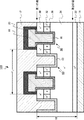
本実施形態の半導体装置は、第1の面と第2の面とを有するSiC層と、SiC層内に設けられたn型の第1のSiC領域と、第1のSiC領域と第1の面との間に設けられた複数のp型の第2のSiC領域と、第2のSiC領域と第1の面との間に設けられた複数のn型の第3のSiC領域と、複数のp型の第2のSiC領域の内の2つのp型の第2のSiC領域の間に設けられたゲート電極と、ゲート電極と、第1のSiC領域及び第2のSiC領域との間に設けられ、第1のSiC領域及び第2のSiC領域に接するゲート絶縁膜と、第1のSiC領域に接し、仕事関数が6.5eV以上の金属層と、金属層に電気的に接続された第1の電極と、第2の面に設けられた第2の電極と、を備え、ゲート絶縁膜と金属層との間に、第1のSiC領域の一部が挟まれる。
本実施形態の半導体装置は、ゲート電極の材料に、p型不純物を含む3C−SiCを適用する以外は、第1の実施形態と同様である。したがって、第1の実施形態と重複する内容については記述を省略する。
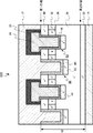
本実施形態の半導体装置は、金属層の第2の面側の端部と第1のSiC領域との間に、p型の第5のSiC領域を、更に備える点、ゲート絶縁膜の第2の面側の端部と第1のSiC領域との間に、p型の第6のSiC領域を、更に備える点以外は、第1の実施形態と同様である。言い換えれば、本実施形態の半導体装置は、第2のトレンチの底部と第1のSiC領域との間に、p型の第5のSiC領域を、更に備える点、第1のトレンチの底部と第1のSiC領域との間に、p型の第6のSiC領域を、更に備える点以外は、第1の実施形態と同様である。したがって、第1の実施形態と重複する内容については記述を省略する。
本実施形態の半導体装置は、ダブルショットキーダイオードを備える点以外は、第1の実施形態と同様である。したがって、第1の実施形態と重複する内容については記述を省略する。
本実施形態の半導体装置は、第2のトレンチが金属層のみで埋め込まれている点以外はは、第1の実施形態と同様である。したがって、第1の実施形態と重複する内容については記述を省略する。
本実施形態の半導体装置は、ゲート電極が第1の金属膜と第2の金属膜の積層構造である点で、第2の実施形態と異なる。したがって、第2の実施形態と重複する内容については記述を省略する。
本実施形態の半導体装置は、第2のトレンチ内にソース電極の一部が埋め込まれる以下は、第4の実施形態と同様である。
12 ソース電極(第1の電極)
14 ドレイン電極(第2の電極)
16 ゲート絶縁膜
18 ゲート電極
22 ドレイン領域
24 ドリフト領域(n型の第1のSiC領域)
26 ウェル領域(p型の第2のSiC領域)
30 ソース領域(n型の第3のSiC領域)
32 ウェルコンタクト領域(p型の第4のSiC領域)
40 金属層
42 アノード領域(p型の第5のSiC領域)
44 電界緩和領域(p型の第6のSiC領域)
50 第1のトレンチ
60 第2のトレンチ
100 MOSFET(半導体装置)
200 MOSFET(半導体装置)
300 MOSFET(半導体装置)
400 MOSFET(半導体装置)
500 MOSFET(半導体装置)
600 MOSFET(半導体装置)
Claims (20)
- 第1の面と第2の面とを有するSiC層と、
前記SiC層内に設けられたn型の第1のSiC領域と、
前記第1のSiC領域と前記第1の面との間に設けられた複数のp型の第2のSiC領域と、
前記第2のSiC領域と前記第1の面との間に設けられた複数のn型の第3のSiC領域と、
前記複数のp型の第2のSiC領域の内の2つのp型の第2のSiC領域の間に設けられたゲート電極と、
前記ゲート電極と、前記第1のSiC領域及び前記第2のSiC領域との間に設けられ、前記第1のSiC領域及び前記第2のSiC領域に接するゲート絶縁膜と、
前記第1のSiC領域に接し、仕事関数が6.5eV以上の金属層と、
前記金属層に電気的に接続された第1の電極と、
前記第2の面に設けられた第2の電極と、
を備え、
前記ゲート絶縁膜と前記金属層との間に、前記第1のSiC領域の一部が挟まれる半導体装置。 - 前記金属層は、p型不純物の濃度が1×1020cm−3以上のSiCを含む請求項1記載の半導体装置。
- 前記p型不純物は、アルミニウム(Al)、ガリウム(Ga)及びインジウム(In)から選ばれた少なくとも一つである請求項2記載の半導体装置。
- 前記SiCは、3C−SiCを含む請求項2記載の半導体装置。
- 前記金属層と前記第1のSiC領域との間の接合は、ショットキー接合である請求項1乃至請求項4いずれか一項記載の半導体装置。
- 前記金属層と前記第2のSiC領域との間に、前記第2のSiC領域よりもp型不純物濃度の高いp型の第4のSiC領域を更に備え、前記金属層が前記第4のSiC領域に接する請求項1乃至請求項5いずれか一項記載の半導体装置。
- 前記金属層の前記第2の面側の端部と前記第1のSiC領域との間に、p型の第5のSiC領域を、更に備える請求項1乃至請求項6いずれか一項記載の半導体装置。
- 前記金属層の前記第2の面側の端部の深さが、前記第ゲート絶縁膜前記第2の面側の端部よりも深い請求項1乃至請求項7いずれか一項記載の半導体装置。
- 前記ゲート電極は、アルミニウム(Al)、ガリウム(Ga)及びインジウム(In)から選ばれた少なくとも一つを含む3C−SiCを含む請求項1乃至請求項8いずれか一項記載の半導体装置。
- 前記ゲート電極は第1の金属膜と第2の金属膜とを備え、前記第1の金属膜が前記金属層と略同一の材料、且つ、略同一の膜厚である請求項1乃至請求項9いずれか一項記載の半導体装置。
- 第1の面と第2の面とを有し、前記第1の面に設けられた第1のトレンチ及び第2のトレンチを有するSiC層と、
前記SiC層内に設けられたn型の第1のSiC領域と、
前記第1のSiC領域と前記第1の面との間に設けられたp型の第2のSiC領域と、
前記第2のSiC領域と前記第1の面との間に設けられたn型の第3のSiC領域と、
前記第1のトレンチ内に設けられ、前記第1のSiC領域及び前記第2のSiC領域に接するゲート絶縁膜と、
前記第1のトレンチ内に設けられ、前記ゲート絶縁膜に接するゲート電極と、
前記第2のトレンチ内に設けられ、前記第1のSiC領域に接し、仕事関数が6.5eV以上の金属層と、
前記金属層に電気的に接続された第1の電極と、
前記第2の面に設けられた第2の電極と、
を備える半導体装置。 - 前記金属層は、p型不純物の濃度が1×1020cm−3以上のSiCを含む請求項11記載の半導体装置。
- 前記p型不純物は、アルミニウム(Al)、ガリウム(Ga)及びインジウム(In)から選ばれた少なくとも一つである請求項12記載の半導体装置。
- 前記SiCは、3C−SiCを含む請求項12記載の半導体装置。
- 前記金属層と前記第1のSiC領域との間の接合は、ショットキー接合である請求項11乃至請求項14いずれか一項記載の半導体装置。
- 前記金属層と前記第2のSiC領域との間に、前記第2のSiC領域よりもp型不純物濃度の高いp型の第4のSiC領域を更に備え、前記金属層が前記第4のSiC領域に接する請求項11乃至請求項15いずれか一項記載の半導体装置。
- 前記第2のトレンチの底部と前記第1のSiC領域との間に、p型の第5のSiC領域を、更に備える請求項11乃至請求項16いずれか一項記載の半導体装置。
- 前記第2のトレンチの深さが、前記第1のトレンチの深さよりも深い請求項11乃至請求項17いずれか一項記載の半導体装置。
- 前記ゲート電極は、アルミニウム(Al)、ガリウム(Ga)及びインジウム(In)から選ばれた少なくとも一つを含む3C−SiCを含む請求項11乃至請求項18いずれか一項記載の半導体装置。
- 前記ゲート電極は第1の金属膜と第2の金属膜とを備え、前記第1の金属膜が前記金属層と略同一の材料、且つ、略同一の膜厚である請求項11乃至請求項19いずれか一項記載の半導体装置。
Priority Applications (2)
| Application Number | Priority Date | Filing Date | Title |
|---|---|---|---|
| JP2015179039A JP6478884B2 (ja) | 2015-09-11 | 2015-09-11 | 半導体装置 |
| US15/252,466 US10229994B2 (en) | 2015-09-11 | 2016-08-31 | Semiconductor device |
Applications Claiming Priority (1)
| Application Number | Priority Date | Filing Date | Title |
|---|---|---|---|
| JP2015179039A JP6478884B2 (ja) | 2015-09-11 | 2015-09-11 | 半導体装置 |
Publications (2)
| Publication Number | Publication Date |
|---|---|
| JP2017055005A JP2017055005A (ja) | 2017-03-16 |
| JP6478884B2 true JP6478884B2 (ja) | 2019-03-06 |
Family
ID=58238989
Family Applications (1)
| Application Number | Title | Priority Date | Filing Date |
|---|---|---|---|
| JP2015179039A Active JP6478884B2 (ja) | 2015-09-11 | 2015-09-11 | 半導体装置 |
Country Status (2)
| Country | Link |
|---|---|
| US (1) | US10229994B2 (ja) |
| JP (1) | JP6478884B2 (ja) |
Families Citing this family (32)
| Publication number | Priority date | Publication date | Assignee | Title |
|---|---|---|---|---|
| JP6523885B2 (ja) | 2015-09-11 | 2019-06-05 | 株式会社東芝 | 半導体装置 |
| JP6526528B2 (ja) | 2015-09-11 | 2019-06-05 | 株式会社東芝 | 半導体装置 |
| JP6667893B2 (ja) * | 2015-10-20 | 2020-03-18 | 富士電機株式会社 | 半導体装置および半導体装置の製造方法 |
| JP6658406B2 (ja) * | 2016-08-31 | 2020-03-04 | 株式会社デンソー | 炭化珪素半導体装置の製造方法 |
| DE212018000102U1 (de) | 2017-05-17 | 2019-08-05 | Rohm Co., Ltd. | Halbleitervorrichtung |
| JP7201336B2 (ja) | 2017-05-17 | 2023-01-10 | ローム株式会社 | 半導体装置 |
| JP7081087B2 (ja) * | 2017-06-02 | 2022-06-07 | 富士電機株式会社 | 絶縁ゲート型半導体装置及びその製造方法 |
| JP6922535B2 (ja) * | 2017-08-04 | 2021-08-18 | 富士電機株式会社 | 半導体装置および半導体装置の製造方法 |
| JP6776205B2 (ja) * | 2017-09-20 | 2020-10-28 | 株式会社東芝 | 半導体装置の製造方法 |
| CN111357119B (zh) * | 2017-11-15 | 2023-11-24 | 株式会社Flosfia | 半导体装置 |
| DE102017128633B4 (de) * | 2017-12-01 | 2024-09-19 | Infineon Technologies Ag | Siliziumcarbid-halbleiterbauelement mit grabengatestrukturen und abschirmgebieten |
| JP7196403B2 (ja) | 2018-03-09 | 2022-12-27 | 富士電機株式会社 | 半導体装置 |
| DE102018106967B3 (de) | 2018-03-23 | 2019-05-23 | Infineon Technologies Ag | SILIZIUMCARBID HALBLEITERBAUELEMENT und Halbleiterdiode |
| JP7155641B2 (ja) * | 2018-06-14 | 2022-10-19 | 富士電機株式会社 | 半導体装置 |
| DE102018120734B4 (de) | 2018-08-24 | 2025-01-30 | Infineon Technologies Ag | Halbleitervorrichtung, die ein übergangsmaterial in einem graben enthält, und herstellungsverfahren |
| CN109148566B (zh) * | 2018-08-28 | 2020-11-13 | 电子科技大学 | 碳化硅mosfet器件及其制造方法 |
| JP7243094B2 (ja) * | 2018-09-11 | 2023-03-22 | 富士電機株式会社 | 半導体装置 |
| CN111384171B (zh) * | 2018-12-28 | 2021-07-23 | 中国科学院苏州纳米技术与纳米仿生研究所 | 高沟道迁移率垂直型umosfet器件及其制备方法 |
| US11411084B2 (en) * | 2020-07-09 | 2022-08-09 | Kabushiki Kaisha Toshiba | Semiconductor device, inverter circuit, drive device, vehicle, and elevator |
| JP7458257B2 (ja) * | 2020-07-09 | 2024-03-29 | 株式会社東芝 | 半導体装置、インバータ回路、駆動装置、車両、及び、昇降機 |
| TWI729952B (zh) * | 2020-10-22 | 2021-06-01 | 大陸商上海瀚薪科技有限公司 | 一種碳化矽半導體元件 |
| TWI745251B (zh) * | 2020-10-22 | 2021-11-01 | 大陸商上海瀚薪科技有限公司 | 一種碳化矽半導體元件 |
| DE102020215721A1 (de) * | 2020-12-11 | 2022-06-15 | Robert Bosch Gesellschaft mit beschränkter Haftung | Vertikaler feldeffekttransistor und verfahren zum herstellen desselben |
| JP7475265B2 (ja) * | 2020-12-14 | 2024-04-26 | 三菱電機株式会社 | 半導体装置及び半導体装置の製造方法 |
| DE102021104532B4 (de) * | 2021-02-25 | 2025-06-18 | Infineon Technologies Ag | Mesa-Kontakt für MOS-gesteuerte Leistungshalbleitervorrichtung undVerfahren zum Herstellen einer Leistungshalbleitervorrichtung |
| DE102022100072A1 (de) | 2022-01-03 | 2023-07-06 | Infineon Technologies Ag | Verfahren zum herstellen einer metallsilicidschicht oberhalb eines siliciumcarbidsubstrats und halbleitervorrichtung, die eine metallsilicidschicht umfasst |
| JP7559881B2 (ja) * | 2022-05-12 | 2024-10-02 | 富士電機株式会社 | 絶縁ゲート型半導体装置 |
| CN115498063A (zh) * | 2022-07-25 | 2022-12-20 | 核芯光电科技(山东)有限公司 | 一种基于栅极结构的Si-PIN探测装置及其制造方法 |
| JP7824851B2 (ja) | 2022-09-21 | 2026-03-05 | 株式会社東芝 | 半導体装置およびその製造方法 |
| CN115763524B (zh) * | 2022-11-22 | 2025-10-17 | 中国科学院苏州纳米技术与纳米仿生研究所 | 垂直增强型β-Ga2O3 UMOSFET器件及其制备方法 |
| JP7851878B2 (ja) * | 2023-03-14 | 2026-04-27 | 株式会社東芝 | 半導体装置 |
| CN117174763B (zh) * | 2023-11-03 | 2024-03-01 | 山东大学 | 碳化硅混合3C-SiC接触PN结肖特基二极管及制备方法 |
Family Cites Families (17)
| Publication number | Priority date | Publication date | Assignee | Title |
|---|---|---|---|---|
| JP3361061B2 (ja) * | 1998-09-17 | 2003-01-07 | 株式会社東芝 | 半導体装置 |
| US20050012143A1 (en) * | 2003-06-24 | 2005-01-20 | Hideaki Tanaka | Semiconductor device and method of manufacturing the same |
| JP5721308B2 (ja) * | 2008-03-26 | 2015-05-20 | ローム株式会社 | 半導体装置 |
| US7816732B2 (en) * | 2008-06-23 | 2010-10-19 | Force Mos Technology Co., Ltd. | Integrated trench MOSFET and Schottky rectifier with trench contact structure |
| US8188484B2 (en) | 2008-12-25 | 2012-05-29 | Rohm Co., Ltd. | Semiconductor device |
| US8188538B2 (en) * | 2008-12-25 | 2012-05-29 | Rohm Co., Ltd. | Semiconductor device and method of manufacturing semiconductor device |
| JP5721351B2 (ja) * | 2009-07-21 | 2015-05-20 | ローム株式会社 | 半導体装置 |
| JP5439215B2 (ja) | 2010-02-10 | 2014-03-12 | 株式会社東芝 | 半導体装置および半導体装置の製造方法 |
| JP5498431B2 (ja) * | 2011-02-02 | 2014-05-21 | ローム株式会社 | 半導体装置およびその製造方法 |
| JP5777455B2 (ja) * | 2011-09-08 | 2015-09-09 | 株式会社東芝 | 半導体装置および半導体装置の製造方法 |
| JP5995347B2 (ja) | 2012-03-16 | 2016-09-21 | 国立研究開発法人産業技術総合研究所 | SiC半導体装置及びその製造方法 |
| WO2014038110A1 (ja) * | 2012-09-06 | 2014-03-13 | 三菱電機株式会社 | 半導体装置 |
| JP6075120B2 (ja) * | 2013-03-01 | 2017-02-08 | 住友電気工業株式会社 | 炭化珪素半導体装置 |
| JP6239250B2 (ja) * | 2013-03-22 | 2017-11-29 | 株式会社東芝 | 半導体装置およびその製造方法 |
| JP6092749B2 (ja) * | 2013-10-17 | 2017-03-08 | 新電元工業株式会社 | 半導体装置及び半導体装置の製造方法 |
| JP6526528B2 (ja) | 2015-09-11 | 2019-06-05 | 株式会社東芝 | 半導体装置 |
| JP6523885B2 (ja) | 2015-09-11 | 2019-06-05 | 株式会社東芝 | 半導体装置 |
-
2015
- 2015-09-11 JP JP2015179039A patent/JP6478884B2/ja active Active
-
2016
- 2016-08-31 US US15/252,466 patent/US10229994B2/en active Active
Also Published As
| Publication number | Publication date |
|---|---|
| US10229994B2 (en) | 2019-03-12 |
| JP2017055005A (ja) | 2017-03-16 |
| US20170077299A1 (en) | 2017-03-16 |
Similar Documents
| Publication | Publication Date | Title |
|---|---|---|
| JP6478884B2 (ja) | 半導体装置 | |
| JP6058170B2 (ja) | 炭化珪素半導体装置 | |
| US10930773B2 (en) | Semiconductor device | |
| US10319828B2 (en) | Semiconductor device with diffusion prevention layer | |
| US11450745B2 (en) | Semiconductor device and method for manufacturing the same | |
| US9171908B2 (en) | SiC semiconductor device and method of manufacturing the same | |
| US9786740B2 (en) | Semiconductor device and method for producing the same | |
| US9748343B2 (en) | Semiconductor device | |
| JP2018049951A (ja) | 半導体装置 | |
| US10707306B2 (en) | Semiconductor device and method of manufacturing the same | |
| JP7358590B2 (ja) | 半導体装置 | |
| EP2908347A1 (en) | Semiconductor device and method of manufacturing the same | |
| JP2023101772A (ja) | 半導体装置および半導体装置の製造方法 | |
| US12527056B2 (en) | Semiconductor device and semiconductor device manufacturing method | |
| JP2017224700A (ja) | 半導体装置、インバータ回路、駆動装置、車両、及び、昇降機 | |
| JP2024137537A (ja) | 半導体装置 |
Legal Events
| Date | Code | Title | Description |
|---|---|---|---|
| A621 | Written request for application examination |
Free format text: JAPANESE INTERMEDIATE CODE: A621 Effective date: 20180206 |
|
| A977 | Report on retrieval |
Free format text: JAPANESE INTERMEDIATE CODE: A971007 Effective date: 20181129 |
|
| TRDD | Decision of grant or rejection written | ||
| A01 | Written decision to grant a patent or to grant a registration (utility model) |
Free format text: JAPANESE INTERMEDIATE CODE: A01 Effective date: 20190108 |
|
| A61 | First payment of annual fees (during grant procedure) |
Free format text: JAPANESE INTERMEDIATE CODE: A61 Effective date: 20190205 |
|
| R151 | Written notification of patent or utility model registration |
Ref document number: 6478884 Country of ref document: JP Free format text: JAPANESE INTERMEDIATE CODE: R151 |