JP6526528B2 - 半導体装置 - Google Patents
半導体装置 Download PDFInfo
- Publication number
- JP6526528B2 JP6526528B2 JP2015179037A JP2015179037A JP6526528B2 JP 6526528 B2 JP6526528 B2 JP 6526528B2 JP 2015179037 A JP2015179037 A JP 2015179037A JP 2015179037 A JP2015179037 A JP 2015179037A JP 6526528 B2 JP6526528 B2 JP 6526528B2
- Authority
- JP
- Japan
- Prior art keywords
- sic
- region
- type
- gate electrode
- semiconductor device
- Prior art date
- Legal status (The legal status is an assumption and is not a legal conclusion. Google has not performed a legal analysis and makes no representation as to the accuracy of the status listed.)
- Active
Links
Images






Classifications
-
- H—ELECTRICITY
- H10—SEMICONDUCTOR DEVICES; ELECTRIC SOLID-STATE DEVICES NOT OTHERWISE PROVIDED FOR
- H10D—INORGANIC ELECTRIC SEMICONDUCTOR DEVICES
- H10D12/00—Bipolar devices controlled by the field effect, e.g. insulated-gate bipolar transistors [IGBT]
- H10D12/01—Manufacture or treatment
- H10D12/031—Manufacture or treatment of IGBTs
-
- H—ELECTRICITY
- H10—SEMICONDUCTOR DEVICES; ELECTRIC SOLID-STATE DEVICES NOT OTHERWISE PROVIDED FOR
- H10D—INORGANIC ELECTRIC SEMICONDUCTOR DEVICES
- H10D12/00—Bipolar devices controlled by the field effect, e.g. insulated-gate bipolar transistors [IGBT]
- H10D12/01—Manufacture or treatment
- H10D12/031—Manufacture or treatment of IGBTs
- H10D12/032—Manufacture or treatment of IGBTs of vertical IGBTs
- H10D12/038—Manufacture or treatment of IGBTs of vertical IGBTs having a recessed gate, e.g. trench-gate IGBTs
-
- H—ELECTRICITY
- H10—SEMICONDUCTOR DEVICES; ELECTRIC SOLID-STATE DEVICES NOT OTHERWISE PROVIDED FOR
- H10D—INORGANIC ELECTRIC SEMICONDUCTOR DEVICES
- H10D12/00—Bipolar devices controlled by the field effect, e.g. insulated-gate bipolar transistors [IGBT]
- H10D12/411—Insulated-gate bipolar transistors [IGBT]
- H10D12/441—Vertical IGBTs
-
- H—ELECTRICITY
- H10—SEMICONDUCTOR DEVICES; ELECTRIC SOLID-STATE DEVICES NOT OTHERWISE PROVIDED FOR
- H10D—INORGANIC ELECTRIC SEMICONDUCTOR DEVICES
- H10D30/00—Field-effect transistors [FET]
- H10D30/01—Manufacture or treatment
- H10D30/021—Manufacture or treatment of FETs having insulated gates [IGFET]
- H10D30/028—Manufacture or treatment of FETs having insulated gates [IGFET] of double-diffused metal oxide semiconductor [DMOS] FETs
- H10D30/0291—Manufacture or treatment of FETs having insulated gates [IGFET] of double-diffused metal oxide semiconductor [DMOS] FETs of vertical DMOS [VDMOS] FETs
-
- H—ELECTRICITY
- H10—SEMICONDUCTOR DEVICES; ELECTRIC SOLID-STATE DEVICES NOT OTHERWISE PROVIDED FOR
- H10D—INORGANIC ELECTRIC SEMICONDUCTOR DEVICES
- H10D30/00—Field-effect transistors [FET]
- H10D30/60—Insulated-gate field-effect transistors [IGFET]
- H10D30/64—Double-diffused metal-oxide semiconductor [DMOS] FETs
- H10D30/66—Vertical DMOS [VDMOS] FETs
-
- H—ELECTRICITY
- H10—SEMICONDUCTOR DEVICES; ELECTRIC SOLID-STATE DEVICES NOT OTHERWISE PROVIDED FOR
- H10D—INORGANIC ELECTRIC SEMICONDUCTOR DEVICES
- H10D30/00—Field-effect transistors [FET]
- H10D30/60—Insulated-gate field-effect transistors [IGFET]
- H10D30/64—Double-diffused metal-oxide semiconductor [DMOS] FETs
- H10D30/66—Vertical DMOS [VDMOS] FETs
- H10D30/668—Vertical DMOS [VDMOS] FETs having trench gate electrodes, e.g. UMOS transistors
-
- H—ELECTRICITY
- H10—SEMICONDUCTOR DEVICES; ELECTRIC SOLID-STATE DEVICES NOT OTHERWISE PROVIDED FOR
- H10D—INORGANIC ELECTRIC SEMICONDUCTOR DEVICES
- H10D62/00—Semiconductor bodies, or regions thereof, of devices having potential barriers
- H10D62/40—Crystalline structures
- H10D62/405—Orientations of crystalline planes
-
- H—ELECTRICITY
- H10—SEMICONDUCTOR DEVICES; ELECTRIC SOLID-STATE DEVICES NOT OTHERWISE PROVIDED FOR
- H10D—INORGANIC ELECTRIC SEMICONDUCTOR DEVICES
- H10D62/00—Semiconductor bodies, or regions thereof, of devices having potential barriers
- H10D62/80—Semiconductor bodies, or regions thereof, of devices having potential barriers characterised by the materials
- H10D62/83—Semiconductor bodies, or regions thereof, of devices having potential barriers characterised by the materials being Group IV materials, e.g. B-doped Si or undoped Ge
- H10D62/832—Semiconductor bodies, or regions thereof, of devices having potential barriers characterised by the materials being Group IV materials, e.g. B-doped Si or undoped Ge being Group IV materials comprising two or more elements, e.g. SiGe
- H10D62/8325—Silicon carbide
-
- H—ELECTRICITY
- H10—SEMICONDUCTOR DEVICES; ELECTRIC SOLID-STATE DEVICES NOT OTHERWISE PROVIDED FOR
- H10D—INORGANIC ELECTRIC SEMICONDUCTOR DEVICES
- H10D62/00—Semiconductor bodies, or regions thereof, of devices having potential barriers
- H10D62/80—Semiconductor bodies, or regions thereof, of devices having potential barriers characterised by the materials
- H10D62/83—Semiconductor bodies, or regions thereof, of devices having potential barriers characterised by the materials being Group IV materials, e.g. B-doped Si or undoped Ge
- H10D62/834—Semiconductor bodies, or regions thereof, of devices having potential barriers characterised by the materials being Group IV materials, e.g. B-doped Si or undoped Ge further characterised by the dopants
-
- H—ELECTRICITY
- H10—SEMICONDUCTOR DEVICES; ELECTRIC SOLID-STATE DEVICES NOT OTHERWISE PROVIDED FOR
- H10D—INORGANIC ELECTRIC SEMICONDUCTOR DEVICES
- H10D64/00—Electrodes of devices having potential barriers
- H10D64/01—Manufacture or treatment
- H10D64/013—Manufacture or treatment of electrodes having a conductor capacitively coupled to a semiconductor by an insulator
- H10D64/01366—Manufacture or treatment of electrodes having a conductor capacitively coupled to a semiconductor by an insulator the semiconductor being silicon carbide
-
- H—ELECTRICITY
- H10—SEMICONDUCTOR DEVICES; ELECTRIC SOLID-STATE DEVICES NOT OTHERWISE PROVIDED FOR
- H10D—INORGANIC ELECTRIC SEMICONDUCTOR DEVICES
- H10D64/00—Electrodes of devices having potential barriers
- H10D64/60—Electrodes characterised by their materials
- H10D64/66—Electrodes having a conductor capacitively coupled to a semiconductor by an insulator, e.g. MIS electrodes
- H10D64/667—Electrodes having a conductor capacitively coupled to a semiconductor by an insulator, e.g. MIS electrodes the conductor comprising a layer of alloy material, compound material or organic material contacting the insulator, e.g. TiN workfunction layers
-
- H—ELECTRICITY
- H10—SEMICONDUCTOR DEVICES; ELECTRIC SOLID-STATE DEVICES NOT OTHERWISE PROVIDED FOR
- H10D—INORGANIC ELECTRIC SEMICONDUCTOR DEVICES
- H10D64/00—Electrodes of devices having potential barriers
- H10D64/60—Electrodes characterised by their materials
- H10D64/66—Electrodes having a conductor capacitively coupled to a semiconductor by an insulator, e.g. MIS electrodes
- H10D64/667—Electrodes having a conductor capacitively coupled to a semiconductor by an insulator, e.g. MIS electrodes the conductor comprising a layer of alloy material, compound material or organic material contacting the insulator, e.g. TiN workfunction layers
- H10D64/669—Electrodes having a conductor capacitively coupled to a semiconductor by an insulator, e.g. MIS electrodes the conductor comprising a layer of alloy material, compound material or organic material contacting the insulator, e.g. TiN workfunction layers the conductor further comprising additional layers of alloy material, compound material or organic material, e.g. TaN/TiAlN
-
- H—ELECTRICITY
- H10—SEMICONDUCTOR DEVICES; ELECTRIC SOLID-STATE DEVICES NOT OTHERWISE PROVIDED FOR
- H10D—INORGANIC ELECTRIC SEMICONDUCTOR DEVICES
- H10D12/00—Bipolar devices controlled by the field effect, e.g. insulated-gate bipolar transistors [IGBT]
- H10D12/411—Insulated-gate bipolar transistors [IGBT]
- H10D12/441—Vertical IGBTs
- H10D12/461—Vertical IGBTs having non-planar surfaces, e.g. having trenches, recesses or pillars in the surfaces of the emitter, base or collector regions
- H10D12/481—Vertical IGBTs having non-planar surfaces, e.g. having trenches, recesses or pillars in the surfaces of the emitter, base or collector regions having gate structures on slanted surfaces, on vertical surfaces, or in grooves, e.g. trench gate IGBTs
Landscapes
- Electrodes Of Semiconductors (AREA)
- Chemical & Material Sciences (AREA)
- Engineering & Computer Science (AREA)
- Composite Materials (AREA)
- Materials Engineering (AREA)
- Chemical Kinetics & Catalysis (AREA)
- General Chemical & Material Sciences (AREA)
Description
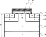
本実施形態の半導体装置は、p型のSiC領域と、p型のSiC領域上に設けられたゲート絶縁膜と、ゲート絶縁膜上に設けられ、p型不純物と3C−SiCを含むゲート電極と、を備える。
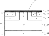
本実施形態の半導体装置は、ゲート電極が3C−SiCと金属との積層構造である点以外は、第1の実施形態と同様である。また、本実施形態の半導体装置の製造方法は、ゲート電極の形成方法以外は、第1の実施形態と同様である。したがって、第1の実施形態と重複する内容については、記述を省略する。
本実施形態の半導体装置は、トレンチゲート構造のMOSFETである点で第1の実施形態と異なる。第1の実施形態と重複する内容については記述を省略する。
本実施形態の半導体装置は、IGBT(Inulated Gate Bipolar Transistor)である点で第1の実施形態と異なる。第1の実施形態と重複する内容については記述を省略する。
17 シリコン膜
18 ゲート電極
26 ウェル領域(p型のSiC領域)
116 ゲート絶縁膜
118 ゲート電極
126 ベース領域(p型のSiC領域)
100 MOSFET(半導体装置)
200 MOSFET(半導体装置)
300 MOSFET(半導体装置)
400 IGBT(半導体装置)
Claims (8)
- p型のSiC領域と、
前記p型のSiC領域の上に設けられたゲート絶縁膜と、
前記ゲート絶縁膜の上に設けられ、p型不純物と3C−SiCを含むゲート電極と、
を備え、
前記ゲート電極の中の前記3C−SiCの体積が、前記ゲート電極の中の4H−SiCの体積よりも大きい半導体装置。 - 前記ゲート電極は、少なくとも前記ゲート絶縁膜と接する領域に、前記p型不純物と前記3C−SiCを含む請求項1記載の半導体装置。
- 前記p型のSiC領域は4H−SiCである請求項1又は請求項2記載の半導体装置。
- 前記p型不純物はアルミニウム(Al)、ガリウム(Ga)又はインジウム(In)である請求項1乃至請求項3いずれか一項記載の半導体装置。
- 前記ゲート電極の中の前記p型不純物の濃度が1×1019cm−3以上である請求項1乃至請求項4いずれか一項記載の半導体装置。
- 前記p型のSiC領域の中のp型不純物の濃度が1×1018cm−3以下である請求項1乃至請求項5いずれか一項記載の半導体装置。
- 前記3C−SiCは、金属化した3C−SiCである請求項1乃至請求項6いずれか一項記載の半導体装置。
- 前記ゲート絶縁膜はシリコン酸化膜である請求項1乃至請求項7いずれか一項記載の半導体装置。
Priority Applications (3)
| Application Number | Priority Date | Filing Date | Title |
|---|---|---|---|
| JP2015179037A JP6526528B2 (ja) | 2015-09-11 | 2015-09-11 | 半導体装置 |
| US15/252,493 US20170077240A1 (en) | 2015-09-11 | 2016-08-31 | Semiconductor device and method for manufacturing the same |
| US16/782,826 US11450745B2 (en) | 2015-09-11 | 2020-02-05 | Semiconductor device and method for manufacturing the same |
Applications Claiming Priority (1)
| Application Number | Priority Date | Filing Date | Title |
|---|---|---|---|
| JP2015179037A JP6526528B2 (ja) | 2015-09-11 | 2015-09-11 | 半導体装置 |
Publications (2)
| Publication Number | Publication Date |
|---|---|
| JP2017055003A JP2017055003A (ja) | 2017-03-16 |
| JP6526528B2 true JP6526528B2 (ja) | 2019-06-05 |
Family
ID=58237190
Family Applications (1)
| Application Number | Title | Priority Date | Filing Date |
|---|---|---|---|
| JP2015179037A Active JP6526528B2 (ja) | 2015-09-11 | 2015-09-11 | 半導体装置 |
Country Status (2)
| Country | Link |
|---|---|
| US (2) | US20170077240A1 (ja) |
| JP (1) | JP6526528B2 (ja) |
Families Citing this family (7)
| Publication number | Priority date | Publication date | Assignee | Title |
|---|---|---|---|---|
| JP6478884B2 (ja) | 2015-09-11 | 2019-03-06 | 株式会社東芝 | 半導体装置 |
| JP6523885B2 (ja) | 2015-09-11 | 2019-06-05 | 株式会社東芝 | 半導体装置 |
| JP7201336B2 (ja) | 2017-05-17 | 2023-01-10 | ローム株式会社 | 半導体装置 |
| DE212018000102U1 (de) | 2017-05-17 | 2019-08-05 | Rohm Co., Ltd. | Halbleitervorrichtung |
| US20190390555A1 (en) * | 2018-06-22 | 2019-12-26 | United Technologies Corporation | Composite airfoil with cleft in platform |
| CN109443295B (zh) * | 2018-10-28 | 2020-11-06 | 北京工业大学 | 一种用于汽车级IGBT芯片表面Al金属化层粗糙度的测试方法 |
| CN114420758B (zh) * | 2021-12-08 | 2023-02-03 | 西安理工大学 | 具有高阈值电压的SiC MOSFET及制造方法 |
Family Cites Families (15)
| Publication number | Priority date | Publication date | Assignee | Title |
|---|---|---|---|---|
| JPS59203799A (ja) | 1983-04-28 | 1984-11-17 | Sharp Corp | 炭化珪素単結晶基板の製造方法 |
| JPH04139014A (ja) * | 1990-09-28 | 1992-05-13 | Toshiba Corp | 炭化珪素の製造方法 |
| WO2001093339A1 (en) * | 2000-05-31 | 2001-12-06 | Matsushita Electric Industrial Co. Ltd. | Misfet |
| US7638841B2 (en) * | 2003-05-20 | 2009-12-29 | Fairchild Semiconductor Corporation | Power semiconductor devices and methods of manufacture |
| JP2005175357A (ja) * | 2003-12-15 | 2005-06-30 | Nissan Motor Co Ltd | 半導体装置とその製造方法 |
| US20050012143A1 (en) * | 2003-06-24 | 2005-01-20 | Hideaki Tanaka | Semiconductor device and method of manufacturing the same |
| JP3711989B2 (ja) | 2003-06-24 | 2005-11-02 | 日産自動車株式会社 | 半導体装置およびその製造方法 |
| US8198675B2 (en) * | 2006-11-21 | 2012-06-12 | Sumitomo Electric Industries, Ltd. | Silicon carbide semiconductor device and method of manufacturing the same |
| JP5721351B2 (ja) * | 2009-07-21 | 2015-05-20 | ローム株式会社 | 半導体装置 |
| JP5558392B2 (ja) * | 2011-03-10 | 2014-07-23 | 株式会社東芝 | 半導体装置とその製造方法 |
| JP5777455B2 (ja) * | 2011-09-08 | 2015-09-09 | 株式会社東芝 | 半導体装置および半導体装置の製造方法 |
| JP6407271B2 (ja) * | 2013-07-02 | 2018-10-17 | ウルトラテック インク | 格子転位を除去するための急速熱処理によるヘテロエピタキシャル層の形成方法および材料処理装置 |
| US9673047B2 (en) * | 2014-10-22 | 2017-06-06 | The United States Of America, As Represented By The Secretary Of The Navy | Solid phase epitaxy of 3C—SiC on Si(001) |
| JP6478884B2 (ja) | 2015-09-11 | 2019-03-06 | 株式会社東芝 | 半導体装置 |
| JP6523885B2 (ja) | 2015-09-11 | 2019-06-05 | 株式会社東芝 | 半導体装置 |
-
2015
- 2015-09-11 JP JP2015179037A patent/JP6526528B2/ja active Active
-
2016
- 2016-08-31 US US15/252,493 patent/US20170077240A1/en not_active Abandoned
-
2020
- 2020-02-05 US US16/782,826 patent/US11450745B2/en active Active
Also Published As
| Publication number | Publication date |
|---|---|
| US20170077240A1 (en) | 2017-03-16 |
| US20200176571A1 (en) | 2020-06-04 |
| JP2017055003A (ja) | 2017-03-16 |
| US11450745B2 (en) | 2022-09-20 |
Similar Documents
| Publication | Publication Date | Title |
|---|---|---|
| JP6526528B2 (ja) | 半導体装置 | |
| JP6478884B2 (ja) | 半導体装置 | |
| JP6058170B2 (ja) | 炭化珪素半導体装置 | |
| JP6180978B2 (ja) | 半導体装置およびその製造方法 | |
| US10672882B2 (en) | Semiconductor device | |
| CN104064586B (zh) | 半导体装置及其制造方法 | |
| JP6478862B2 (ja) | 半導体装置 | |
| WO2010116575A1 (ja) | 半導体装置および半導体装置の製造方法 | |
| JP2012243966A (ja) | 半導体装置 | |
| JP7358590B2 (ja) | 半導体装置 | |
| US10707306B2 (en) | Semiconductor device and method of manufacturing the same | |
| JP2015103631A (ja) | 炭化珪素半導体装置および炭化珪素半導体装置の製造方法 | |
| JP6246613B2 (ja) | 半導体装置およびその製造方法 | |
| TW201711186A (zh) | 半導體裝置 | |
| JP2014222735A (ja) | 半導体装置及びその製造方法 | |
| CN111987163A (zh) | 基于碳化硅的电子器件及其制造方法 | |
| JP6946824B2 (ja) | 半導体装置および半導体装置の製造方法 | |
| JP7577635B2 (ja) | 半導体装置及び半導体装置の製造方法 | |
| JP6164062B2 (ja) | 炭化珪素半導体装置の製造方法 | |
| JP7589125B2 (ja) | 半導体装置及び半導体装置の製造方法 | |
| JP6606020B2 (ja) | 半導体装置、インバータ回路、駆動装置、車両、及び、昇降機 | |
| JP2014222734A (ja) | 半導体装置及びその製造方法 | |
| JP5602256B2 (ja) | 半導体装置の製造方法 |
Legal Events
| Date | Code | Title | Description |
|---|---|---|---|
| A621 | Written request for application examination |
Free format text: JAPANESE INTERMEDIATE CODE: A621 Effective date: 20180206 |
|
| A977 | Report on retrieval |
Free format text: JAPANESE INTERMEDIATE CODE: A971007 Effective date: 20181119 |
|
| A131 | Notification of reasons for refusal |
Free format text: JAPANESE INTERMEDIATE CODE: A131 Effective date: 20181127 |
|
| A521 | Request for written amendment filed |
Free format text: JAPANESE INTERMEDIATE CODE: A523 Effective date: 20190104 |
|
| TRDD | Decision of grant or rejection written | ||
| A01 | Written decision to grant a patent or to grant a registration (utility model) |
Free format text: JAPANESE INTERMEDIATE CODE: A01 Effective date: 20190409 |
|
| A61 | First payment of annual fees (during grant procedure) |
Free format text: JAPANESE INTERMEDIATE CODE: A61 Effective date: 20190508 |
|
| R151 | Written notification of patent or utility model registration |
Ref document number: 6526528 Country of ref document: JP Free format text: JAPANESE INTERMEDIATE CODE: R151 |