JP6521837B2 - ウエーハの加工方法 - Google Patents
ウエーハの加工方法 Download PDFInfo
- Publication number
- JP6521837B2 JP6521837B2 JP2015217351A JP2015217351A JP6521837B2 JP 6521837 B2 JP6521837 B2 JP 6521837B2 JP 2015217351 A JP2015217351 A JP 2015217351A JP 2015217351 A JP2015217351 A JP 2015217351A JP 6521837 B2 JP6521837 B2 JP 6521837B2
- Authority
- JP
- Japan
- Prior art keywords
- wafer
- modified layer
- planned
- line
- dividing line
- Prior art date
- Legal status (The legal status is an assumption and is not a legal conclusion. Google has not performed a legal analysis and makes no representation as to the accuracy of the status listed.)
- Active
Links
Images



Classifications
-
- H—ELECTRICITY
- H10—SEMICONDUCTOR DEVICES; ELECTRIC SOLID-STATE DEVICES NOT OTHERWISE PROVIDED FOR
- H10P—GENERIC PROCESSES OR APPARATUS FOR THE MANUFACTURE OR TREATMENT OF DEVICES COVERED BY CLASS H10
- H10P54/00—Cutting or separating of wafers, substrates or parts of devices
-
- B—PERFORMING OPERATIONS; TRANSPORTING
- B23—MACHINE TOOLS; METAL-WORKING NOT OTHERWISE PROVIDED FOR
- B23K—SOLDERING OR UNSOLDERING; WELDING; CLADDING OR PLATING BY SOLDERING OR WELDING; CUTTING BY APPLYING HEAT LOCALLY, e.g. FLAME CUTTING; WORKING BY LASER BEAM
- B23K26/00—Working by laser beam, e.g. welding, cutting or boring
- B23K26/50—Working by transmitting the laser beam through or within the workpiece
- B23K26/53—Working by transmitting the laser beam through or within the workpiece for modifying or reforming the material inside the workpiece, e.g. for producing break initiation cracks
-
- H—ELECTRICITY
- H10—SEMICONDUCTOR DEVICES; ELECTRIC SOLID-STATE DEVICES NOT OTHERWISE PROVIDED FOR
- H10P—GENERIC PROCESSES OR APPARATUS FOR THE MANUFACTURE OR TREATMENT OF DEVICES COVERED BY CLASS H10
- H10P34/00—Irradiation with electromagnetic or particle radiation of wafers, substrates or parts of devices
- H10P34/40—Irradiation with electromagnetic or particle radiation of wafers, substrates or parts of devices with high-energy radiation
- H10P34/42—Irradiation with electromagnetic or particle radiation of wafers, substrates or parts of devices with high-energy radiation with electromagnetic radiation, e.g. laser annealing
-
- H—ELECTRICITY
- H10—SEMICONDUCTOR DEVICES; ELECTRIC SOLID-STATE DEVICES NOT OTHERWISE PROVIDED FOR
- H10P—GENERIC PROCESSES OR APPARATUS FOR THE MANUFACTURE OR TREATMENT OF DEVICES COVERED BY CLASS H10
- H10P95/00—Generic processes or apparatus for manufacture or treatments not covered by the other groups of this subclass
- H10P95/90—Thermal treatments, e.g. annealing or sintering
-
- H—ELECTRICITY
- H10—SEMICONDUCTOR DEVICES; ELECTRIC SOLID-STATE DEVICES NOT OTHERWISE PROVIDED FOR
- H10W—GENERIC PACKAGES, INTERCONNECTIONS, CONNECTORS OR OTHER CONSTRUCTIONAL DETAILS OF DEVICES COVERED BY CLASS H10
- H10W10/00—Isolation regions in semiconductor bodies between components of integrated devices
- H10W10/01—Manufacture or treatment
-
- B—PERFORMING OPERATIONS; TRANSPORTING
- B23—MACHINE TOOLS; METAL-WORKING NOT OTHERWISE PROVIDED FOR
- B23K—SOLDERING OR UNSOLDERING; WELDING; CLADDING OR PLATING BY SOLDERING OR WELDING; CUTTING BY APPLYING HEAT LOCALLY, e.g. FLAME CUTTING; WORKING BY LASER BEAM
- B23K2103/00—Materials to be soldered, welded or cut
- B23K2103/50—Inorganic materials other than metals or composite materials
- B23K2103/56—Inorganic materials other than metals or composite materials being semiconducting
Landscapes
- Engineering & Computer Science (AREA)
- Physics & Mathematics (AREA)
- Optics & Photonics (AREA)
- Chemical Kinetics & Catalysis (AREA)
- General Chemical & Material Sciences (AREA)
- Oil, Petroleum & Natural Gas (AREA)
- Chemical & Material Sciences (AREA)
- Plasma & Fusion (AREA)
- Mechanical Engineering (AREA)
- Dicing (AREA)
- Laser Beam Processing (AREA)
- Electromagnetism (AREA)
- Mechanical Treatment Of Semiconductor (AREA)
Description
波長 :1342nm
繰り返し周波数 :50kHz
平均出力 :0.5W
集光スポット径 :φ3μm
加工送り速度 :200mm/s
13a 第1分割予定ライン
13b 第2分割予定ライン
15 デバイス
17 第1方向改質層
19 第2方向改質層
24 チャックテーブル
27 ヒーター
31 熱風
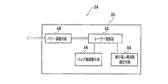
34 レーザービーム照射ユニット
35 レーザービーム発生ユニット
38 集光器(レーザーヘッド)
40 撮像ユニット
50 分割装置
Claims (2)
- 第1の方向に形成された複数の第1分割予定ラインと該第1の方向と交差する第2の方向に形成された複数の第2分割予定ラインとで区画された各領域にデバイスが形成され、該第1分割予定ラインと該第2分割予定ラインのうち少なくとも該第2分割予定ラインが非連続に形成されているウエーハを個々のデバイスチップに分割するウエーハの加工方法であって、
該第1分割予定ラインに沿って、ウエーハに対し透過性を有する波長のレーザービームをウエーハの裏面側からウエーハの内部に集光して照射し、ウエーハの内部に該第1分割予定ラインに沿った複数層の第1方向改質層を形成する第1方向改質層形成ステップと、
該第1方向改質層形成ステップを実施した後、該第2分割予定ラインに沿って、ウエーハに対し透過性を有する波長のレーザービームをウエーハの裏面側からウエーハの内部に集光して照射し、ウエーハの内部に該第2分割予定ラインに沿った複数層の第2方向改質層を形成する第2方向改質層形成ステップと、
該第1方向改質層形成ステップ及び該第2方向改質層形成ステップを実施した後、ウエーハに外力を付与し、該第1方向改質層及び該第2方向改質層を破断起点にウエーハを該第1分割予定ライン及び該第2分割予定ラインに沿って破断して個々のデバイスチップに分割する分割ステップと、を備え、
該第2方向改質層形成ステップは、該第1方向改質層が形成された該第1分割予定ラインにT字路となって交わる該第2分割予定ラインの内部に第2方向改質層を形成するT字路加工ステップを含み、
該T字路加工ステップは、少なくとも該第1分割予定ラインと該第2分割予定ラインとの交点近傍を加熱して、該T字路加工ステップで照射するレーザービームの吸収性を向上させる加熱ステップを含むことを特徴とするウエーハの加工方法。 - 該加熱ステップで加熱する温度は50℃〜120℃に設定される請求項1記載のウエーハの加工方法。
Priority Applications (4)
| Application Number | Priority Date | Filing Date | Title |
|---|---|---|---|
| JP2015217351A JP6521837B2 (ja) | 2015-11-05 | 2015-11-05 | ウエーハの加工方法 |
| TW105132384A TWI694507B (zh) | 2015-11-05 | 2016-10-06 | 晶圓的加工方法 |
| CN201610951897.5A CN107030404B (zh) | 2015-11-05 | 2016-10-27 | 晶片的加工方法 |
| KR1020160141846A KR102424648B1 (ko) | 2015-11-05 | 2016-10-28 | 웨이퍼의 가공 방법 |
Applications Claiming Priority (1)
| Application Number | Priority Date | Filing Date | Title |
|---|---|---|---|
| JP2015217351A JP6521837B2 (ja) | 2015-11-05 | 2015-11-05 | ウエーハの加工方法 |
Publications (2)
| Publication Number | Publication Date |
|---|---|
| JP2017092126A JP2017092126A (ja) | 2017-05-25 |
| JP6521837B2 true JP6521837B2 (ja) | 2019-05-29 |
Family
ID=58739863
Family Applications (1)
| Application Number | Title | Priority Date | Filing Date |
|---|---|---|---|
| JP2015217351A Active JP6521837B2 (ja) | 2015-11-05 | 2015-11-05 | ウエーハの加工方法 |
Country Status (4)
| Country | Link |
|---|---|
| JP (1) | JP6521837B2 (ja) |
| KR (1) | KR102424648B1 (ja) |
| CN (1) | CN107030404B (ja) |
| TW (1) | TWI694507B (ja) |
Families Citing this family (1)
| Publication number | Priority date | Publication date | Assignee | Title |
|---|---|---|---|---|
| JP7177180B2 (ja) * | 2018-12-28 | 2022-11-22 | 株式会社フジクラ | 光透過性部品の製造方法、及び、光透過性部品の製造システム |
Family Cites Families (19)
| Publication number | Priority date | Publication date | Assignee | Title |
|---|---|---|---|---|
| JPH10305420A (ja) | 1997-03-04 | 1998-11-17 | Ngk Insulators Ltd | 酸化物単結晶からなる母材の加工方法、機能性デバイスの製造方法 |
| US6211488B1 (en) * | 1998-12-01 | 2001-04-03 | Accudyne Display And Semiconductor Systems, Inc. | Method and apparatus for separating non-metallic substrates utilizing a laser initiated scribe |
| KR100400059B1 (ko) * | 2000-10-10 | 2003-09-29 | 삼성전자주식회사 | 비금속 기판 절단 장치 및 그 절단 방법 |
| JP4659300B2 (ja) * | 2000-09-13 | 2011-03-30 | 浜松ホトニクス株式会社 | レーザ加工方法及び半導体チップの製造方法 |
| JP3408805B2 (ja) | 2000-09-13 | 2003-05-19 | 浜松ホトニクス株式会社 | 切断起点領域形成方法及び加工対象物切断方法 |
| JP2003088973A (ja) * | 2001-09-12 | 2003-03-25 | Hamamatsu Photonics Kk | レーザ加工方法 |
| JP4656888B2 (ja) * | 2003-08-07 | 2011-03-23 | パナソニック株式会社 | 基板の分割方法 |
| CN100536108C (zh) * | 2005-11-16 | 2009-09-02 | 株式会社电装 | 半导体器件和半导体基板切分方法 |
| JP2007142001A (ja) * | 2005-11-16 | 2007-06-07 | Denso Corp | レーザ加工装置およびレーザ加工方法 |
| JP4793128B2 (ja) * | 2006-06-23 | 2011-10-12 | 株式会社デンソー | 半導体装置の製造装置及び半導体装置の製造方法 |
| JP2010123723A (ja) | 2008-11-19 | 2010-06-03 | Disco Abrasive Syst Ltd | ウエーハのレーザー加工方法 |
| JP2011035253A (ja) * | 2009-08-04 | 2011-02-17 | Disco Abrasive Syst Ltd | ウエーハの加工方法 |
| JP2011061043A (ja) * | 2009-09-10 | 2011-03-24 | Disco Abrasive Syst Ltd | 加工方法および半導体デバイスの製造方法 |
| JP5441629B2 (ja) * | 2009-11-13 | 2014-03-12 | 株式会社ディスコ | ウエーハの加工方法 |
| JP2011108708A (ja) * | 2009-11-13 | 2011-06-02 | Disco Abrasive Syst Ltd | ウエーハの加工方法 |
| JP5558128B2 (ja) * | 2010-02-05 | 2014-07-23 | 株式会社ディスコ | 光デバイスウエーハの加工方法 |
| JP2011233641A (ja) * | 2010-04-26 | 2011-11-17 | Disco Abrasive Syst Ltd | 板状物のレーザー加工方法 |
| JP5597051B2 (ja) * | 2010-07-21 | 2014-10-01 | 浜松ホトニクス株式会社 | レーザ加工方法 |
| JP6062315B2 (ja) * | 2013-04-24 | 2017-01-18 | 株式会社ディスコ | ウエーハの加工方法 |
-
2015
- 2015-11-05 JP JP2015217351A patent/JP6521837B2/ja active Active
-
2016
- 2016-10-06 TW TW105132384A patent/TWI694507B/zh active
- 2016-10-27 CN CN201610951897.5A patent/CN107030404B/zh active Active
- 2016-10-28 KR KR1020160141846A patent/KR102424648B1/ko active Active
Also Published As
| Publication number | Publication date |
|---|---|
| TW201729270A (zh) | 2017-08-16 |
| KR102424648B1 (ko) | 2022-07-25 |
| JP2017092126A (ja) | 2017-05-25 |
| CN107030404A (zh) | 2017-08-11 |
| KR20170053111A (ko) | 2017-05-15 |
| TWI694507B (zh) | 2020-05-21 |
| CN107030404B (zh) | 2020-01-31 |
Similar Documents
| Publication | Publication Date | Title |
|---|---|---|
| JP6504977B2 (ja) | ウエーハの加工方法 | |
| JP6308919B2 (ja) | ウエーハの加工方法 | |
| JP2017092129A (ja) | ウエーハの加工方法 | |
| JP2016054205A (ja) | ウエーハの加工方法 | |
| JP2016042516A (ja) | ウエーハの加工方法 | |
| JP2016076520A (ja) | ウエーハの加工方法 | |
| JP6576211B2 (ja) | ウエーハの加工方法 | |
| JP2016076523A (ja) | ウエーハの加工方法 | |
| JP6308913B2 (ja) | ウエーハの加工方法 | |
| JP6525840B2 (ja) | ウエーハの加工方法 | |
| JP6521837B2 (ja) | ウエーハの加工方法 | |
| JP2017059686A (ja) | ウエーハの加工方法 | |
| JP6293017B2 (ja) | ウエーハの加工方法 | |
| JP6576212B2 (ja) | ウエーハの加工方法 | |
| JP2017059688A (ja) | ウエーハ | |
| JP6532366B2 (ja) | ウエーハの加工方法 | |
| JP2016058429A (ja) | ウエーハの加工方法 | |
| JP6529404B2 (ja) | ウエーハの加工方法 | |
| JP6525833B2 (ja) | ウエーハの加工方法 | |
| JP2016058430A (ja) | ウエーハの加工方法 | |
| JP2017059685A (ja) | ウエーハの加工方法 | |
| JP2016058431A (ja) | ウエーハの加工方法 | |
| JP2016054206A (ja) | ウエーハの加工方法 | |
| JP2016072278A (ja) | ウエーハの加工方法 | |
| JP2016072276A (ja) | ウエーハの加工方法 |
Legal Events
| Date | Code | Title | Description |
|---|---|---|---|
| A621 | Written request for application examination |
Free format text: JAPANESE INTERMEDIATE CODE: A621 Effective date: 20180928 |
|
| TRDD | Decision of grant or rejection written | ||
| A01 | Written decision to grant a patent or to grant a registration (utility model) |
Free format text: JAPANESE INTERMEDIATE CODE: A01 Effective date: 20190423 |
|
| A977 | Report on retrieval |
Free format text: JAPANESE INTERMEDIATE CODE: A971007 Effective date: 20190426 |
|
| A61 | First payment of annual fees (during grant procedure) |
Free format text: JAPANESE INTERMEDIATE CODE: A61 Effective date: 20190423 |
|
| R150 | Certificate of patent or registration of utility model |
Ref document number: 6521837 Country of ref document: JP Free format text: JAPANESE INTERMEDIATE CODE: R150 |
|
| R250 | Receipt of annual fees |
Free format text: JAPANESE INTERMEDIATE CODE: R250 |
|
| R250 | Receipt of annual fees |
Free format text: JAPANESE INTERMEDIATE CODE: R250 |
|
| R250 | Receipt of annual fees |
Free format text: JAPANESE INTERMEDIATE CODE: R250 |
|
| R250 | Receipt of annual fees |
Free format text: JAPANESE INTERMEDIATE CODE: R250 |