JP6528366B2 - 縦型トレンチmosfetの製造方法 - Google Patents
縦型トレンチmosfetの製造方法 Download PDFInfo
- Publication number
- JP6528366B2 JP6528366B2 JP2014140520A JP2014140520A JP6528366B2 JP 6528366 B2 JP6528366 B2 JP 6528366B2 JP 2014140520 A JP2014140520 A JP 2014140520A JP 2014140520 A JP2014140520 A JP 2014140520A JP 6528366 B2 JP6528366 B2 JP 6528366B2
- Authority
- JP
- Japan
- Prior art keywords
- insulating film
- gate insulating
- semiconductor layer
- gate
- manufacturing
- Prior art date
- Legal status (The legal status is an assumption and is not a legal conclusion. Google has not performed a legal analysis and makes no representation as to the accuracy of the status listed.)
- Active
Links
Images



Classifications
-
- H—ELECTRICITY
- H10—SEMICONDUCTOR DEVICES; ELECTRIC SOLID-STATE DEVICES NOT OTHERWISE PROVIDED FOR
- H10D—INORGANIC ELECTRIC SEMICONDUCTOR DEVICES
- H10D30/00—Field-effect transistors [FET]
- H10D30/60—Insulated-gate field-effect transistors [IGFET]
-
- H—ELECTRICITY
- H10—SEMICONDUCTOR DEVICES; ELECTRIC SOLID-STATE DEVICES NOT OTHERWISE PROVIDED FOR
- H10D—INORGANIC ELECTRIC SEMICONDUCTOR DEVICES
- H10D30/00—Field-effect transistors [FET]
- H10D30/01—Manufacture or treatment
-
- H—ELECTRICITY
- H10—SEMICONDUCTOR DEVICES; ELECTRIC SOLID-STATE DEVICES NOT OTHERWISE PROVIDED FOR
- H10D—INORGANIC ELECTRIC SEMICONDUCTOR DEVICES
- H10D30/00—Field-effect transistors [FET]
- H10D30/01—Manufacture or treatment
- H10D30/021—Manufacture or treatment of FETs having insulated gates [IGFET]
-
- H—ELECTRICITY
- H10—SEMICONDUCTOR DEVICES; ELECTRIC SOLID-STATE DEVICES NOT OTHERWISE PROVIDED FOR
- H10D—INORGANIC ELECTRIC SEMICONDUCTOR DEVICES
- H10D30/00—Field-effect transistors [FET]
- H10D30/01—Manufacture or treatment
- H10D30/021—Manufacture or treatment of FETs having insulated gates [IGFET]
- H10D30/028—Manufacture or treatment of FETs having insulated gates [IGFET] of double-diffused metal oxide semiconductor [DMOS] FETs
- H10D30/0291—Manufacture or treatment of FETs having insulated gates [IGFET] of double-diffused metal oxide semiconductor [DMOS] FETs of vertical DMOS [VDMOS] FETs
- H10D30/0297—Manufacture or treatment of FETs having insulated gates [IGFET] of double-diffused metal oxide semiconductor [DMOS] FETs of vertical DMOS [VDMOS] FETs using recessing of the gate electrodes, e.g. to form trench gate electrodes
-
- H—ELECTRICITY
- H10—SEMICONDUCTOR DEVICES; ELECTRIC SOLID-STATE DEVICES NOT OTHERWISE PROVIDED FOR
- H10D—INORGANIC ELECTRIC SEMICONDUCTOR DEVICES
- H10D30/00—Field-effect transistors [FET]
- H10D30/60—Insulated-gate field-effect transistors [IGFET]
- H10D30/601—Insulated-gate field-effect transistors [IGFET] having lightly-doped drain or source extensions, e.g. LDD IGFETs or DDD IGFETs
- H10D30/603—Insulated-gate field-effect transistors [IGFET] having lightly-doped drain or source extensions, e.g. LDD IGFETs or DDD IGFETs having asymmetry in the channel direction, e.g. lateral high-voltage MISFETs having drain offset region or extended drain IGFETs [EDMOS]
-
- H—ELECTRICITY
- H10—SEMICONDUCTOR DEVICES; ELECTRIC SOLID-STATE DEVICES NOT OTHERWISE PROVIDED FOR
- H10D—INORGANIC ELECTRIC SEMICONDUCTOR DEVICES
- H10D30/00—Field-effect transistors [FET]
- H10D30/60—Insulated-gate field-effect transistors [IGFET]
- H10D30/64—Double-diffused metal-oxide semiconductor [DMOS] FETs
- H10D30/66—Vertical DMOS [VDMOS] FETs
- H10D30/668—Vertical DMOS [VDMOS] FETs having trench gate electrodes, e.g. UMOS transistors
-
- H—ELECTRICITY
- H10—SEMICONDUCTOR DEVICES; ELECTRIC SOLID-STATE DEVICES NOT OTHERWISE PROVIDED FOR
- H10D—INORGANIC ELECTRIC SEMICONDUCTOR DEVICES
- H10D62/00—Semiconductor bodies, or regions thereof, of devices having potential barriers
- H10D62/80—Semiconductor bodies, or regions thereof, of devices having potential barriers characterised by the materials
- H10D62/85—Semiconductor bodies, or regions thereof, of devices having potential barriers characterised by the materials being Group III-V materials, e.g. GaAs
- H10D62/8503—Nitride Group III-V materials, e.g. AlN or GaN
-
- H—ELECTRICITY
- H10—SEMICONDUCTOR DEVICES; ELECTRIC SOLID-STATE DEVICES NOT OTHERWISE PROVIDED FOR
- H10D—INORGANIC ELECTRIC SEMICONDUCTOR DEVICES
- H10D64/00—Electrodes of devices having potential barriers
- H10D64/01—Manufacture or treatment
- H10D64/013—Manufacture or treatment of electrodes having a conductor capacitively coupled to a semiconductor by an insulator
- H10D64/01358—Manufacture or treatment of electrodes having a conductor capacitively coupled to a semiconductor by an insulator the insulator being formed after the semiconductor body, the semiconductor being a Group III-V material
-
- H—ELECTRICITY
- H10—SEMICONDUCTOR DEVICES; ELECTRIC SOLID-STATE DEVICES NOT OTHERWISE PROVIDED FOR
- H10D—INORGANIC ELECTRIC SEMICONDUCTOR DEVICES
- H10D64/00—Electrodes of devices having potential barriers
- H10D64/118—Electrodes comprising insulating layers having particular dielectric or electrostatic properties, e.g. having static charges
-
- H—ELECTRICITY
- H10—SEMICONDUCTOR DEVICES; ELECTRIC SOLID-STATE DEVICES NOT OTHERWISE PROVIDED FOR
- H10D—INORGANIC ELECTRIC SEMICONDUCTOR DEVICES
- H10D64/00—Electrodes of devices having potential barriers
- H10D64/20—Electrodes characterised by their shapes, relative sizes or dispositions
- H10D64/27—Electrodes not carrying the current to be rectified, amplified, oscillated or switched, e.g. gates
- H10D64/311—Gate electrodes for field-effect devices
- H10D64/411—Gate electrodes for field-effect devices for FETs
- H10D64/511—Gate electrodes for field-effect devices for FETs for IGFETs
- H10D64/512—Disposition of the gate electrodes, e.g. buried gates
- H10D64/513—Disposition of the gate electrodes, e.g. buried gates within recesses in the substrate, e.g. trench gates, groove gates or buried gates
-
- H—ELECTRICITY
- H10—SEMICONDUCTOR DEVICES; ELECTRIC SOLID-STATE DEVICES NOT OTHERWISE PROVIDED FOR
- H10D—INORGANIC ELECTRIC SEMICONDUCTOR DEVICES
- H10D64/00—Electrodes of devices having potential barriers
- H10D64/60—Electrodes characterised by their materials
- H10D64/66—Electrodes having a conductor capacitively coupled to a semiconductor by an insulator, e.g. MIS electrodes
- H10D64/68—Electrodes having a conductor capacitively coupled to a semiconductor by an insulator, e.g. MIS electrodes characterised by the insulator, e.g. by the gate insulator
- H10D64/681—Electrodes having a conductor capacitively coupled to a semiconductor by an insulator, e.g. MIS electrodes characterised by the insulator, e.g. by the gate insulator having a compositional variation, e.g. multilayered
- H10D64/685—Electrodes having a conductor capacitively coupled to a semiconductor by an insulator, e.g. MIS electrodes characterised by the insulator, e.g. by the gate insulator having a compositional variation, e.g. multilayered being perpendicular to the channel plane
-
- H—ELECTRICITY
- H10—SEMICONDUCTOR DEVICES; ELECTRIC SOLID-STATE DEVICES NOT OTHERWISE PROVIDED FOR
- H10P—GENERIC PROCESSES OR APPARATUS FOR THE MANUFACTURE OR TREATMENT OF DEVICES COVERED BY CLASS H10
- H10P14/00—Formation of materials, e.g. in the shape of layers or pillars
- H10P14/60—Formation of materials, e.g. in the shape of layers or pillars of insulating materials
- H10P14/63—Formation of materials, e.g. in the shape of layers or pillars of insulating materials characterised by the formation processes
- H10P14/6326—Deposition processes
- H10P14/6328—Deposition from the gas or vapour phase
- H10P14/6334—Deposition from the gas or vapour phase using decomposition or reaction of gaseous or vapour phase compounds, i.e. chemical vapour deposition
- H10P14/6336—Deposition from the gas or vapour phase using decomposition or reaction of gaseous or vapour phase compounds, i.e. chemical vapour deposition in the presence of a plasma [PECVD]
-
- H—ELECTRICITY
- H10—SEMICONDUCTOR DEVICES; ELECTRIC SOLID-STATE DEVICES NOT OTHERWISE PROVIDED FOR
- H10P—GENERIC PROCESSES OR APPARATUS FOR THE MANUFACTURE OR TREATMENT OF DEVICES COVERED BY CLASS H10
- H10P14/00—Formation of materials, e.g. in the shape of layers or pillars
- H10P14/60—Formation of materials, e.g. in the shape of layers or pillars of insulating materials
- H10P14/63—Formation of materials, e.g. in the shape of layers or pillars of insulating materials characterised by the formation processes
- H10P14/6326—Deposition processes
- H10P14/6328—Deposition from the gas or vapour phase
- H10P14/6334—Deposition from the gas or vapour phase using decomposition or reaction of gaseous or vapour phase compounds, i.e. chemical vapour deposition
- H10P14/6339—Deposition from the gas or vapour phase using decomposition or reaction of gaseous or vapour phase compounds, i.e. chemical vapour deposition deposition by cyclic CVD, e.g. ALD, ALE or pulsed CVD
-
- H—ELECTRICITY
- H10—SEMICONDUCTOR DEVICES; ELECTRIC SOLID-STATE DEVICES NOT OTHERWISE PROVIDED FOR
- H10P—GENERIC PROCESSES OR APPARATUS FOR THE MANUFACTURE OR TREATMENT OF DEVICES COVERED BY CLASS H10
- H10P14/00—Formation of materials, e.g. in the shape of layers or pillars
- H10P14/60—Formation of materials, e.g. in the shape of layers or pillars of insulating materials
- H10P14/66—Formation of materials, e.g. in the shape of layers or pillars of insulating materials characterised by the type of materials
- H10P14/662—Laminate layers, e.g. stacks of alternating high-k metal oxides
-
- H—ELECTRICITY
- H10—SEMICONDUCTOR DEVICES; ELECTRIC SOLID-STATE DEVICES NOT OTHERWISE PROVIDED FOR
- H10P—GENERIC PROCESSES OR APPARATUS FOR THE MANUFACTURE OR TREATMENT OF DEVICES COVERED BY CLASS H10
- H10P14/00—Formation of materials, e.g. in the shape of layers or pillars
- H10P14/60—Formation of materials, e.g. in the shape of layers or pillars of insulating materials
- H10P14/69—Inorganic materials
- H10P14/692—Inorganic materials composed of oxides, glassy oxides or oxide-based glasses
- H10P14/6921—Inorganic materials composed of oxides, glassy oxides or oxide-based glasses containing silicon
- H10P14/6922—Inorganic materials composed of oxides, glassy oxides or oxide-based glasses containing silicon the material containing Si, O and at least one of H, N, C, F or other non-metal elements, e.g. SiOC, SiOC:H or SiONC
-
- H—ELECTRICITY
- H10—SEMICONDUCTOR DEVICES; ELECTRIC SOLID-STATE DEVICES NOT OTHERWISE PROVIDED FOR
- H10D—INORGANIC ELECTRIC SEMICONDUCTOR DEVICES
- H10D64/00—Electrodes of devices having potential barriers
- H10D64/60—Electrodes characterised by their materials
- H10D64/66—Electrodes having a conductor capacitively coupled to a semiconductor by an insulator, e.g. MIS electrodes
- H10D64/68—Electrodes having a conductor capacitively coupled to a semiconductor by an insulator, e.g. MIS electrodes characterised by the insulator, e.g. by the gate insulator
- H10D64/691—Electrodes having a conductor capacitively coupled to a semiconductor by an insulator, e.g. MIS electrodes characterised by the insulator, e.g. by the gate insulator comprising metallic compounds, e.g. metal oxides or metal silicates
Landscapes
- Insulated Gate Type Field-Effect Transistor (AREA)
- Formation Of Insulating Films (AREA)
Description
本発明の第1の形態は、
縦型トレンチMOSFETの製造方法であって、
窒化ガリウム(GaN)から成る半導体層に、ドライエッチングによってトレンチを形成し、
前記ドライエッチングによって損傷した前記半導体層の表面を、TMAHによるウェットエッチングによって除去し、
前記ウェットエッチングが行なわれた前記半導体層の上に、酸化物から主に成る第1のゲート絶縁膜を、オゾンを酸化剤として用いた原子層堆積法によって形成し、
前記第1のゲート絶縁膜の上に、酸化物から主に成る第2のゲート絶縁膜を、酸素プラズマを酸化剤として用いた原子層堆積法によって形成し、
前記第2のゲート絶縁膜の上にゲート電極を形成し、
前記第1のゲート絶縁膜を形成する工程では、以下の工程a1〜a4を繰り返し、
(工程a1)反応室に原料ガスを投入
(工程a2)反応室から原料ガスをパージ
(工程a3)反応室に酸化剤としてオゾンを投入
(工程a4)反応室からオゾンをパージ
前記第2のゲート絶縁膜を形成する工程では、以下の工程b1〜b5を繰り返し、
(工程b1)反応室に原料ガスを投入
(工程b2)反応室から原料ガスをパージ
(工程b3)反応室に酸化剤として酸素を投入
(工程b4)高周波電源によって反応室内にプラズマを生成
(工程b5)反応室から酸素をパージ
前記第1のゲート絶縁膜および前記第2のゲート絶縁膜に対してアニール処理を行うことにより、前記第2のゲート絶縁膜の炭素濃度を、1×10¹⁹原子/cm3未満、かつ前記第1のゲート絶縁膜の水素濃度の低下の幅を、前記第2のゲート絶縁膜側の水素濃度の低下の幅よりも大きくし、前記半導体層のキャリア移動度は10cm2/V・sを超える、縦型トレンチMOSFETの製造方法である。また、本発明は以下の形態として実現することもできる。
A−1.半導体装置の構成
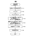
図1は、第1実施形態における半導体装置100の構成を模式的に示す断面図である。半導体装置100は、窒化ガリウム(GaN)を用いて形成されたGaN系の半導体装置である。本実施形態では、半導体装置100は、横型MOSFET(Metal-Oxide-Semiconductor Field-Effect Transistor)である。本実施形態では、半導体装置100は、電力制御に用いられ、パワーデバイスとも呼ばれる。
図2は、第1実施形態における半導体装置100の製造方法を示す工程図である。まず、製造者は、エピタキシャル成長によって、基板110の上にバッファ層111を形成し、その後、バッファ層111の上に半導体層114を形成する(工程P110)。
(工程a1)反応室に原料ガスを投入
(工程a2)反応室から原料ガスをパージ
(工程a3)反応室に酸化剤としてオゾン(O3)を投入
(工程a4)反応室からオゾンをパージ
(工程b1)反応室に原料ガスを投入
(工程b2)反応室から原料ガスをパージ
(工程b3)反応室に酸化剤として酸素(O2)を投入
(工程b4)高周波電源によって反応室内にプラズマを生成
(工程b5)反応室から酸素をパージ
B−1.半導体装置の構成
図3は、第2実施形態における半導体装置200の構成を模式的に示す断面図である。半導体装置200は、窒化ガリウム(GaN)を用いて形成されたGaN系の半導体装置である。本実施形態では、半導体装置200は、縦型トレンチMOSFETである。本実施形態では、半導体装置200は、電力制御に用いられ、パワーデバイスとも呼ばれる。図3には、図1と同様に、XYZ軸が図示されている。
図4は、第2実施形態における半導体装置200の製造方法を示す工程図である。まず、製造者は、エピタキシャル成長によって、基板210の上に半導体層212,214,216を順に形成する(工程P210)。
図5は、第1評価試験に用いた半導体装置300の構成を模式的に示す断面図である。半導体装置300は、窒化ガリウム(GaN)を用いて形成されたGaN系の半導体装置である。半導体装置300の製造方法は、第2実施形態に準ずる。図5には、図1と同様に、XYZ軸が図示されている。
第2のゲート絶縁膜332:50nm
第1のゲート絶縁膜331:0nm
第2のゲート絶縁膜332:40nm
第1のゲート絶縁膜331:10nm
第2のゲート絶縁膜332:45nm
第1のゲート絶縁膜331:5nm
第2のゲート絶縁膜332:0nm
第1のゲート絶縁膜331:50nm
図8は、第2評価試験に用いた試料400の構成を模式的に示す断面図である。図8には、図1と同様に、XYZ軸が図示されている。試料400は、基板410と、第1の絶縁膜431と、第2の絶縁膜432とを備える。
本発明は、上述の実施形態や実施例、変形例に限られるものではなく、その趣旨を逸脱しない範囲において種々の構成で実現することができる。例えば、発明の概要の欄に記載した各形態中の技術的特徴に対応する実施形態、実施例、変形例中の技術的特徴は、上述の課題の一部または全部を解決するために、あるいは、上述の効果の一部または全部を達成するために、適宜、差し替えや、組み合わせを行うことが可能である。また、その技術的特徴が本明細書中に必須なものとして説明されていなければ、適宜、削除することが可能である。
110…基板
111…バッファ層
114,116,117,118…半導体層
121,123…コンタクトホール
130…ゲート絶縁膜
131…第1のゲート絶縁膜
132…第2のゲート絶縁膜
141…ソース電極
142…ゲート電極
143…ドレイン電極
200…半導体装置
210…基板
212,214,216…半導体層
221…コンタクトホール
222…トレンチ
224…リセス
230…ゲート絶縁膜
231…第1のゲート絶縁膜
232…第2のゲート絶縁膜
241…ソース電極
242…ゲート電極
243…ドレイン電極
244…ボディ電極
300…半導体装置
314,316…半導体層
322…トレンチ
324…リセス
330…ゲート絶縁膜
331…第1のゲート絶縁膜
332…第2のゲート絶縁膜
341…ソース電極
342…ゲート電極
343…ドレイン電極
344…ボディ電極
400…試料
410…基板
431…第1の絶縁膜
432…第2の絶縁膜
Claims (9)
- 縦型トレンチMOSFETの製造方法であって、
窒化ガリウム(GaN)から成る半導体層に、ドライエッチングによってトレンチを形成し、
前記ドライエッチングによって損傷した前記半導体層の表面を、TMAHによるウェットエッチングによって除去し、
前記ウェットエッチングが行なわれた前記半導体層の上に、酸化物から主に成る第1のゲート絶縁膜を、オゾンを酸化剤として用いた原子層堆積法によって形成し、
前記第1のゲート絶縁膜の上に、酸化物から主に成る第2のゲート絶縁膜を、酸素プラズマを酸化剤として用いた原子層堆積法によって形成し、
前記第2のゲート絶縁膜の上にゲート電極を形成し、
前記第1のゲート絶縁膜を形成する工程では、以下の工程a1〜a4を繰り返し、
(工程a1)反応室に原料ガスを投入
(工程a2)反応室から原料ガスをパージ
(工程a3)反応室に酸化剤としてオゾンを投入
(工程a4)反応室からオゾンをパージ
前記第2のゲート絶縁膜を形成する工程では、以下の工程b1〜b5を繰り返し、
(工程b1)反応室に原料ガスを投入
(工程b2)反応室から原料ガスをパージ
(工程b3)反応室に酸化剤として酸素を投入
(工程b4)高周波電源によって反応室内にプラズマを生成
(工程b5)反応室から酸素をパージ
前記第1のゲート絶縁膜および前記第2のゲート絶縁膜に対してアニール処理を行うことにより、前記第2のゲート絶縁膜の炭素濃度を、1×10¹⁹原子/cm3未満、かつ前記第1のゲート絶縁膜の水素濃度の低下の幅を、前記第2のゲート絶縁膜側の水素濃度の低下の幅よりも大きくし、前記半導体層のキャリア移動度は10cm2/V・sを超える、縦型トレンチMOSFETの製造方法。 - 2nm以上20nm以下の膜厚で前記第1のゲート絶縁膜を形成する、請求項1に記載の縦型トレンチMOSFETの製造方法。
- 前記第2のゲート絶縁膜を前記第1のゲート絶縁膜より厚く形成する、請求項1または請求項2に記載の縦型トレンチMOSFETの製造方法。
- 請求項1から請求項3までのいずれか一項に記載の縦型トレンチMOSFETの製造方法であって、
前記第1のゲート絶縁膜を形成する前に、前記半導体層の厚さ方向に落ち込んだ溝部を前記半導体層に形成し、
前記第1のゲート絶縁膜および前記第2のゲート絶縁膜を、前記溝部の外側から内側にわたって形成する、縦型トレンチMOSFETの製造方法。 - 前記第1のゲート絶縁膜および前記第2のゲート絶縁膜を形成する際、前記半導体層の温度を200℃以上600℃以下に維持する、請求項1から請求項4までのいずれか一項に記載の縦型トレンチMOSFETの製造方法。
- 2原子%以上30原子%以下のオゾンを含有する酸化剤を用いた原子層堆積法によって前記第1のゲート絶縁膜を形成する、請求項1から請求項5までのいずれか一項に記載の縦型トレンチMOSFETの製造方法。
- 200W以上2000W以下の高周波電源による酸素プラズマを酸化剤として用いた原子層堆積法によって前記第2のゲート絶縁膜を形成する、請求項1から請求項6までのいずれか一項に記載の縦型トレンチMOSFETの製造方法。
- 前記第1のゲート絶縁膜および前記第2のゲート絶縁膜に対して300℃以上900℃以下でアニール処理を行う、請求項1から請求項7までのいずれか一項に記載の縦型トレンチMOSFETの製造方法。
- 前記アニール処理前における前記第2のゲート絶縁膜の炭素濃度は、1×10¹⁹原子/cm3以上であり、
前記アニール処理後における前記第2のゲート絶縁膜の炭素濃度は、1×10¹⁹原子/cm3未満である、請求項1から請求項8までのいずれか一項に記載の縦型トレンチMOSFETの製造方法。
Priority Applications (3)
| Application Number | Priority Date | Filing Date | Title |
|---|---|---|---|
| JP2014140520A JP6528366B2 (ja) | 2014-07-08 | 2014-07-08 | 縦型トレンチmosfetの製造方法 |
| CN201510364222.6A CN105304712B (zh) | 2014-07-08 | 2015-06-26 | 半导体装置及其制造方法 |
| US14/754,435 US9466706B2 (en) | 2014-07-08 | 2015-06-29 | Semiconductor device including first and second gate insulating films disposed on a semiconductor layer and manufacturing method of the same |
Applications Claiming Priority (1)
| Application Number | Priority Date | Filing Date | Title |
|---|---|---|---|
| JP2014140520A JP6528366B2 (ja) | 2014-07-08 | 2014-07-08 | 縦型トレンチmosfetの製造方法 |
Related Child Applications (1)
| Application Number | Title | Priority Date | Filing Date |
|---|---|---|---|
| JP2019023105A Division JP2019071497A (ja) | 2019-02-13 | 2019-02-13 | 半導体装置およびその製造方法 |
Publications (2)
| Publication Number | Publication Date |
|---|---|
| JP2016018888A JP2016018888A (ja) | 2016-02-01 |
| JP6528366B2 true JP6528366B2 (ja) | 2019-06-12 |
Family
ID=55068211
Family Applications (1)
| Application Number | Title | Priority Date | Filing Date |
|---|---|---|---|
| JP2014140520A Active JP6528366B2 (ja) | 2014-07-08 | 2014-07-08 | 縦型トレンチmosfetの製造方法 |
Country Status (3)
| Country | Link |
|---|---|
| US (1) | US9466706B2 (ja) |
| JP (1) | JP6528366B2 (ja) |
| CN (1) | CN105304712B (ja) |
Families Citing this family (19)
| Publication number | Priority date | Publication date | Assignee | Title |
|---|---|---|---|---|
| WO2014185034A1 (ja) * | 2013-05-13 | 2014-11-20 | パナソニックIpマネジメント株式会社 | 半導体装置 |
| JP6226004B2 (ja) * | 2016-02-29 | 2017-11-08 | 富士電機株式会社 | 半導体装置および半導体装置の製造方法 |
| JP6673125B2 (ja) * | 2016-09-30 | 2020-03-25 | 豊田合成株式会社 | 半導体装置 |
| JP6618944B2 (ja) * | 2017-03-10 | 2019-12-11 | 株式会社東芝 | 半導体装置及び電気装置 |
| JP7056408B2 (ja) * | 2017-06-30 | 2022-04-19 | 富士電機株式会社 | 窒化ガリウム系半導体装置および窒化ガリウム系半導体装置の製造方法 |
| JP7388624B2 (ja) * | 2017-12-11 | 2023-11-29 | 出光興産株式会社 | 半導体装置及び半導体装置の製造方法 |
| RU2677500C1 (ru) * | 2018-03-07 | 2019-01-17 | Федеральное государственное бюджетное образовательное учреждение высшего образования "Чеченский государственный университет" | Способ изготовления полупроводникового прибора |
| EP3627559B1 (en) * | 2018-09-19 | 2022-06-22 | Imec Vzw | A iii-v semiconductor device and a method for forming a iii-v semiconductor device comprising an edge termination structure |
| JP7185225B2 (ja) * | 2018-11-22 | 2022-12-07 | 株式会社豊田中央研究所 | 半導体装置および半導体装置の製造方法 |
| CN111668189B (zh) * | 2019-03-07 | 2021-09-21 | 西安电子科技大学 | 一种mis-hemt器件的热电子效应测试结构及其表征方法 |
| JP7450446B2 (ja) | 2020-04-13 | 2024-03-15 | 株式会社アドバンテスト | 半導体装置、半導体装置の製造方法、および試験装置 |
| JP7276247B2 (ja) * | 2020-05-22 | 2023-05-18 | 豊田合成株式会社 | 半導体装置の製造方法 |
| JP7498464B2 (ja) * | 2020-07-07 | 2024-06-12 | 富士電機株式会社 | 窒化物半導体装置の製造方法及び窒化物半導体装置 |
| FR3112422B1 (fr) * | 2020-07-09 | 2022-08-12 | Commissariat Energie Atomique | Procédé de réalisation d’une couche diélectrique sur une structure en matériaux III-V |
| JP7583408B2 (ja) * | 2021-02-25 | 2024-11-14 | 株式会社デンソー | スイッチングデバイスの製造方法 |
| JP7587792B2 (ja) * | 2021-02-25 | 2024-11-21 | 株式会社デンソー | 窒化物半導体装置の製造方法 |
| JP7606190B2 (ja) | 2021-02-25 | 2024-12-25 | 株式会社デンソー | スイッチングデバイスとその製造方法 |
| CN115274923B (zh) * | 2022-07-20 | 2024-10-15 | 无锡松煜科技有限公司 | 一种光伏N型TOPCon电池ALD钝化膜制造工艺 |
| US20240290879A1 (en) * | 2023-02-27 | 2024-08-29 | Globalfoundries U.S. Inc. | Field-effect transistors with deposited gate dielectric layers |
Family Cites Families (22)
| Publication number | Priority date | Publication date | Assignee | Title |
|---|---|---|---|---|
| US4675089A (en) * | 1985-11-25 | 1987-06-23 | At&T Technologies, Inc. | Low temperature deposition method for high quality aluminum oxide films |
| KR100400246B1 (ko) * | 2000-12-29 | 2003-10-01 | 주식회사 하이닉스반도체 | 고집적 디램용 셀 커패시터의 제조방법 |
| JP2004214366A (ja) * | 2002-12-27 | 2004-07-29 | Nec Electronics Corp | 半導体装置及びその製造方法 |
| WO2004093179A1 (ja) * | 2003-04-17 | 2004-10-28 | Fujitsu Limited | 高誘電体膜の形成方法 |
| JP4277268B2 (ja) * | 2003-11-28 | 2009-06-10 | ローム株式会社 | 金属化合物薄膜の製造方法、ならびに当該金属化合物薄膜を含む半導体装置の製造方法 |
| US7067438B2 (en) * | 2004-02-19 | 2006-06-27 | Micron Technology, Inc. | Atomic layer deposition method of forming an oxide comprising layer on a substrate |
| JP3987046B2 (ja) * | 2004-02-24 | 2007-10-03 | 株式会社ルネサステクノロジ | 半導体装置の製造方法 |
| US20070065578A1 (en) * | 2005-09-21 | 2007-03-22 | Applied Materials, Inc. | Treatment processes for a batch ALD reactor |
| KR101014858B1 (ko) * | 2006-03-30 | 2011-02-15 | 미쯔이 죠센 가부시키가이샤 | 플라즈마 원자층 성장 방법 및 장치 |
| JP4789713B2 (ja) * | 2006-06-29 | 2011-10-12 | 株式会社豊田中央研究所 | ウェットエッチング方法、ダメージ層除去方法、半導体装置の製造方法、および半導体基板の製造方法 |
| JP2008028249A (ja) * | 2006-07-24 | 2008-02-07 | Matsushita Electric Ind Co Ltd | 半導体装置及び半導体装置の製造方法 |
| JP2008103408A (ja) | 2006-10-17 | 2008-05-01 | Furukawa Electric Co Ltd:The | 窒化物化合物半導体トランジスタ及びその製造方法 |
| JP2009206312A (ja) | 2008-02-28 | 2009-09-10 | Mitsui Eng & Shipbuild Co Ltd | 成膜方法および成膜装置 |
| JP2010098141A (ja) | 2008-10-16 | 2010-04-30 | Sumitomo Electric Device Innovations Inc | 半導体装置の製造方法 |
| US20130011579A1 (en) * | 2010-11-30 | 2013-01-10 | Air Products And Chemicals, Inc. | Metal-Enolate Precursors For Depositing Metal-Containing Films |
| JP5839804B2 (ja) | 2011-01-25 | 2016-01-06 | 国立大学法人東北大学 | 半導体装置の製造方法、および半導体装置 |
| JP5395309B2 (ja) * | 2011-03-23 | 2014-01-22 | パナソニック株式会社 | 半導体装置およびその製造方法 |
| JP2013074069A (ja) | 2011-09-27 | 2013-04-22 | Fujitsu Ltd | 半導体装置及び半導体装置の製造方法 |
| JP2013140866A (ja) | 2012-01-04 | 2013-07-18 | Renesas Electronics Corp | 半導体装置及び半導体装置の製造方法 |
| WO2013123225A1 (en) * | 2012-02-17 | 2013-08-22 | Applied Materials, Inc. | Passivation film stack for silicon-based solar cells |
| JP5957994B2 (ja) * | 2012-03-16 | 2016-07-27 | 富士通株式会社 | 半導体装置の製造方法 |
| WO2014010405A1 (ja) * | 2012-07-13 | 2014-01-16 | 株式会社村田製作所 | トランジスタおよびトランジスタの製造方法 |
-
2014
- 2014-07-08 JP JP2014140520A patent/JP6528366B2/ja active Active
-
2015
- 2015-06-26 CN CN201510364222.6A patent/CN105304712B/zh active Active
- 2015-06-29 US US14/754,435 patent/US9466706B2/en active Active
Also Published As
| Publication number | Publication date |
|---|---|
| JP2016018888A (ja) | 2016-02-01 |
| US9466706B2 (en) | 2016-10-11 |
| CN105304712B (zh) | 2018-10-16 |
| US20160013282A1 (en) | 2016-01-14 |
| CN105304712A (zh) | 2016-02-03 |
Similar Documents
| Publication | Publication Date | Title |
|---|---|---|
| JP6528366B2 (ja) | 縦型トレンチmosfetの製造方法 | |
| CN106663634B (zh) | 半导体器件及半导体器件的制造方法 | |
| US10153356B2 (en) | Method of manufacturing semiconductor device, and semiconductor device | |
| US9691846B2 (en) | Semiconductor device including an insulating layer which includes negatively charged microcrystal | |
| US9548204B2 (en) | Semiconductor device, manufacturing method of the same and method of suppressing decrease of flat band voltage | |
| US10256323B2 (en) | Method of manufacturing semiconductor device including an n type semiconductor region formed in a p type semiconductor layer | |
| US9905432B2 (en) | Semiconductor device, method for manufacturing the same and power converter | |
| JP6327139B2 (ja) | 半導体装置およびその製造方法 | |
| JP6011620B2 (ja) | トランジスタの製造方法 | |
| US10153352B2 (en) | Semiconductor device | |
| JP6658431B2 (ja) | 半導体装置 | |
| JP2019071497A (ja) | 半導体装置およびその製造方法 | |
| US9831311B2 (en) | Semiconductor device and method of manufacturing the same | |
| US10177234B2 (en) | Semiconductor device | |
| US9852925B2 (en) | Method of manufacturing semiconductor device | |
| US9966447B2 (en) | Method of manufacturing semiconductor device by plasma treatment and heat treatment, and semiconductor device | |
| JP2019067847A (ja) | 半導体装置 | |
| JP2015198210A (ja) | 半導体装置およびその製造方法 |
Legal Events
| Date | Code | Title | Description |
|---|---|---|---|
| A621 | Written request for application examination |
Free format text: JAPANESE INTERMEDIATE CODE: A621 Effective date: 20160823 |
|
| A977 | Report on retrieval |
Free format text: JAPANESE INTERMEDIATE CODE: A971007 Effective date: 20170511 |
|
| A131 | Notification of reasons for refusal |
Free format text: JAPANESE INTERMEDIATE CODE: A131 Effective date: 20170606 |
|
| A521 | Request for written amendment filed |
Free format text: JAPANESE INTERMEDIATE CODE: A523 Effective date: 20170802 |
|
| A131 | Notification of reasons for refusal |
Free format text: JAPANESE INTERMEDIATE CODE: A131 Effective date: 20171219 |
|
| A521 | Request for written amendment filed |
Free format text: JAPANESE INTERMEDIATE CODE: A523 Effective date: 20180214 |
|
| A131 | Notification of reasons for refusal |
Free format text: JAPANESE INTERMEDIATE CODE: A131 Effective date: 20180529 |
|
| A521 | Request for written amendment filed |
Free format text: JAPANESE INTERMEDIATE CODE: A523 Effective date: 20180726 |
|
| A02 | Decision of refusal |
Free format text: JAPANESE INTERMEDIATE CODE: A02 Effective date: 20181113 |
|
| A521 | Request for written amendment filed |
Free format text: JAPANESE INTERMEDIATE CODE: A523 Effective date: 20190213 |
|
| A911 | Transfer to examiner for re-examination before appeal (zenchi) |
Free format text: JAPANESE INTERMEDIATE CODE: A911 Effective date: 20190220 |
|
| TRDD | Decision of grant or rejection written | ||
| A01 | Written decision to grant a patent or to grant a registration (utility model) |
Free format text: JAPANESE INTERMEDIATE CODE: A01 Effective date: 20190416 |
|
| A61 | First payment of annual fees (during grant procedure) |
Free format text: JAPANESE INTERMEDIATE CODE: A61 Effective date: 20190429 |
|
| R150 | Certificate of patent or registration of utility model |
Ref document number: 6528366 Country of ref document: JP Free format text: JAPANESE INTERMEDIATE CODE: R150 |