JP6530859B2 - プラズマ処理装置 - Google Patents
プラズマ処理装置 Download PDFInfo
- Publication number
- JP6530859B2 JP6530859B2 JP2018511164A JP2018511164A JP6530859B2 JP 6530859 B2 JP6530859 B2 JP 6530859B2 JP 2018511164 A JP2018511164 A JP 2018511164A JP 2018511164 A JP2018511164 A JP 2018511164A JP 6530859 B2 JP6530859 B2 JP 6530859B2
- Authority
- JP
- Japan
- Prior art keywords
- high frequency
- plasma
- sample
- electrode
- processing apparatus
- Prior art date
- Legal status (The legal status is an assumption and is not a legal conclusion. Google has not performed a legal analysis and makes no representation as to the accuracy of the status listed.)
- Active
Links
Images


Classifications
-
- H—ELECTRICITY
- H01—ELECTRIC ELEMENTS
- H01J—ELECTRIC DISCHARGE TUBES OR DISCHARGE LAMPS
- H01J37/00—Discharge tubes with provision for introducing objects or material to be exposed to the discharge, e.g. for the purpose of examination or processing thereof
- H01J37/32—Gas-filled discharge tubes
- H01J37/32431—Constructional details of the reactor
- H01J37/32697—Electrostatic control
- H01J37/32706—Polarising the substrate
-
- H—ELECTRICITY
- H01—ELECTRIC ELEMENTS
- H01J—ELECTRIC DISCHARGE TUBES OR DISCHARGE LAMPS
- H01J37/00—Discharge tubes with provision for introducing objects or material to be exposed to the discharge, e.g. for the purpose of examination or processing thereof
- H01J37/32—Gas-filled discharge tubes
- H01J37/32431—Constructional details of the reactor
- H01J37/32532—Electrodes
-
- H—ELECTRICITY
- H01—ELECTRIC ELEMENTS
- H01J—ELECTRIC DISCHARGE TUBES OR DISCHARGE LAMPS
- H01J37/00—Discharge tubes with provision for introducing objects or material to be exposed to the discharge, e.g. for the purpose of examination or processing thereof
- H01J37/32—Gas-filled discharge tubes
- H01J37/32009—Arrangements for generation of plasma specially adapted for examination or treatment of objects, e.g. plasma sources
- H01J37/32082—Radio frequency generated discharge
- H01J37/321—Radio frequency generated discharge the radio frequency energy being inductively coupled to the plasma
-
- H—ELECTRICITY
- H01—ELECTRIC ELEMENTS
- H01J—ELECTRIC DISCHARGE TUBES OR DISCHARGE LAMPS
- H01J37/00—Discharge tubes with provision for introducing objects or material to be exposed to the discharge, e.g. for the purpose of examination or processing thereof
- H01J37/32—Gas-filled discharge tubes
- H01J37/32009—Arrangements for generation of plasma specially adapted for examination or treatment of objects, e.g. plasma sources
- H01J37/32082—Radio frequency generated discharge
- H01J37/32174—Circuits specially adapted for controlling the RF discharge
-
- H—ELECTRICITY
- H01—ELECTRIC ELEMENTS
- H01J—ELECTRIC DISCHARGE TUBES OR DISCHARGE LAMPS
- H01J37/00—Discharge tubes with provision for introducing objects or material to be exposed to the discharge, e.g. for the purpose of examination or processing thereof
- H01J37/32—Gas-filled discharge tubes
- H01J37/32431—Constructional details of the reactor
- H01J37/32532—Electrodes
- H01J37/32541—Shape
-
- H—ELECTRICITY
- H01—ELECTRIC ELEMENTS
- H01J—ELECTRIC DISCHARGE TUBES OR DISCHARGE LAMPS
- H01J37/00—Discharge tubes with provision for introducing objects or material to be exposed to the discharge, e.g. for the purpose of examination or processing thereof
- H01J37/32—Gas-filled discharge tubes
- H01J37/32431—Constructional details of the reactor
- H01J37/32715—Workpiece holder
-
- H—ELECTRICITY
- H01—ELECTRIC ELEMENTS
- H01J—ELECTRIC DISCHARGE TUBES OR DISCHARGE LAMPS
- H01J2237/00—Discharge tubes exposing object to beam, e.g. for analysis treatment, etching, imaging
- H01J2237/32—Processing objects by plasma generation
- H01J2237/33—Processing objects by plasma generation characterised by the type of processing
- H01J2237/334—Etching
Landscapes
- Physics & Mathematics (AREA)
- Engineering & Computer Science (AREA)
- Plasma & Fusion (AREA)
- Chemical & Material Sciences (AREA)
- Analytical Chemistry (AREA)
- Drying Of Semiconductors (AREA)
- Plasma Technology (AREA)
- Container, Conveyance, Adherence, Positioning, Of Wafer (AREA)
Description
Claims (5)
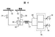
- 真空容器内部に配置されその内側でプラズマが形成される処理室と、この処理室内に配
置され前記プラズマを用いて処理される試料がその上に載せられる試料台と、この試料台
上面を構成してその上に前記試料が載せられる誘電体製の膜内に配置され当該試料を吸着
するための電力が供給されて異なる極性が形成される膜状の2つの電極と、当該2つの電
極と各々の電源との間の給電路上に配置され前記2つの電極各々に接続された2つの給電
線路が同じ軸回りに並列に巻かれたコイル状部分と、このコイル状部分と前記2つの電極
との間において前記2つの給電線路を接続しコンデンサを備えたバイパス線路とを備えた
プラズマ処理装置。 - 請求項1記載のプラズマ処理装置であって、
前記処理室内に前記プラズマを形成する電界を形成する高周波電力を供給する高周波電
源を有し、前記高周波電力の周波数が30乃至300MHzの範囲内であるプラズマ処理
装置。 - 請求項1または2に記載のプラズマ処理装置であって、
前記コイル状部分が内部に芯を有さないプラズマ処理装置。 - 請求項2記載のプラズマ処理装置であって、
前記コイル状部分が前記2つの給電線路上であって当該2つの給電線路の前記2つの電
極からの距離が前記高周波電力の電流の1波長以内に配置されたプラズマ処理装置。 - 請求項2または4に記載のプラズマ処理装置であって、
前記2つの給電線路上の前記コイル状部分と前記各々の電源との間に配置され前記高周
波電力を濾過するフィルタを備えたプラズマ処理装置。
Applications Claiming Priority (1)
| Application Number | Priority Date | Filing Date | Title |
|---|---|---|---|
| PCT/JP2017/011093 WO2018173095A1 (ja) | 2017-03-21 | 2017-03-21 | プラズマ処理装置 |
Publications (2)
| Publication Number | Publication Date |
|---|---|
| JPWO2018173095A1 JPWO2018173095A1 (ja) | 2019-04-04 |
| JP6530859B2 true JP6530859B2 (ja) | 2019-06-12 |
Family
ID=63584322
Family Applications (1)
| Application Number | Title | Priority Date | Filing Date |
|---|---|---|---|
| JP2018511164A Active JP6530859B2 (ja) | 2017-03-21 | 2017-03-21 | プラズマ処理装置 |
Country Status (5)
| Country | Link |
|---|---|
| US (1) | US10825657B2 (ja) |
| JP (1) | JP6530859B2 (ja) |
| KR (1) | KR102056724B1 (ja) |
| TW (1) | TWI701706B (ja) |
| WO (1) | WO2018173095A1 (ja) |
Families Citing this family (7)
| Publication number | Priority date | Publication date | Assignee | Title |
|---|---|---|---|---|
| CN111199860A (zh) * | 2018-11-20 | 2020-05-26 | 江苏鲁汶仪器有限公司 | 一种刻蚀均匀性调节装置及方法 |
| KR102593142B1 (ko) * | 2020-05-19 | 2023-10-25 | 세메스 주식회사 | 기판 처리 장치 및 그의 페라이트 코어 온도 제어 방법 |
| KR102785926B1 (ko) * | 2020-11-06 | 2025-03-26 | 세메스 주식회사 | 기판 처리 장치 |
| JP7534235B2 (ja) * | 2021-02-01 | 2024-08-14 | 東京エレクトロン株式会社 | フィルタ回路及びプラズマ処理装置 |
| JP7645732B2 (ja) * | 2021-07-16 | 2025-03-14 | 東京エレクトロン株式会社 | プラズマ処理装置及び処理方法 |
| CN116344307A (zh) * | 2021-12-24 | 2023-06-27 | 中微半导体设备(上海)股份有限公司 | 静电卡盘系统及半导体处理设备 |
| US12573588B2 (en) | 2024-04-02 | 2026-03-10 | Applied Materials, Inc. | Plasma processing system configured to deliver a pulsed voltage waveform |
Family Cites Families (9)
| Publication number | Priority date | Publication date | Assignee | Title |
|---|---|---|---|---|
| JPS605539A (ja) | 1983-06-23 | 1985-01-12 | Fujitsu Ltd | プラズマ処理方法 |
| JP2685610B2 (ja) | 1989-12-07 | 1997-12-03 | 東京エレクトロン株式会社 | プラズマ処理装置 |
| JP3306677B2 (ja) * | 1993-05-12 | 2002-07-24 | 東京エレクトロン株式会社 | 自己バイアス測定方法及び装置並びに静電吸着装置 |
| US5557215A (en) * | 1993-05-12 | 1996-09-17 | Tokyo Electron Limited | Self-bias measuring method, apparatus thereof and electrostatic chucking apparatus |
| JP6027374B2 (ja) | 2012-09-12 | 2016-11-16 | 東京エレクトロン株式会社 | プラズマ処理装置及びフィルタユニット |
| JP2016031955A (ja) | 2014-07-28 | 2016-03-07 | 株式会社日立ハイテクノロジーズ | プラズマ処理装置およびプラズマ処理方法 |
| US9779919B2 (en) * | 2015-01-09 | 2017-10-03 | Hitachi High-Technologies Corporation | Plasma processing apparatus and plasma processing method |
| JP6567943B2 (ja) | 2015-01-09 | 2019-08-28 | 株式会社日立ハイテクノロジーズ | プラズマ処理装置およびプラズマ処理方法 |
| JP6650593B2 (ja) * | 2017-02-17 | 2020-02-19 | パナソニックIpマネジメント株式会社 | プラズマ処理装置およびプラズマ処理方法 |
-
2017
- 2017-03-21 KR KR1020187003988A patent/KR102056724B1/ko active Active
- 2017-03-21 JP JP2018511164A patent/JP6530859B2/ja active Active
- 2017-03-21 US US15/755,338 patent/US10825657B2/en active Active
- 2017-03-21 WO PCT/JP2017/011093 patent/WO2018173095A1/ja not_active Ceased
-
2018
- 2018-02-26 TW TW107106355A patent/TWI701706B/zh active
Also Published As
| Publication number | Publication date |
|---|---|
| WO2018173095A1 (ja) | 2018-09-27 |
| TWI701706B (zh) | 2020-08-11 |
| KR20180125432A (ko) | 2018-11-23 |
| KR102056724B1 (ko) | 2019-12-17 |
| US10825657B2 (en) | 2020-11-03 |
| TW201843695A (zh) | 2018-12-16 |
| JPWO2018173095A1 (ja) | 2019-04-04 |
| US20200234924A1 (en) | 2020-07-23 |
Similar Documents
| Publication | Publication Date | Title |
|---|---|---|
| JP6530859B2 (ja) | プラズマ処理装置 | |
| JP5800547B2 (ja) | プラズマ処理装置及びプラズマ処理方法 | |
| KR101873485B1 (ko) | 플라즈마 처리 장치 | |
| US9530619B2 (en) | Plasma processing apparatus and filter unit | |
| US6265031B1 (en) | Method for plasma processing by shaping an induced electric field | |
| JP6027374B2 (ja) | プラズマ処理装置及びフィルタユニット | |
| JP5723130B2 (ja) | プラズマ処理装置 | |
| JP5309179B2 (ja) | 均一なプロセス速度を生成するためのプラズマ処理装置及び結合窓構成 | |
| CN104994676B (zh) | 等离子体处理装置 | |
| US9218943B2 (en) | Plasma processing apparatus and plasma processing method | |
| US20150243486A1 (en) | Plasma processing apparatus | |
| US6850012B2 (en) | Plasma processing apparatus | |
| JP2011135052A (ja) | プラズマ処理装置 | |
| TW201814407A (zh) | 具有流通源的腔室 | |
| CN101506950A (zh) | 使用多频率rf功率的混合rf电容和电感耦合等离子源及其使用方法 | |
| US9754766B2 (en) | Plasma processing apparatus | |
| JP6062461B2 (ja) | プラズマ処理装置 | |
| TW202004831A (zh) | 電漿處理裝置 | |
| JP6097317B2 (ja) | プラズマ処理方法 | |
| WO2020121588A1 (ja) | プラズマ処理装置 | |
| JP2016046357A (ja) | プラズマ処理装置 | |
| KR20240178772A (ko) | 유도 결합형 플라즈마 안테나 및 이를 포함하는 기판 처리 장치 |
Legal Events
| Date | Code | Title | Description |
|---|---|---|---|
| A521 | Request for written amendment filed |
Free format text: JAPANESE INTERMEDIATE CODE: A523 Effective date: 20180227 |
|
| A621 | Written request for application examination |
Free format text: JAPANESE INTERMEDIATE CODE: A621 Effective date: 20180227 |
|
| A131 | Notification of reasons for refusal |
Free format text: JAPANESE INTERMEDIATE CODE: A131 Effective date: 20181106 |
|
| A521 | Request for written amendment filed |
Free format text: JAPANESE INTERMEDIATE CODE: A523 Effective date: 20181227 |
|
| TRDD | Decision of grant or rejection written | ||
| A01 | Written decision to grant a patent or to grant a registration (utility model) |
Free format text: JAPANESE INTERMEDIATE CODE: A01 Effective date: 20190423 |
|
| A61 | First payment of annual fees (during grant procedure) |
Free format text: JAPANESE INTERMEDIATE CODE: A61 Effective date: 20190517 |
|
| R150 | Certificate of patent or registration of utility model |
Ref document number: 6530859 Country of ref document: JP Free format text: JAPANESE INTERMEDIATE CODE: R150 |
|
| S531 | Written request for registration of change of domicile |
Free format text: JAPANESE INTERMEDIATE CODE: R313531 |
|
| S533 | Written request for registration of change of name |
Free format text: JAPANESE INTERMEDIATE CODE: R313533 |
|
| R350 | Written notification of registration of transfer |
Free format text: JAPANESE INTERMEDIATE CODE: R350 |