JP6577662B2 - 配線体、配線基板、及びタッチセンサ - Google Patents
配線体、配線基板、及びタッチセンサ Download PDFInfo
- Publication number
- JP6577662B2 JP6577662B2 JP2018509439A JP2018509439A JP6577662B2 JP 6577662 B2 JP6577662 B2 JP 6577662B2 JP 2018509439 A JP2018509439 A JP 2018509439A JP 2018509439 A JP2018509439 A JP 2018509439A JP 6577662 B2 JP6577662 B2 JP 6577662B2
- Authority
- JP
- Japan
- Prior art keywords
- conductor portion
- conductor
- resin
- wiring body
- face
- Prior art date
- Legal status (The legal status is an assumption and is not a legal conclusion. Google has not performed a legal analysis and makes no representation as to the accuracy of the status listed.)
- Expired - Fee Related
Links
Images

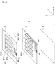


Classifications
-
- G—PHYSICS
- G06—COMPUTING OR CALCULATING; COUNTING
- G06F—ELECTRIC DIGITAL DATA PROCESSING
- G06F3/00—Input arrangements for transferring data to be processed into a form capable of being handled by the computer; Output arrangements for transferring data from processing unit to output unit, e.g. interface arrangements
- G06F3/01—Input arrangements or combined input and output arrangements for interaction between user and computer
- G06F3/03—Arrangements for converting the position or the displacement of a member into a coded form
- G06F3/041—Digitisers, e.g. for touch screens or touch pads, characterised by the transducing means
- G06F3/044—Digitisers, e.g. for touch screens or touch pads, characterised by the transducing means by capacitive means
- G06F3/0445—Digitisers, e.g. for touch screens or touch pads, characterised by the transducing means by capacitive means using two or more layers of sensing electrodes, e.g. using two layers of electrodes separated by a dielectric layer
-
- G—PHYSICS
- G06—COMPUTING OR CALCULATING; COUNTING
- G06F—ELECTRIC DIGITAL DATA PROCESSING
- G06F3/00—Input arrangements for transferring data to be processed into a form capable of being handled by the computer; Output arrangements for transferring data from processing unit to output unit, e.g. interface arrangements
- G06F3/01—Input arrangements or combined input and output arrangements for interaction between user and computer
- G06F3/03—Arrangements for converting the position or the displacement of a member into a coded form
- G06F3/041—Digitisers, e.g. for touch screens or touch pads, characterised by the transducing means
- G06F3/044—Digitisers, e.g. for touch screens or touch pads, characterised by the transducing means by capacitive means
- G06F3/0446—Digitisers, e.g. for touch screens or touch pads, characterised by the transducing means by capacitive means using a grid-like structure of electrodes in at least two directions, e.g. using row and column electrodes
-
- G—PHYSICS
- G06—COMPUTING OR CALCULATING; COUNTING
- G06F—ELECTRIC DIGITAL DATA PROCESSING
- G06F2203/00—Indexing scheme relating to G06F3/00 - G06F3/048
- G06F2203/041—Indexing scheme relating to G06F3/041 - G06F3/045
- G06F2203/04103—Manufacturing, i.e. details related to manufacturing processes specially suited for touch sensitive devices
-
- G—PHYSICS
- G06—COMPUTING OR CALCULATING; COUNTING
- G06F—ELECTRIC DIGITAL DATA PROCESSING
- G06F2203/00—Indexing scheme relating to G06F3/00 - G06F3/048
- G06F2203/041—Indexing scheme relating to G06F3/041 - G06F3/045
- G06F2203/04112—Electrode mesh in capacitive digitiser: electrode for touch sensing is formed of a mesh of very fine, normally metallic, interconnected lines that are almost invisible to see. This provides a quite large but transparent electrode surface, without need for ITO or similar transparent conductive material
Landscapes
- Engineering & Computer Science (AREA)
- General Engineering & Computer Science (AREA)
- Theoretical Computer Science (AREA)
- Human Computer Interaction (AREA)
- Physics & Mathematics (AREA)
- General Physics & Mathematics (AREA)
- Structure Of Printed Boards (AREA)
- Position Input By Displaying (AREA)
Applications Claiming Priority (3)
| Application Number | Priority Date | Filing Date | Title |
|---|---|---|---|
| JP2016067614 | 2016-03-30 | ||
| JP2016067614 | 2016-03-30 | ||
| PCT/JP2017/013269 WO2017170870A1 (ja) | 2016-03-30 | 2017-03-30 | 配線体、配線基板、及びタッチセンサ |
Publications (2)
| Publication Number | Publication Date |
|---|---|
| JPWO2017170870A1 JPWO2017170870A1 (ja) | 2018-08-09 |
| JP6577662B2 true JP6577662B2 (ja) | 2019-09-18 |
Family
ID=59965856
Family Applications (1)
| Application Number | Title | Priority Date | Filing Date |
|---|---|---|---|
| JP2018509439A Expired - Fee Related JP6577662B2 (ja) | 2016-03-30 | 2017-03-30 | 配線体、配線基板、及びタッチセンサ |
Country Status (6)
| Country | Link |
|---|---|
| US (1) | US20200310584A1 (de) |
| EP (1) | EP3438800A4 (de) |
| JP (1) | JP6577662B2 (de) |
| CN (1) | CN108700965A (de) |
| TW (1) | TWI649767B (de) |
| WO (1) | WO2017170870A1 (de) |
Families Citing this family (3)
| Publication number | Priority date | Publication date | Assignee | Title |
|---|---|---|---|---|
| WO2020169188A1 (en) * | 2019-02-20 | 2020-08-27 | Scrona Ag | Optically transparent conductor assembly with electrical tracks and touch sensor comprising the same |
| JP7622987B2 (ja) * | 2019-03-28 | 2025-01-28 | 京東方科技集團股▲ふん▼有限公司 | タッチ基板、タッチ装置及びタッチ検出方法 |
| KR20250027329A (ko) * | 2023-08-16 | 2025-02-26 | 삼성디스플레이 주식회사 | 표시 장치 |
Family Cites Families (20)
| Publication number | Priority date | Publication date | Assignee | Title |
|---|---|---|---|---|
| JP2004193168A (ja) * | 2002-12-06 | 2004-07-08 | Kyocera Corp | 配線基板およびその製造方法 |
| JP5591834B2 (ja) * | 2009-03-04 | 2014-09-17 | ナム、ドンシク | タッチパネルセンサー |
| JP2011175412A (ja) * | 2010-02-24 | 2011-09-08 | Shin Etsu Polymer Co Ltd | 静電容量式のタッチパネルスイッチ |
| JP2012169353A (ja) * | 2011-02-10 | 2012-09-06 | Dainippon Printing Co Ltd | 光学シート、及びそのシートを用いたプラズマディスプレイ用前面フィルタ |
| JP5224203B1 (ja) * | 2012-07-11 | 2013-07-03 | 大日本印刷株式会社 | タッチパネルセンサ、タッチパネル装置および表示装置 |
| JP6098787B2 (ja) * | 2012-09-25 | 2017-03-22 | グンゼ株式会社 | タッチパネル付き表示装置 |
| JP5922008B2 (ja) * | 2012-11-30 | 2016-05-24 | 富士フイルム株式会社 | 転写フィルムおよび透明積層体、それらの製造方法、静電容量型入力装置ならびに画像表示装置 |
| KR101588924B1 (ko) * | 2012-12-24 | 2016-01-26 | 삼성전기주식회사 | 터치센서 |
| JP6014687B2 (ja) * | 2013-01-29 | 2016-10-25 | シャープ株式会社 | 入力装置及びその製造方法、並びに電子情報機器 |
| US9594454B2 (en) * | 2013-03-29 | 2017-03-14 | Sharp Kabushiki Kaisha | Touch-panel substrate and electronic device |
| JP5686445B2 (ja) * | 2013-07-01 | 2015-03-18 | 日本写真印刷株式会社 | 相互静電容量方式タッチパネル |
| JP5969961B2 (ja) * | 2013-07-12 | 2016-08-17 | 富士フイルム株式会社 | 配線基板 |
| TW201535173A (zh) * | 2014-03-04 | 2015-09-16 | Wintek Corp | 裝飾面板及觸控裝置 |
| WO2015146277A1 (ja) * | 2014-03-28 | 2015-10-01 | 株式会社カネカ | タッチパネル、表示装置、並びに、タッチパネルの製造方法 |
| JP2015195004A (ja) * | 2014-03-28 | 2015-11-05 | 富士フイルム株式会社 | 導電性フィルム及びタッチパネルモジュール |
| JP6200582B2 (ja) * | 2014-04-08 | 2017-09-20 | 株式会社フジクラ | 配線体及び配線基板 |
| CN104076982B (zh) * | 2014-06-24 | 2017-01-18 | 京东方科技集团股份有限公司 | 一种触摸屏及其制作方法、显示装置 |
| CN204288188U (zh) * | 2014-12-23 | 2015-04-22 | 江苏吉创光电有限公司 | 一种抗眩式新型电容式触控面板结构 |
| JP6483801B2 (ja) * | 2015-02-27 | 2019-03-13 | 株式会社フジクラ | タッチセンサ |
| CN105404418B (zh) * | 2015-11-03 | 2018-09-04 | 京东方科技集团股份有限公司 | 触控屏及其制备方法、显示面板和显示装置 |
-
2017
- 2017-03-30 CN CN201780011145.3A patent/CN108700965A/zh not_active Withdrawn
- 2017-03-30 TW TW106110746A patent/TWI649767B/zh not_active IP Right Cessation
- 2017-03-30 US US16/089,983 patent/US20200310584A1/en not_active Abandoned
- 2017-03-30 EP EP17775404.1A patent/EP3438800A4/de not_active Withdrawn
- 2017-03-30 WO PCT/JP2017/013269 patent/WO2017170870A1/ja not_active Ceased
- 2017-03-30 JP JP2018509439A patent/JP6577662B2/ja not_active Expired - Fee Related
Also Published As
| Publication number | Publication date |
|---|---|
| EP3438800A1 (de) | 2019-02-06 |
| US20200310584A1 (en) | 2020-10-01 |
| CN108700965A (zh) | 2018-10-23 |
| WO2017170870A1 (ja) | 2017-10-05 |
| EP3438800A4 (de) | 2019-10-23 |
| TWI649767B (zh) | 2019-02-01 |
| JPWO2017170870A1 (ja) | 2018-08-09 |
| TW201804481A (zh) | 2018-02-01 |
Similar Documents
| Publication | Publication Date | Title |
|---|---|---|
| JP6735212B2 (ja) | 配線体、配線基板、タッチセンサ、及び配線体の製造方法 | |
| JP6159904B2 (ja) | 配線体、配線基板、及びタッチセンサ | |
| US20190018524A1 (en) | Wiring body, wiring board, and touch sensor | |
| WO2016208636A1 (ja) | 配線体、配線基板、及びタッチセンサ | |
| JPWO2016136965A1 (ja) | 配線体、配線基板、及びタッチセンサ | |
| JP6027296B1 (ja) | 配線体、配線基板、及びタッチセンサ | |
| JP6140383B2 (ja) | 導体層付き構造体の製造方法、基材付き配線体、基材付き構造体、及びタッチセンサ | |
| JPWO2017187266A1 (ja) | 配線体、配線体アセンブリ、配線基板、及びタッチセンサ | |
| JP6483801B2 (ja) | タッチセンサ | |
| JPWO2016136971A1 (ja) | タッチセンサ用配線体、タッチセンサ用配線基板及びタッチセンサ | |
| JP6577662B2 (ja) | 配線体、配線基板、及びタッチセンサ | |
| JP6483245B2 (ja) | 配線体、配線基板、タッチセンサ、及び配線体の製造方法 | |
| TWI652698B (zh) | 導線體、導線基板及觸控感測器 | |
| JP6143909B1 (ja) | 配線体、配線基板、タッチセンサ、及び配線体の製造方法 | |
| JP2018060411A (ja) | 配線体、配線基板、及びタッチセンサ | |
| JP6317038B2 (ja) | 配線体、配線基板、及びタッチセンサ |
Legal Events
| Date | Code | Title | Description |
|---|---|---|---|
| A621 | Written request for application examination |
Free format text: JAPANESE INTERMEDIATE CODE: A621 Effective date: 20180424 |
|
| A131 | Notification of reasons for refusal |
Free format text: JAPANESE INTERMEDIATE CODE: A131 Effective date: 20190611 |
|
| A521 | Request for written amendment filed |
Free format text: JAPANESE INTERMEDIATE CODE: A523 Effective date: 20190805 |
|
| TRDD | Decision of grant or rejection written | ||
| A01 | Written decision to grant a patent or to grant a registration (utility model) |
Free format text: JAPANESE INTERMEDIATE CODE: A01 Effective date: 20190820 |
|
| A61 | First payment of annual fees (during grant procedure) |
Free format text: JAPANESE INTERMEDIATE CODE: A61 Effective date: 20190822 |
|
| R151 | Written notification of patent or utility model registration |
Ref document number: 6577662 Country of ref document: JP Free format text: JAPANESE INTERMEDIATE CODE: R151 |
|
| LAPS | Cancellation because of no payment of annual fees |