JP6589662B2 - 半導体積層体および受光素子 - Google Patents
半導体積層体および受光素子 Download PDFInfo
- Publication number
- JP6589662B2 JP6589662B2 JP2016013120A JP2016013120A JP6589662B2 JP 6589662 B2 JP6589662 B2 JP 6589662B2 JP 2016013120 A JP2016013120 A JP 2016013120A JP 2016013120 A JP2016013120 A JP 2016013120A JP 6589662 B2 JP6589662 B2 JP 6589662B2
- Authority
- JP
- Japan
- Prior art keywords
- semiconductor layer
- semiconductor
- layer
- quantum well
- light receiving
- Prior art date
- Legal status (The legal status is an assumption and is not a legal conclusion. Google has not performed a legal analysis and makes no representation as to the accuracy of the status listed.)
- Active
Links
Images




Classifications
-
- H—ELECTRICITY
- H10—SEMICONDUCTOR DEVICES; ELECTRIC SOLID-STATE DEVICES NOT OTHERWISE PROVIDED FOR
- H10F—INORGANIC SEMICONDUCTOR DEVICES SENSITIVE TO INFRARED RADIATION, LIGHT, ELECTROMAGNETIC RADIATION OF SHORTER WAVELENGTH OR CORPUSCULAR RADIATION
- H10F77/00—Constructional details of devices covered by this subclass
- H10F77/10—Semiconductor bodies
- H10F77/12—Active materials
- H10F77/124—Active materials comprising only Group III-V materials, e.g. GaAs
- H10F77/1243—Active materials comprising only Group III-V materials, e.g. GaAs characterised by the dopants
-
- H—ELECTRICITY
- H10—SEMICONDUCTOR DEVICES; ELECTRIC SOLID-STATE DEVICES NOT OTHERWISE PROVIDED FOR
- H10F—INORGANIC SEMICONDUCTOR DEVICES SENSITIVE TO INFRARED RADIATION, LIGHT, ELECTROMAGNETIC RADIATION OF SHORTER WAVELENGTH OR CORPUSCULAR RADIATION
- H10F30/00—Individual radiation-sensitive semiconductor devices in which radiation controls the flow of current through the devices, e.g. photodetectors
- H10F30/20—Individual radiation-sensitive semiconductor devices in which radiation controls the flow of current through the devices, e.g. photodetectors the devices having potential barriers, e.g. phototransistors
- H10F30/21—Individual radiation-sensitive semiconductor devices in which radiation controls the flow of current through the devices, e.g. photodetectors the devices having potential barriers, e.g. phototransistors the devices being sensitive to infrared, visible or ultraviolet radiation
-
- H—ELECTRICITY
- H10—SEMICONDUCTOR DEVICES; ELECTRIC SOLID-STATE DEVICES NOT OTHERWISE PROVIDED FOR
- H10F—INORGANIC SEMICONDUCTOR DEVICES SENSITIVE TO INFRARED RADIATION, LIGHT, ELECTROMAGNETIC RADIATION OF SHORTER WAVELENGTH OR CORPUSCULAR RADIATION
- H10F30/00—Individual radiation-sensitive semiconductor devices in which radiation controls the flow of current through the devices, e.g. photodetectors
- H10F30/20—Individual radiation-sensitive semiconductor devices in which radiation controls the flow of current through the devices, e.g. photodetectors the devices having potential barriers, e.g. phototransistors
- H10F30/21—Individual radiation-sensitive semiconductor devices in which radiation controls the flow of current through the devices, e.g. photodetectors the devices having potential barriers, e.g. phototransistors the devices being sensitive to infrared, visible or ultraviolet radiation
- H10F30/22—Individual radiation-sensitive semiconductor devices in which radiation controls the flow of current through the devices, e.g. photodetectors the devices having potential barriers, e.g. phototransistors the devices being sensitive to infrared, visible or ultraviolet radiation the devices having only one potential barrier, e.g. photodiodes
- H10F30/222—Individual radiation-sensitive semiconductor devices in which radiation controls the flow of current through the devices, e.g. photodetectors the devices having potential barriers, e.g. phototransistors the devices being sensitive to infrared, visible or ultraviolet radiation the devices having only one potential barrier, e.g. photodiodes the potential barrier being a PN heterojunction
-
- H—ELECTRICITY
- H10—SEMICONDUCTOR DEVICES; ELECTRIC SOLID-STATE DEVICES NOT OTHERWISE PROVIDED FOR
- H10F—INORGANIC SEMICONDUCTOR DEVICES SENSITIVE TO INFRARED RADIATION, LIGHT, ELECTROMAGNETIC RADIATION OF SHORTER WAVELENGTH OR CORPUSCULAR RADIATION
- H10F30/00—Individual radiation-sensitive semiconductor devices in which radiation controls the flow of current through the devices, e.g. photodetectors
- H10F30/20—Individual radiation-sensitive semiconductor devices in which radiation controls the flow of current through the devices, e.g. photodetectors the devices having potential barriers, e.g. phototransistors
- H10F30/21—Individual radiation-sensitive semiconductor devices in which radiation controls the flow of current through the devices, e.g. photodetectors the devices having potential barriers, e.g. phototransistors the devices being sensitive to infrared, visible or ultraviolet radiation
- H10F30/22—Individual radiation-sensitive semiconductor devices in which radiation controls the flow of current through the devices, e.g. photodetectors the devices having potential barriers, e.g. phototransistors the devices being sensitive to infrared, visible or ultraviolet radiation the devices having only one potential barrier, e.g. photodiodes
- H10F30/223—Individual radiation-sensitive semiconductor devices in which radiation controls the flow of current through the devices, e.g. photodetectors the devices having potential barriers, e.g. phototransistors the devices being sensitive to infrared, visible or ultraviolet radiation the devices having only one potential barrier, e.g. photodiodes the potential barrier being a PIN barrier
-
- H—ELECTRICITY
- H10—SEMICONDUCTOR DEVICES; ELECTRIC SOLID-STATE DEVICES NOT OTHERWISE PROVIDED FOR
- H10F—INORGANIC SEMICONDUCTOR DEVICES SENSITIVE TO INFRARED RADIATION, LIGHT, ELECTROMAGNETIC RADIATION OF SHORTER WAVELENGTH OR CORPUSCULAR RADIATION
- H10F39/00—Integrated devices, or assemblies of multiple devices, comprising at least one element covered by group H10F30/00, e.g. radiation detectors comprising photodiode arrays
- H10F39/10—Integrated devices
- H10F39/12—Image sensors
- H10F39/18—Complementary metal-oxide-semiconductor [CMOS] image sensors; Photodiode array image sensors
- H10F39/184—Infrared image sensors
- H10F39/1847—Multispectral infrared image sensors having a stacked structure, e.g. NPN, NPNPN or multiple quantum well [MQW] structures
-
- H—ELECTRICITY
- H10—SEMICONDUCTOR DEVICES; ELECTRIC SOLID-STATE DEVICES NOT OTHERWISE PROVIDED FOR
- H10F—INORGANIC SEMICONDUCTOR DEVICES SENSITIVE TO INFRARED RADIATION, LIGHT, ELECTROMAGNETIC RADIATION OF SHORTER WAVELENGTH OR CORPUSCULAR RADIATION
- H10F71/00—Manufacture or treatment of devices covered by this subclass
- H10F71/127—The active layers comprising only Group III-V materials, e.g. GaAs or InP
- H10F71/1272—The active layers comprising only Group III-V materials, e.g. GaAs or InP comprising at least three elements, e.g. GaAlAs or InGaAsP
-
- H—ELECTRICITY
- H10—SEMICONDUCTOR DEVICES; ELECTRIC SOLID-STATE DEVICES NOT OTHERWISE PROVIDED FOR
- H10F—INORGANIC SEMICONDUCTOR DEVICES SENSITIVE TO INFRARED RADIATION, LIGHT, ELECTROMAGNETIC RADIATION OF SHORTER WAVELENGTH OR CORPUSCULAR RADIATION
- H10F77/00—Constructional details of devices covered by this subclass
- H10F77/10—Semiconductor bodies
- H10F77/12—Active materials
- H10F77/124—Active materials comprising only Group III-V materials, e.g. GaAs
- H10F77/1248—Active materials comprising only Group III-V materials, e.g. GaAs having three or more elements, e.g. GaAlAs, InGaAs or InGaAsP
-
- H—ELECTRICITY
- H10—SEMICONDUCTOR DEVICES; ELECTRIC SOLID-STATE DEVICES NOT OTHERWISE PROVIDED FOR
- H10F—INORGANIC SEMICONDUCTOR DEVICES SENSITIVE TO INFRARED RADIATION, LIGHT, ELECTROMAGNETIC RADIATION OF SHORTER WAVELENGTH OR CORPUSCULAR RADIATION
- H10F77/00—Constructional details of devices covered by this subclass
- H10F77/10—Semiconductor bodies
- H10F77/12—Active materials
- H10F77/124—Active materials comprising only Group III-V materials, e.g. GaAs
- H10F77/1248—Active materials comprising only Group III-V materials, e.g. GaAs having three or more elements, e.g. GaAlAs, InGaAs or InGaAsP
- H10F77/12485—Active materials comprising only Group III-V materials, e.g. GaAs having three or more elements, e.g. GaAlAs, InGaAs or InGaAsP comprising nitride compounds, e.g. InGaN
-
- H—ELECTRICITY
- H10—SEMICONDUCTOR DEVICES; ELECTRIC SOLID-STATE DEVICES NOT OTHERWISE PROVIDED FOR
- H10F—INORGANIC SEMICONDUCTOR DEVICES SENSITIVE TO INFRARED RADIATION, LIGHT, ELECTROMAGNETIC RADIATION OF SHORTER WAVELENGTH OR CORPUSCULAR RADIATION
- H10F77/00—Constructional details of devices covered by this subclass
- H10F77/10—Semiconductor bodies
- H10F77/14—Shape of semiconductor bodies; Shapes, relative sizes or dispositions of semiconductor regions within semiconductor bodies
-
- H—ELECTRICITY
- H10—SEMICONDUCTOR DEVICES; ELECTRIC SOLID-STATE DEVICES NOT OTHERWISE PROVIDED FOR
- H10F—INORGANIC SEMICONDUCTOR DEVICES SENSITIVE TO INFRARED RADIATION, LIGHT, ELECTROMAGNETIC RADIATION OF SHORTER WAVELENGTH OR CORPUSCULAR RADIATION
- H10F77/00—Constructional details of devices covered by this subclass
- H10F77/10—Semiconductor bodies
- H10F77/14—Shape of semiconductor bodies; Shapes, relative sizes or dispositions of semiconductor regions within semiconductor bodies
- H10F77/143—Shape of semiconductor bodies; Shapes, relative sizes or dispositions of semiconductor regions within semiconductor bodies comprising quantum structures
-
- H—ELECTRICITY
- H10—SEMICONDUCTOR DEVICES; ELECTRIC SOLID-STATE DEVICES NOT OTHERWISE PROVIDED FOR
- H10F—INORGANIC SEMICONDUCTOR DEVICES SENSITIVE TO INFRARED RADIATION, LIGHT, ELECTROMAGNETIC RADIATION OF SHORTER WAVELENGTH OR CORPUSCULAR RADIATION
- H10F77/00—Constructional details of devices covered by this subclass
- H10F77/10—Semiconductor bodies
- H10F77/14—Shape of semiconductor bodies; Shapes, relative sizes or dispositions of semiconductor regions within semiconductor bodies
- H10F77/146—Superlattices; Multiple quantum well structures
-
- H—ELECTRICITY
- H10—SEMICONDUCTOR DEVICES; ELECTRIC SOLID-STATE DEVICES NOT OTHERWISE PROVIDED FOR
- H10F—INORGANIC SEMICONDUCTOR DEVICES SENSITIVE TO INFRARED RADIATION, LIGHT, ELECTROMAGNETIC RADIATION OF SHORTER WAVELENGTH OR CORPUSCULAR RADIATION
- H10F77/00—Constructional details of devices covered by this subclass
- H10F77/30—Coatings
- H10F77/306—Coatings for devices having potential barriers
Landscapes
- Light Receiving Elements (AREA)
- Physics & Mathematics (AREA)
- Spectroscopy & Molecular Physics (AREA)
Description
最初に本願発明の実施態様を列記して説明する。本願の半導体積層体は、III−V族化合物半導体からなり、導電型が第1導電型である第1半導体層と、III−V族化合物半導体からなる量子井戸受光層と、III−V族化合物半導体からなる第2半導体層と、III−V族化合物半導体からなる第3半導体層と、III−V族化合物半導体からなり、導電型が第1導電型とは異なる第2導電型である第4半導体層と、を備える。第1半導体層、量子井戸受光層、第2半導体層、第3半導体層および第4半導体層は、この順に積層される。第2導電型のキャリアを生成する不純物の濃度は、第4半導体層よりも第3半導体層において低い。第2半導体層において多数キャリアを生成する不純物の濃度は、第2半導体層よりも第3半導体層において低い。
次に、本発明にかかる半導体積層体の実施の形態を、以下に図面を参照しつつ説明する。なお、以下の図面において同一または相当する部分には同一の参照番号を付しその説明は繰返さない。
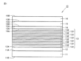
図1を参照して、実施の形態1における半導体積層体10は、基板11と、第1半導体層12と、量子井戸受光層としての量子井戸構造13と、第2半導体層14と、第3半導体層15と、第4半導体層16とを備えている。
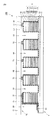
次に、本発明にかかる受光素子の他の実施の形態である実施の形態2における受光素子およびセンサについて説明する。図9および図2を参照して、実施の形態2の赤外線受光素子1は、図2に示す構造を単位構造とし、当該単位構造が、基板11の一方の主面11Aが延在する方向に複数繰り返される構造を有している。そして、赤外線受光素子1は、画素に対応する複数のp側電極92を有する。一方、n側電極91は1つだけ配置される。

10 半導体積層体
11 基板
11A 主面
12 第1半導体層
12A 第1主面
13 量子井戸構造
131 第1要素層
132 第2要素層
13A 主面
14 第2半導体層
14A 主面
14B 主面
15 第3半導体層
15A 主面
15B 主面
16 第4半導体層
16B 主面
70 読み出し回路
71 本体
72,73 バンプ
75 配線
80 パッシベーション膜
81,82 開口部
91 n側電極
92 p側電極
99 トレンチ
99A 側壁
99B 底壁
100 赤外線センサ
Claims (11)
- III−V族化合物半導体からなり、導電型が第1導電型である第1半導体層と、
III−V族化合物半導体からなる量子井戸受光層と、
III−V族化合物半導体からなる第2半導体層と、
III−V族化合物半導体からなる第3半導体層と、
III−V族化合物半導体からなり、導電型が前記第1導電型とは異なる第2導電型である第4半導体層と、を備え、
前記第1半導体層、前記量子井戸受光層、前記第2半導体層、前記第3半導体層および前記第4半導体層は、この順に積層され、
前記第2導電型のキャリアを生成する不純物の濃度は、前記第4半導体層よりも前記第3半導体層において低く、
前記第2半導体層において多数キャリアを生成する不純物の濃度は、前記第2半導体層よりも前記第3半導体層において低く、
前記第2半導体層における多数キャリアを生成する不純物の濃度は5×10 14 cm −3 以上5×10 18 cm −3 以下であり、
前記第2半導体層の厚みは500nm以下である、半導体積層体。 - 前記第3半導体層における前記第1導電型のキャリアを生成する不純物の濃度および前記第2導電型のキャリアを生成する不純物の濃度は、いずれも5×1014cm−3未満である、請求項1に記載の半導体積層体。
- 前記第2半導体層において多数キャリアを生成する不純物の濃度は、前記第4半導体層における前記第2導電型のキャリアを生成する不純物の濃度よりも低い、請求項1または2に記載の半導体積層体。
- 前記第2半導体層の厚みは、前記第3半導体層の厚みよりも小さい、請求項1から請求項3のいずれか1項に記載の半導体積層体。
- 前記第2半導体層において多数キャリアを生成する不純物は、Si、S、Se、Ge、TeおよびSnからなる群から選択される一種以上、またはZn、Be、MgおよびCからなる群から選択される一種以上である、請求項1から請求項4のいずれか1項に記載の半導体積層体。
- 前記量子井戸受光層は、InxGa1−xAs(xは0.38以上1以下)層とGaAs1−ySby(yは0.36以上1以下)層とのペア、またはGa1−uInuNvAs1−v(uは0.4以上0.8以下、vは0を超え0.2以下)層とGaAs1−ySby(yは0.36以上0.62以下)層とのペアを含む多重量子井戸構造である、請求項1から請求項5のいずれか1項に記載の半導体積層体。
- 前記第1半導体層から見て前記量子井戸受光層とは反対側に位置する基板をさらに含み、
前記基板は、GaAs、GaP、GaSb、InP、InAs、InSb、AlSb、またはAlAsからなる、請求項6に記載の半導体積層体。 - 前記第2半導体層は、前記量子井戸受光層を構成する半導体層と同一のIII−V族化合物半導体からなる、請求項1から請求項7のいずれか1項に記載の半導体積層体。
- 前記量子井戸受光層の厚みは1μm以上である、請求項1から請求項8のいずれか1項に記載の半導体積層体。
- 前記第1半導体層と前記量子井戸受光層との界面、前記量子井戸受光層と前記第2半導体層との界面、前記第2半導体層と前記第3半導体層との界面、および前記第3半導体層と前記第4半導体層との界面における、酸素の濃度、炭素の濃度および水素の濃度は、いずれも1×1017cm−3以下である、請求項1から請求項9のいずれか1項に記載の半導体積層体。
- 請求項1から請求項10のいずれか1項に記載の半導体積層体と、
前記半導体積層体上に形成された電極と、を備える、受光素子。
Priority Applications (3)
| Application Number | Priority Date | Filing Date | Title |
|---|---|---|---|
| JP2016013120A JP6589662B2 (ja) | 2016-01-27 | 2016-01-27 | 半導体積層体および受光素子 |
| US16/073,006 US10326034B2 (en) | 2016-01-27 | 2017-01-24 | Semiconductor laminate and light-receiving element |
| PCT/JP2017/002236 WO2017130929A1 (ja) | 2016-01-27 | 2017-01-24 | 半導体積層体および受光素子 |
Applications Claiming Priority (1)
| Application Number | Priority Date | Filing Date | Title |
|---|---|---|---|
| JP2016013120A JP6589662B2 (ja) | 2016-01-27 | 2016-01-27 | 半導体積層体および受光素子 |
Publications (2)
| Publication Number | Publication Date |
|---|---|
| JP2017135228A JP2017135228A (ja) | 2017-08-03 |
| JP6589662B2 true JP6589662B2 (ja) | 2019-10-16 |
Family
ID=59397990
Family Applications (1)
| Application Number | Title | Priority Date | Filing Date |
|---|---|---|---|
| JP2016013120A Active JP6589662B2 (ja) | 2016-01-27 | 2016-01-27 | 半導体積層体および受光素子 |
Country Status (3)
| Country | Link |
|---|---|
| US (1) | US10326034B2 (ja) |
| JP (1) | JP6589662B2 (ja) |
| WO (1) | WO2017130929A1 (ja) |
Families Citing this family (5)
| Publication number | Priority date | Publication date | Assignee | Title |
|---|---|---|---|---|
| US11081605B2 (en) * | 2017-09-01 | 2021-08-03 | Sumitomo Electric Industries, Ltd. | Semiconductor laminate, light-receiving element, and method for manufacturing semiconductor laminate |
| JP6909165B2 (ja) * | 2018-01-15 | 2021-07-28 | 富士通株式会社 | 赤外線検出器、撮像素子、撮像システム、赤外線検出器の製造方法 |
| JP7458696B2 (ja) * | 2018-05-16 | 2024-04-01 | 住友電気工業株式会社 | 半導体積層体および受光素子 |
| TWI803556B (zh) * | 2018-12-28 | 2023-06-01 | 晶元光電股份有限公司 | 半導體疊層、半導體元件及其製造方法 |
| US12278304B2 (en) * | 2021-02-04 | 2025-04-15 | Mellanox Technologies, Ltd. | High modulation speed PIN-type photodiode |
Family Cites Families (10)
| Publication number | Priority date | Publication date | Assignee | Title |
|---|---|---|---|---|
| KR970011140B1 (ko) * | 1993-12-08 | 1997-07-07 | 한국전자통신연구원 | 공명 투과광전 소자의 구조 |
| KR100244524B1 (ko) * | 1997-01-16 | 2000-02-01 | 정선종 | 광제어공명투과다이오드 |
| JP2004109312A (ja) * | 2002-09-17 | 2004-04-08 | Mitsubishi Electric Corp | 導波路型半導体光デバイスおよびその製造方法 |
| US7838869B2 (en) * | 2005-10-21 | 2010-11-23 | Georgia State University Research Foundation, Inc. | Dual band photodetector |
| CN102265411B (zh) * | 2008-12-26 | 2014-06-11 | 住友电气工业株式会社 | 受光元件、受光元件阵列、制造受光元件的方法以及制造受光元件阵列的方法 |
| JP2012174977A (ja) * | 2011-02-23 | 2012-09-10 | Sumitomo Electric Ind Ltd | 受光素子およびその製造方法 |
| JP5512583B2 (ja) * | 2011-03-29 | 2014-06-04 | 旭化成エレクトロニクス株式会社 | 量子型赤外線センサ |
| CN103022218B (zh) * | 2012-12-26 | 2015-10-21 | 华中科技大学 | 一种InAs雪崩光电二极管及其制造方法 |
| JP2015082573A (ja) * | 2013-10-22 | 2015-04-27 | 住友電気工業株式会社 | エピタキシャルウエハおよびその製造方法 |
| JP6233070B2 (ja) * | 2014-02-05 | 2017-11-22 | 住友電気工業株式会社 | 半導体積層体および半導体装置、ならびにそれらの製造方法 |
-
2016
- 2016-01-27 JP JP2016013120A patent/JP6589662B2/ja active Active
-
2017
- 2017-01-24 WO PCT/JP2017/002236 patent/WO2017130929A1/ja not_active Ceased
- 2017-01-24 US US16/073,006 patent/US10326034B2/en active Active
Also Published As
| Publication number | Publication date |
|---|---|
| US10326034B2 (en) | 2019-06-18 |
| JP2017135228A (ja) | 2017-08-03 |
| WO2017130929A1 (ja) | 2017-08-03 |
| US20190044010A1 (en) | 2019-02-07 |
Similar Documents
| Publication | Publication Date | Title |
|---|---|---|
| JP6080092B2 (ja) | 受光素子、半導体エピタキシャルウエハ、検出装置および受光素子の製造方法 | |
| JP5975417B2 (ja) | 受光素子の製造方法 | |
| JP6589662B2 (ja) | 半導体積層体および受光素子 | |
| JP2016092037A (ja) | 半導体積層体、受光素子およびセンサ | |
| JP6454981B2 (ja) | 半導体積層体および受光素子 | |
| JP6613923B2 (ja) | 半導体積層体、受光素子および半導体積層体の製造方法 | |
| JP7458696B2 (ja) | 半導体積層体および受光素子 | |
| WO2016171009A1 (ja) | 半導体積層体、受光素子および半導体積層体の製造方法 | |
| JP6488855B2 (ja) | 半導体積層体、受光素子および半導体積層体の製造方法 | |
| JP6488854B2 (ja) | 半導体積層体および受光素子 | |
| US9929301B2 (en) | Semiconductor stack and semiconductor device | |
| WO2016067996A1 (ja) | 半導体積層体、受光素子およびセンサ | |
| JP7147570B2 (ja) | 半導体積層体および受光素子 | |
| JP6233070B2 (ja) | 半導体積層体および半導体装置、ならびにそれらの製造方法 | |
| JP7078049B2 (ja) | 半導体積層体、受光素子および半導体積層体の製造方法 | |
| JP6503691B2 (ja) | 半導体積層体、受光素子およびセンサ | |
| WO2012073934A1 (ja) | 受光素子、半導体エピタキシャルウエハ、これらの製造方法および検出装置 | |
| JP2020096064A (ja) | 化合物半導体装置及びその製造方法、赤外線検出器 |
Legal Events
| Date | Code | Title | Description |
|---|---|---|---|
| A621 | Written request for application examination |
Free format text: JAPANESE INTERMEDIATE CODE: A621 Effective date: 20180723 |
|
| A131 | Notification of reasons for refusal |
Free format text: JAPANESE INTERMEDIATE CODE: A131 Effective date: 20190709 |
|
| A521 | Request for written amendment filed |
Free format text: JAPANESE INTERMEDIATE CODE: A523 Effective date: 20190726 |
|
| TRDD | Decision of grant or rejection written | ||
| A01 | Written decision to grant a patent or to grant a registration (utility model) |
Free format text: JAPANESE INTERMEDIATE CODE: A01 Effective date: 20190820 |
|
| A61 | First payment of annual fees (during grant procedure) |
Free format text: JAPANESE INTERMEDIATE CODE: A61 Effective date: 20190902 |
|
| R150 | Certificate of patent or registration of utility model |
Ref document number: 6589662 Country of ref document: JP Free format text: JAPANESE INTERMEDIATE CODE: R150 |
|
| R250 | Receipt of annual fees |
Free format text: JAPANESE INTERMEDIATE CODE: R250 |
|
| R250 | Receipt of annual fees |
Free format text: JAPANESE INTERMEDIATE CODE: R250 |
|
| R250 | Receipt of annual fees |
Free format text: JAPANESE INTERMEDIATE CODE: R250 |
|
| R250 | Receipt of annual fees |
Free format text: JAPANESE INTERMEDIATE CODE: R250 |