JP6593237B2 - 発光素子の製造方法、及び発光装置の製造方法 - Google Patents
発光素子の製造方法、及び発光装置の製造方法 Download PDFInfo
- Publication number
- JP6593237B2 JP6593237B2 JP2016057610A JP2016057610A JP6593237B2 JP 6593237 B2 JP6593237 B2 JP 6593237B2 JP 2016057610 A JP2016057610 A JP 2016057610A JP 2016057610 A JP2016057610 A JP 2016057610A JP 6593237 B2 JP6593237 B2 JP 6593237B2
- Authority
- JP
- Japan
- Prior art keywords
- light emitting
- phosphor
- manufacturing
- emitting element
- emitting device
- Prior art date
- Legal status (The legal status is an assumption and is not a legal conclusion. Google has not performed a legal analysis and makes no representation as to the accuracy of the status listed.)
- Active
Links
Images


Classifications
-
- H—ELECTRICITY
- H10—SEMICONDUCTOR DEVICES; ELECTRIC SOLID-STATE DEVICES NOT OTHERWISE PROVIDED FOR
- H10W—GENERIC PACKAGES, INTERCONNECTIONS, CONNECTORS OR OTHER CONSTRUCTIONAL DETAILS OF DEVICES COVERED BY CLASS H10
- H10W90/00—Package configurations
-
- H—ELECTRICITY
- H10—SEMICONDUCTOR DEVICES; ELECTRIC SOLID-STATE DEVICES NOT OTHERWISE PROVIDED FOR
- H10H—INORGANIC LIGHT-EMITTING SEMICONDUCTOR DEVICES HAVING POTENTIAL BARRIERS
- H10H20/00—Individual inorganic light-emitting semiconductor devices having potential barriers, e.g. light-emitting diodes [LED]
- H10H20/01—Manufacture or treatment
-
- H—ELECTRICITY
- H10—SEMICONDUCTOR DEVICES; ELECTRIC SOLID-STATE DEVICES NOT OTHERWISE PROVIDED FOR
- H10H—INORGANIC LIGHT-EMITTING SEMICONDUCTOR DEVICES HAVING POTENTIAL BARRIERS
- H10H20/00—Individual inorganic light-emitting semiconductor devices having potential barriers, e.g. light-emitting diodes [LED]
- H10H20/80—Constructional details
- H10H20/84—Coatings, e.g. passivation layers or antireflective coatings
-
- H—ELECTRICITY
- H10—SEMICONDUCTOR DEVICES; ELECTRIC SOLID-STATE DEVICES NOT OTHERWISE PROVIDED FOR
- H10H—INORGANIC LIGHT-EMITTING SEMICONDUCTOR DEVICES HAVING POTENTIAL BARRIERS
- H10H20/00—Individual inorganic light-emitting semiconductor devices having potential barriers, e.g. light-emitting diodes [LED]
- H10H20/80—Constructional details
- H10H20/85—Packages
- H10H20/8506—Containers
-
- H—ELECTRICITY
- H10—SEMICONDUCTOR DEVICES; ELECTRIC SOLID-STATE DEVICES NOT OTHERWISE PROVIDED FOR
- H10H—INORGANIC LIGHT-EMITTING SEMICONDUCTOR DEVICES HAVING POTENTIAL BARRIERS
- H10H20/00—Individual inorganic light-emitting semiconductor devices having potential barriers, e.g. light-emitting diodes [LED]
- H10H20/80—Constructional details
- H10H20/85—Packages
- H10H20/851—Wavelength conversion means
- H10H20/8514—Wavelength conversion means characterised by their shape, e.g. plate or foil
-
- H—ELECTRICITY
- H10—SEMICONDUCTOR DEVICES; ELECTRIC SOLID-STATE DEVICES NOT OTHERWISE PROVIDED FOR
- H10H—INORGANIC LIGHT-EMITTING SEMICONDUCTOR DEVICES HAVING POTENTIAL BARRIERS
- H10H20/00—Individual inorganic light-emitting semiconductor devices having potential barriers, e.g. light-emitting diodes [LED]
- H10H20/80—Constructional details
- H10H20/85—Packages
- H10H20/851—Wavelength conversion means
- H10H20/8515—Wavelength conversion means not being in contact with the bodies
-
- H—ELECTRICITY
- H10—SEMICONDUCTOR DEVICES; ELECTRIC SOLID-STATE DEVICES NOT OTHERWISE PROVIDED FOR
- H10H—INORGANIC LIGHT-EMITTING SEMICONDUCTOR DEVICES HAVING POTENTIAL BARRIERS
- H10H20/00—Individual inorganic light-emitting semiconductor devices having potential barriers, e.g. light-emitting diodes [LED]
- H10H20/80—Constructional details
- H10H20/85—Packages
- H10H20/852—Encapsulations
- H10H20/853—Encapsulations characterised by their shape
-
- H—ELECTRICITY
- H10—SEMICONDUCTOR DEVICES; ELECTRIC SOLID-STATE DEVICES NOT OTHERWISE PROVIDED FOR
- H10H—INORGANIC LIGHT-EMITTING SEMICONDUCTOR DEVICES HAVING POTENTIAL BARRIERS
- H10H20/00—Individual inorganic light-emitting semiconductor devices having potential barriers, e.g. light-emitting diodes [LED]
- H10H20/01—Manufacture or treatment
- H10H20/034—Manufacture or treatment of coatings
-
- H—ELECTRICITY
- H10—SEMICONDUCTOR DEVICES; ELECTRIC SOLID-STATE DEVICES NOT OTHERWISE PROVIDED FOR
- H10H—INORGANIC LIGHT-EMITTING SEMICONDUCTOR DEVICES HAVING POTENTIAL BARRIERS
- H10H20/00—Individual inorganic light-emitting semiconductor devices having potential barriers, e.g. light-emitting diodes [LED]
- H10H20/01—Manufacture or treatment
- H10H20/036—Manufacture or treatment of packages
-
- H—ELECTRICITY
- H10—SEMICONDUCTOR DEVICES; ELECTRIC SOLID-STATE DEVICES NOT OTHERWISE PROVIDED FOR
- H10H—INORGANIC LIGHT-EMITTING SEMICONDUCTOR DEVICES HAVING POTENTIAL BARRIERS
- H10H20/00—Individual inorganic light-emitting semiconductor devices having potential barriers, e.g. light-emitting diodes [LED]
- H10H20/01—Manufacture or treatment
- H10H20/036—Manufacture or treatment of packages
- H10H20/0361—Manufacture or treatment of packages of wavelength conversion means
-
- H—ELECTRICITY
- H10—SEMICONDUCTOR DEVICES; ELECTRIC SOLID-STATE DEVICES NOT OTHERWISE PROVIDED FOR
- H10H—INORGANIC LIGHT-EMITTING SEMICONDUCTOR DEVICES HAVING POTENTIAL BARRIERS
- H10H20/00—Individual inorganic light-emitting semiconductor devices having potential barriers, e.g. light-emitting diodes [LED]
- H10H20/01—Manufacture or treatment
- H10H20/036—Manufacture or treatment of packages
- H10H20/0362—Manufacture or treatment of packages of encapsulations
-
- H—ELECTRICITY
- H10—SEMICONDUCTOR DEVICES; ELECTRIC SOLID-STATE DEVICES NOT OTHERWISE PROVIDED FOR
- H10W—GENERIC PACKAGES, INTERCONNECTIONS, CONNECTORS OR OTHER CONSTRUCTIONAL DETAILS OF DEVICES COVERED BY CLASS H10
- H10W72/00—Interconnections or connectors in packages
- H10W72/01—Manufacture or treatment
- H10W72/0198—Manufacture or treatment batch processes
-
- H—ELECTRICITY
- H10—SEMICONDUCTOR DEVICES; ELECTRIC SOLID-STATE DEVICES NOT OTHERWISE PROVIDED FOR
- H10W—GENERIC PACKAGES, INTERCONNECTIONS, CONNECTORS OR OTHER CONSTRUCTIONAL DETAILS OF DEVICES COVERED BY CLASS H10
- H10W72/00—Interconnections or connectors in packages
- H10W72/071—Connecting or disconnecting
- H10W72/072—Connecting or disconnecting of bump connectors
- H10W72/07251—Connecting or disconnecting of bump connectors characterised by changes in properties of the bump connectors during connecting
- H10W72/07252—Connecting or disconnecting of bump connectors characterised by changes in properties of the bump connectors during connecting changes in structures or sizes
-
- H—ELECTRICITY
- H10—SEMICONDUCTOR DEVICES; ELECTRIC SOLID-STATE DEVICES NOT OTHERWISE PROVIDED FOR
- H10W—GENERIC PACKAGES, INTERCONNECTIONS, CONNECTORS OR OTHER CONSTRUCTIONAL DETAILS OF DEVICES COVERED BY CLASS H10
- H10W72/00—Interconnections or connectors in packages
- H10W72/20—Bump connectors, e.g. solder bumps or copper pillars; Dummy bumps; Thermal bumps
- H10W72/221—Structures or relative sizes
- H10W72/227—Multiple bumps having different sizes
-
- H—ELECTRICITY
- H10—SEMICONDUCTOR DEVICES; ELECTRIC SOLID-STATE DEVICES NOT OTHERWISE PROVIDED FOR
- H10W—GENERIC PACKAGES, INTERCONNECTIONS, CONNECTORS OR OTHER CONSTRUCTIONAL DETAILS OF DEVICES COVERED BY CLASS H10
- H10W72/00—Interconnections or connectors in packages
- H10W72/20—Bump connectors, e.g. solder bumps or copper pillars; Dummy bumps; Thermal bumps
- H10W72/251—Materials
- H10W72/252—Materials comprising solid metals or solid metalloids, e.g. PbSn, Ag or Cu
-
- H—ELECTRICITY
- H10—SEMICONDUCTOR DEVICES; ELECTRIC SOLID-STATE DEVICES NOT OTHERWISE PROVIDED FOR
- H10W—GENERIC PACKAGES, INTERCONNECTIONS, CONNECTORS OR OTHER CONSTRUCTIONAL DETAILS OF DEVICES COVERED BY CLASS H10
- H10W72/00—Interconnections or connectors in packages
- H10W72/20—Bump connectors, e.g. solder bumps or copper pillars; Dummy bumps; Thermal bumps
- H10W72/29—Bond pads specially adapted therefor
-
- H—ELECTRICITY
- H10—SEMICONDUCTOR DEVICES; ELECTRIC SOLID-STATE DEVICES NOT OTHERWISE PROVIDED FOR
- H10W—GENERIC PACKAGES, INTERCONNECTIONS, CONNECTORS OR OTHER CONSTRUCTIONAL DETAILS OF DEVICES COVERED BY CLASS H10
- H10W74/00—Encapsulations, e.g. protective coatings
- H10W74/10—Encapsulations, e.g. protective coatings characterised by their shape or disposition
- H10W74/131—Encapsulations, e.g. protective coatings characterised by their shape or disposition the semiconductor body being only partially enclosed
- H10W74/142—Encapsulations, e.g. protective coatings characterised by their shape or disposition the semiconductor body being only partially enclosed the encapsulations exposing the passive side of the semiconductor body
-
- H—ELECTRICITY
- H10—SEMICONDUCTOR DEVICES; ELECTRIC SOLID-STATE DEVICES NOT OTHERWISE PROVIDED FOR
- H10W—GENERIC PACKAGES, INTERCONNECTIONS, CONNECTORS OR OTHER CONSTRUCTIONAL DETAILS OF DEVICES COVERED BY CLASS H10
- H10W90/00—Package configurations
- H10W90/701—Package configurations characterised by the relative positions of pads or connectors relative to package parts
- H10W90/721—Package configurations characterised by the relative positions of pads or connectors relative to package parts of bump connectors
- H10W90/724—Package configurations characterised by the relative positions of pads or connectors relative to package parts of bump connectors between a chip and a stacked insulating package substrate, interposer or RDL
-
- H—ELECTRICITY
- H10—SEMICONDUCTOR DEVICES; ELECTRIC SOLID-STATE DEVICES NOT OTHERWISE PROVIDED FOR
- H10W—GENERIC PACKAGES, INTERCONNECTIONS, CONNECTORS OR OTHER CONSTRUCTIONAL DETAILS OF DEVICES COVERED BY CLASS H10
- H10W90/00—Package configurations
- H10W90/701—Package configurations characterised by the relative positions of pads or connectors relative to package parts
- H10W90/721—Package configurations characterised by the relative positions of pads or connectors relative to package parts of bump connectors
- H10W90/726—Package configurations characterised by the relative positions of pads or connectors relative to package parts of bump connectors between a chip and a stacked lead frame, conducting package substrate or heat sink
Landscapes
- Led Device Packages (AREA)
- Led Devices (AREA)
- Engineering & Computer Science (AREA)
- Manufacturing & Machinery (AREA)
Description
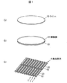
図1(a)〜(c)は、第1の実施の形態に係る発光素子1の製造工程を概略的に表す斜視図である。
このとき、樹脂膜20を完全に切断するため、透明基板11を僅かに削る程度の位置まで刃を入れることが好ましい。
第2の実施の形態は、クリア層が蛍光体含有層の側面を覆うように形成される点において、第1の実施の形態と異なる。なお、第1の実施の形態と同様の点については、説明を省略又は簡略化する。
第3の実施の形態は、第1、2の実施の形態に係る発光素子を有する発光装置についての形態である。なお、第1、2の実施の形態と同様の点については、説明を省略又は簡略化する。
上記実施の形態に係る発光装置によれば、複数の発光素子に含まれる蛍光体含有層を一括して形成するため、発光素子間の発光色のばらつきが小さい。また、個片化された発光素子の各々に蛍光体含有層を貼り付ける場合のように接着剤を使用する必要がないため、製造コストを低減することができる。
3 発光装置
10 ウエハ
11 透明基板
12 発光部
20 樹脂膜
21 蛍光体含有層
22 クリア層
31 基板
34 側壁
Claims (5)
- 透明基板とその上に形成された複数の発光部からなるウェハの、前記透明基板の前記複数の発光部が形成された面と反対側の面に、蛍光体含有層を含む樹脂膜を形成する工程と、
前記樹脂膜を形成する前又は後に、スクライビングにより前記透明基板の前記複数の発光部が形成された面に分離予定面に沿ってスクライビングラインを形成する工程と、
前記スクライビングラインを形成する前又は後に、前記分離予定面に沿って前記樹脂膜を切断する工程と、
前記スクライビングラインを形成し、かつ前記樹脂膜を切断した後、ブレイキングにより前記分離予定面に沿って前記透明基板を分離する工程と、
を含む、発光素子の製造方法。 - 前記樹脂膜が、前記蛍光体含有層上のクリア層有する、
請求項1に記載の発光素子の製造方法。 - 前記クリア層が、前記蛍光体含有層の上面及び側面を覆うように形成される、
請求項2に記載の発光素子の製造方法。 - 前記クリア層の屈折率が前記蛍光体含有層の屈折率よりも低い、
請求項2又は3に記載の発光素子の製造方法。 - 請求項1〜4のいずれか1項に記載の発光素子の製造方法により製造された発光素子を基板上にフリップチップ実装する工程と、
フリップチップ実装された前記発光素子の側面を覆うように白色の側壁を形成する工程と、
を含む、発光装置の製造方法。
Priority Applications (2)
| Application Number | Priority Date | Filing Date | Title |
|---|---|---|---|
| JP2016057610A JP6593237B2 (ja) | 2016-03-22 | 2016-03-22 | 発光素子の製造方法、及び発光装置の製造方法 |
| US15/446,968 US10096585B2 (en) | 2016-03-22 | 2017-03-01 | Method of manufacturing light emitting element and light emitting device including forming resin film including phosphor containing layer |
Applications Claiming Priority (1)
| Application Number | Priority Date | Filing Date | Title |
|---|---|---|---|
| JP2016057610A JP6593237B2 (ja) | 2016-03-22 | 2016-03-22 | 発光素子の製造方法、及び発光装置の製造方法 |
Publications (2)
| Publication Number | Publication Date |
|---|---|
| JP2017174909A JP2017174909A (ja) | 2017-09-28 |
| JP6593237B2 true JP6593237B2 (ja) | 2019-10-23 |
Family
ID=59898235
Family Applications (1)
| Application Number | Title | Priority Date | Filing Date |
|---|---|---|---|
| JP2016057610A Active JP6593237B2 (ja) | 2016-03-22 | 2016-03-22 | 発光素子の製造方法、及び発光装置の製造方法 |
Country Status (2)
| Country | Link |
|---|---|
| US (1) | US10096585B2 (ja) |
| JP (1) | JP6593237B2 (ja) |
Families Citing this family (15)
| Publication number | Priority date | Publication date | Assignee | Title |
|---|---|---|---|---|
| US11302248B2 (en) | 2019-01-29 | 2022-04-12 | Osram Opto Semiconductors Gmbh | U-led, u-led device, display and method for the same |
| CN121583214A (zh) | 2019-01-29 | 2026-02-27 | 奥斯兰姆奥普托半导体股份有限两合公司 | 视频墙、驱动器电路、控制系统及其方法 |
| US11271143B2 (en) | 2019-01-29 | 2022-03-08 | Osram Opto Semiconductors Gmbh | μ-LED, μ-LED device, display and method for the same |
| US11610868B2 (en) | 2019-01-29 | 2023-03-21 | Osram Opto Semiconductors Gmbh | μ-LED, μ-LED device, display and method for the same |
| US11156759B2 (en) | 2019-01-29 | 2021-10-26 | Osram Opto Semiconductors Gmbh | μ-LED, μ-LED device, display and method for the same |
| WO2020229576A2 (de) | 2019-05-14 | 2020-11-19 | Osram Opto Semiconductors Gmbh | Beleuchtungseinheit, verfahren zur herstellung einer beleuchtungseinheit, konverterelement für ein opto-elektronisches bauelement, strahlungsquelle mit einer led und einem konverterelement, auskoppelstruktur, und optoelektronische vorrichtung |
| KR20210120106A (ko) | 2019-02-11 | 2021-10-06 | 오스람 옵토 세미컨덕터스 게엠베하 | 광전자 부품, 광전자 조립체 및 방법 |
| JP7604394B2 (ja) | 2019-04-23 | 2024-12-23 | エイエムエス-オスラム インターナショナル ゲーエムベーハー | Ledモジュール、ledディスプレイモジュール、および当該モジュールを製造する方法 |
| US11538852B2 (en) * | 2019-04-23 | 2022-12-27 | Osram Opto Semiconductors Gmbh | μ-LED, μ-LED device, display and method for the same |
| KR102947058B1 (ko) | 2019-05-13 | 2026-04-01 | 에이엠에스-오스람 인터내셔널 게엠베하 | 다중 칩 캐리어 구조체 |
| WO2020233873A1 (de) | 2019-05-23 | 2020-11-26 | Osram Opto Semiconductors Gmbh | Beleuchtungsanordnung, lichtführungsanordnung und verfahren |
| JP7169513B2 (ja) | 2019-12-23 | 2022-11-11 | 日亜化学工業株式会社 | 発光素子の製造方法 |
| US11646392B2 (en) * | 2020-06-09 | 2023-05-09 | Nichia Corporation | Method of manufacturing light-emitting device |
| JP7089204B2 (ja) * | 2020-06-09 | 2022-06-22 | 日亜化学工業株式会社 | 発光装置の製造方法 |
| CN113097367A (zh) * | 2021-03-24 | 2021-07-09 | 深圳市华星光电半导体显示技术有限公司 | QD-miniLED显示面板及其制备方法 |
Family Cites Families (20)
| Publication number | Priority date | Publication date | Assignee | Title |
|---|---|---|---|---|
| JP3449201B2 (ja) * | 1997-11-28 | 2003-09-22 | 日亜化学工業株式会社 | 窒化物半導体素子の製造方法 |
| JP4081985B2 (ja) | 2001-03-02 | 2008-04-30 | 日亜化学工業株式会社 | 発光装置およびその製造方法 |
| JP4122739B2 (ja) * | 2001-07-26 | 2008-07-23 | 松下電工株式会社 | 発光素子及びその製造方法 |
| US9159888B2 (en) * | 2007-01-22 | 2015-10-13 | Cree, Inc. | Wafer level phosphor coating method and devices fabricated utilizing method |
| US7994531B2 (en) | 2009-04-02 | 2011-08-09 | Visera Technologies Company Limited | White-light light emitting diode chips and fabrication methods thereof |
| US20100327733A1 (en) * | 2009-06-25 | 2010-12-30 | Bridgelux, Inc. | Multiple layer phosphor bearing film |
| US8329482B2 (en) * | 2010-04-30 | 2012-12-11 | Cree, Inc. | White-emitting LED chips and method for making same |
| JP2012164902A (ja) * | 2011-02-09 | 2012-08-30 | Citizen Holdings Co Ltd | 半導体発光装置の製造方法 |
| JP5840377B2 (ja) * | 2011-04-14 | 2016-01-06 | 日東電工株式会社 | 反射樹脂シートおよび発光ダイオード装置の製造方法 |
| JP2013211399A (ja) * | 2012-03-30 | 2013-10-10 | Toshiba Corp | 半導体発光素子 |
| JP2013258209A (ja) | 2012-06-11 | 2013-12-26 | Nitto Denko Corp | 封止シート、発光ダイオード装置およびその製造方法 |
| US9082940B2 (en) | 2012-06-29 | 2015-07-14 | Nitto Denko Corporation | Encapsulating layer-covered semiconductor element, producing method thereof, and semiconductor device |
| JP2014022704A (ja) | 2012-07-24 | 2014-02-03 | Toray Ind Inc | 蛍光体含有樹脂シートと発光装置及びその製造方法 |
| KR20140032691A (ko) * | 2012-09-07 | 2014-03-17 | 일진엘이디(주) | 발광 소자 및 그 제조 방법 |
| JP2014165320A (ja) * | 2013-02-25 | 2014-09-08 | Citizen Electronics Co Ltd | Led装置の製造方法 |
| JP2014192326A (ja) | 2013-03-27 | 2014-10-06 | Nitto Denko Corp | 光半導体装置の製造方法 |
| JP6387780B2 (ja) * | 2013-10-28 | 2018-09-12 | 日亜化学工業株式会社 | 発光装置及びその製造方法 |
| JP5702481B2 (ja) | 2014-03-03 | 2015-04-15 | スタンレー電気株式会社 | 発光装置およびその製造方法 |
| KR102145208B1 (ko) * | 2014-06-10 | 2020-08-19 | 삼성전자주식회사 | 발광소자 패키지 제조방법 |
| TW201717334A (zh) * | 2015-11-05 | 2017-05-16 | 凌北卿 | 封裝結構及其製法 |
-
2016
- 2016-03-22 JP JP2016057610A patent/JP6593237B2/ja active Active
-
2017
- 2017-03-01 US US15/446,968 patent/US10096585B2/en active Active
Also Published As
| Publication number | Publication date |
|---|---|
| US10096585B2 (en) | 2018-10-09 |
| US20170278834A1 (en) | 2017-09-28 |
| JP2017174909A (ja) | 2017-09-28 |
Similar Documents
| Publication | Publication Date | Title |
|---|---|---|
| JP6593237B2 (ja) | 発光素子の製造方法、及び発光装置の製造方法 | |
| US11056627B2 (en) | Light emitting device | |
| JP6288009B2 (ja) | 発光装置の製造方法 | |
| JP6187277B2 (ja) | 発光装置及びその製造方法 | |
| JP6176171B2 (ja) | 発光装置の製造方法 | |
| JP5661552B2 (ja) | 半導体発光装置及びその製造方法 | |
| JP6500255B2 (ja) | 発光装置の製造方法 | |
| TWI542047B (zh) | 發光二極體封裝結構之製法 | |
| JP2012199411A (ja) | 発光装置 | |
| CN105990501B (zh) | 发光装置和用于制造发光装置的方法 | |
| US20170025584A1 (en) | Color-converting substrate for light-emitting diode and method for producing same | |
| JP6511809B2 (ja) | 発光装置及びその実装方法、並びに光源装置の製造方法 | |
| JP2017022305A (ja) | 発光装置の製造方法 | |
| JP2015026753A (ja) | 半導体発光装置及びその製造方法 | |
| JP6194514B2 (ja) | 発光装置の製造方法 | |
| JP2022008965A (ja) | 発光装置の製造方法 | |
| JP2019134187A (ja) | 発光装置の製造方法 | |
| JP2016072475A (ja) | セラミックスパッケージ、発光装置及びそれらの製造方法 | |
| JP2019212695A (ja) | キャップの製造方法と、発光装置及びその製造方法 | |
| JP7393617B2 (ja) | 発光装置、及びその製造方法 | |
| JP7381848B2 (ja) | 発光装置及びその製造方法 | |
| JP2017005247A (ja) | 発光装置の製造方法及び発光装置 | |
| JP2020167378A (ja) | 発光装置の製造方法 | |
| JP2015111626A (ja) | 発光装置およびその製造方法 | |
| JP2018073975A (ja) | 発光装置の製造方法 |
Legal Events
| Date | Code | Title | Description |
|---|---|---|---|
| A621 | Written request for application examination |
Free format text: JAPANESE INTERMEDIATE CODE: A621 Effective date: 20180423 |
|
| A977 | Report on retrieval |
Free format text: JAPANESE INTERMEDIATE CODE: A971007 Effective date: 20190208 |
|
| A131 | Notification of reasons for refusal |
Free format text: JAPANESE INTERMEDIATE CODE: A131 Effective date: 20190312 |
|
| A521 | Request for written amendment filed |
Free format text: JAPANESE INTERMEDIATE CODE: A523 Effective date: 20190510 |
|
| RD02 | Notification of acceptance of power of attorney |
Free format text: JAPANESE INTERMEDIATE CODE: A7422 Effective date: 20190510 |
|
| TRDD | Decision of grant or rejection written | ||
| A01 | Written decision to grant a patent or to grant a registration (utility model) |
Free format text: JAPANESE INTERMEDIATE CODE: A01 Effective date: 20190827 |
|
| A61 | First payment of annual fees (during grant procedure) |
Free format text: JAPANESE INTERMEDIATE CODE: A61 Effective date: 20190909 |
|
| R150 | Certificate of patent or registration of utility model |
Ref document number: 6593237 Country of ref document: JP Free format text: JAPANESE INTERMEDIATE CODE: R150 |