JP6719090B2 - 半導体素子 - Google Patents
半導体素子 Download PDFInfo
- Publication number
- JP6719090B2 JP6719090B2 JP2016245590A JP2016245590A JP6719090B2 JP 6719090 B2 JP6719090 B2 JP 6719090B2 JP 2016245590 A JP2016245590 A JP 2016245590A JP 2016245590 A JP2016245590 A JP 2016245590A JP 6719090 B2 JP6719090 B2 JP 6719090B2
- Authority
- JP
- Japan
- Prior art keywords
- region
- semiconductor
- layer
- surface electrode
- semiconductor element
- Prior art date
- Legal status (The legal status is an assumption and is not a legal conclusion. Google has not performed a legal analysis and makes no representation as to the accuracy of the status listed.)
- Expired - Fee Related
Links
Images






Classifications
-
- H—ELECTRICITY
- H10—SEMICONDUCTOR DEVICES; ELECTRIC SOLID-STATE DEVICES NOT OTHERWISE PROVIDED FOR
- H10W—GENERIC PACKAGES, INTERCONNECTIONS, CONNECTORS OR OTHER CONSTRUCTIONAL DETAILS OF DEVICES COVERED BY CLASS H10
- H10W74/00—Encapsulations, e.g. protective coatings
- H10W74/10—Encapsulations, e.g. protective coatings characterised by their shape or disposition
- H10W74/131—Encapsulations, e.g. protective coatings characterised by their shape or disposition the semiconductor body being only partially enclosed
- H10W74/137—Encapsulations, e.g. protective coatings characterised by their shape or disposition the semiconductor body being only partially enclosed the encapsulations being directly on the semiconductor body
-
- H—ELECTRICITY
- H10—SEMICONDUCTOR DEVICES; ELECTRIC SOLID-STATE DEVICES NOT OTHERWISE PROVIDED FOR
- H10D—INORGANIC ELECTRIC SEMICONDUCTOR DEVICES
- H10D30/00—Field-effect transistors [FET]
- H10D30/60—Insulated-gate field-effect transistors [IGFET]
- H10D30/64—Double-diffused metal-oxide semiconductor [DMOS] FETs
- H10D30/66—Vertical DMOS [VDMOS] FETs
- H10D30/665—Vertical DMOS [VDMOS] FETs having edge termination structures
-
- H—ELECTRICITY
- H10—SEMICONDUCTOR DEVICES; ELECTRIC SOLID-STATE DEVICES NOT OTHERWISE PROVIDED FOR
- H10D—INORGANIC ELECTRIC SEMICONDUCTOR DEVICES
- H10D62/00—Semiconductor bodies, or regions thereof, of devices having potential barriers
- H10D62/10—Shapes, relative sizes or dispositions of the regions of the semiconductor bodies; Shapes of the semiconductor bodies
- H10D62/102—Constructional design considerations for preventing surface leakage or controlling electric field concentration
- H10D62/103—Constructional design considerations for preventing surface leakage or controlling electric field concentration for increasing or controlling the breakdown voltage of reverse-biased devices
- H10D62/105—Constructional design considerations for preventing surface leakage or controlling electric field concentration for increasing or controlling the breakdown voltage of reverse-biased devices by having particular doping profiles, shapes or arrangements of PN junctions; by having supplementary regions, e.g. junction termination extension [JTE]
-
- H—ELECTRICITY
- H10—SEMICONDUCTOR DEVICES; ELECTRIC SOLID-STATE DEVICES NOT OTHERWISE PROVIDED FOR
- H10D—INORGANIC ELECTRIC SEMICONDUCTOR DEVICES
- H10D62/00—Semiconductor bodies, or regions thereof, of devices having potential barriers
- H10D62/10—Shapes, relative sizes or dispositions of the regions of the semiconductor bodies; Shapes of the semiconductor bodies
- H10D62/102—Constructional design considerations for preventing surface leakage or controlling electric field concentration
- H10D62/103—Constructional design considerations for preventing surface leakage or controlling electric field concentration for increasing or controlling the breakdown voltage of reverse-biased devices
- H10D62/105—Constructional design considerations for preventing surface leakage or controlling electric field concentration for increasing or controlling the breakdown voltage of reverse-biased devices by having particular doping profiles, shapes or arrangements of PN junctions; by having supplementary regions, e.g. junction termination extension [JTE]
- H10D62/106—Constructional design considerations for preventing surface leakage or controlling electric field concentration for increasing or controlling the breakdown voltage of reverse-biased devices by having particular doping profiles, shapes or arrangements of PN junctions; by having supplementary regions, e.g. junction termination extension [JTE] having supplementary regions doped oppositely to or in rectifying contact with regions of the semiconductor bodies, e.g. guard rings with PN or Schottky junctions
-
- H—ELECTRICITY
- H10—SEMICONDUCTOR DEVICES; ELECTRIC SOLID-STATE DEVICES NOT OTHERWISE PROVIDED FOR
- H10D—INORGANIC ELECTRIC SEMICONDUCTOR DEVICES
- H10D62/00—Semiconductor bodies, or regions thereof, of devices having potential barriers
- H10D62/10—Shapes, relative sizes or dispositions of the regions of the semiconductor bodies; Shapes of the semiconductor bodies
- H10D62/102—Constructional design considerations for preventing surface leakage or controlling electric field concentration
- H10D62/103—Constructional design considerations for preventing surface leakage or controlling electric field concentration for increasing or controlling the breakdown voltage of reverse-biased devices
- H10D62/105—Constructional design considerations for preventing surface leakage or controlling electric field concentration for increasing or controlling the breakdown voltage of reverse-biased devices by having particular doping profiles, shapes or arrangements of PN junctions; by having supplementary regions, e.g. junction termination extension [JTE]
- H10D62/106—Constructional design considerations for preventing surface leakage or controlling electric field concentration for increasing or controlling the breakdown voltage of reverse-biased devices by having particular doping profiles, shapes or arrangements of PN junctions; by having supplementary regions, e.g. junction termination extension [JTE] having supplementary regions doped oppositely to or in rectifying contact with regions of the semiconductor bodies, e.g. guard rings with PN or Schottky junctions
- H10D62/107—Buried supplementary regions, e.g. buried guard rings
-
- H—ELECTRICITY
- H10—SEMICONDUCTOR DEVICES; ELECTRIC SOLID-STATE DEVICES NOT OTHERWISE PROVIDED FOR
- H10D—INORGANIC ELECTRIC SEMICONDUCTOR DEVICES
- H10D62/00—Semiconductor bodies, or regions thereof, of devices having potential barriers
- H10D62/80—Semiconductor bodies, or regions thereof, of devices having potential barriers characterised by the materials
- H10D62/83—Semiconductor bodies, or regions thereof, of devices having potential barriers characterised by the materials being Group IV materials, e.g. B-doped Si or undoped Ge
- H10D62/832—Semiconductor bodies, or regions thereof, of devices having potential barriers characterised by the materials being Group IV materials, e.g. B-doped Si or undoped Ge being Group IV materials comprising two or more elements, e.g. SiGe
- H10D62/8325—Silicon carbide
-
- H—ELECTRICITY
- H10—SEMICONDUCTOR DEVICES; ELECTRIC SOLID-STATE DEVICES NOT OTHERWISE PROVIDED FOR
- H10D—INORGANIC ELECTRIC SEMICONDUCTOR DEVICES
- H10D8/00—Diodes
- H10D8/01—Manufacture or treatment
- H10D8/051—Manufacture or treatment of Schottky diodes
-
- H—ELECTRICITY
- H10—SEMICONDUCTOR DEVICES; ELECTRIC SOLID-STATE DEVICES NOT OTHERWISE PROVIDED FOR
- H10D—INORGANIC ELECTRIC SEMICONDUCTOR DEVICES
- H10D8/00—Diodes
- H10D8/60—Schottky-barrier diodes
-
- H—ELECTRICITY
- H10—SEMICONDUCTOR DEVICES; ELECTRIC SOLID-STATE DEVICES NOT OTHERWISE PROVIDED FOR
- H10D—INORGANIC ELECTRIC SEMICONDUCTOR DEVICES
- H10D12/00—Bipolar devices controlled by the field effect, e.g. insulated-gate bipolar transistors [IGBT]
- H10D12/411—Insulated-gate bipolar transistors [IGBT]
- H10D12/441—Vertical IGBTs
-
- H—ELECTRICITY
- H10—SEMICONDUCTOR DEVICES; ELECTRIC SOLID-STATE DEVICES NOT OTHERWISE PROVIDED FOR
- H10D—INORGANIC ELECTRIC SEMICONDUCTOR DEVICES
- H10D30/00—Field-effect transistors [FET]
- H10D30/60—Insulated-gate field-effect transistors [IGFET]
- H10D30/64—Double-diffused metal-oxide semiconductor [DMOS] FETs
- H10D30/66—Vertical DMOS [VDMOS] FETs
-
- H—ELECTRICITY
- H10—SEMICONDUCTOR DEVICES; ELECTRIC SOLID-STATE DEVICES NOT OTHERWISE PROVIDED FOR
- H10D—INORGANIC ELECTRIC SEMICONDUCTOR DEVICES
- H10D62/00—Semiconductor bodies, or regions thereof, of devices having potential barriers
- H10D62/10—Shapes, relative sizes or dispositions of the regions of the semiconductor bodies; Shapes of the semiconductor bodies
- H10D62/102—Constructional design considerations for preventing surface leakage or controlling electric field concentration
- H10D62/103—Constructional design considerations for preventing surface leakage or controlling electric field concentration for increasing or controlling the breakdown voltage of reverse-biased devices
- H10D62/105—Constructional design considerations for preventing surface leakage or controlling electric field concentration for increasing or controlling the breakdown voltage of reverse-biased devices by having particular doping profiles, shapes or arrangements of PN junctions; by having supplementary regions, e.g. junction termination extension [JTE]
- H10D62/109—Reduced surface field [RESURF] PN junction structures
-
- H—ELECTRICITY
- H10—SEMICONDUCTOR DEVICES; ELECTRIC SOLID-STATE DEVICES NOT OTHERWISE PROVIDED FOR
- H10W—GENERIC PACKAGES, INTERCONNECTIONS, CONNECTORS OR OTHER CONSTRUCTIONAL DETAILS OF DEVICES COVERED BY CLASS H10
- H10W42/00—Arrangements for protection of devices
- H10W42/121—Arrangements for protection of devices protecting against mechanical damage
-
- H—ELECTRICITY
- H10—SEMICONDUCTOR DEVICES; ELECTRIC SOLID-STATE DEVICES NOT OTHERWISE PROVIDED FOR
- H10W—GENERIC PACKAGES, INTERCONNECTIONS, CONNECTORS OR OTHER CONSTRUCTIONAL DETAILS OF DEVICES COVERED BY CLASS H10
- H10W72/00—Interconnections or connectors in packages
- H10W72/071—Connecting or disconnecting
- H10W72/073—Connecting or disconnecting of die-attach connectors
- H10W72/07351—Connecting or disconnecting of die-attach connectors characterised by changes in properties of the die-attach connectors during connecting
- H10W72/07354—Connecting or disconnecting of die-attach connectors characterised by changes in properties of the die-attach connectors during connecting changes in dispositions
-
- H—ELECTRICITY
- H10—SEMICONDUCTOR DEVICES; ELECTRIC SOLID-STATE DEVICES NOT OTHERWISE PROVIDED FOR
- H10W—GENERIC PACKAGES, INTERCONNECTIONS, CONNECTORS OR OTHER CONSTRUCTIONAL DETAILS OF DEVICES COVERED BY CLASS H10
- H10W72/00—Interconnections or connectors in packages
- H10W72/30—Die-attach connectors
- H10W72/341—Dispositions of die-attach connectors, e.g. layouts
- H10W72/347—Dispositions of multiple die-attach connectors
-
- H—ELECTRICITY
- H10—SEMICONDUCTOR DEVICES; ELECTRIC SOLID-STATE DEVICES NOT OTHERWISE PROVIDED FOR
- H10W—GENERIC PACKAGES, INTERCONNECTIONS, CONNECTORS OR OTHER CONSTRUCTIONAL DETAILS OF DEVICES COVERED BY CLASS H10
- H10W72/00—Interconnections or connectors in packages
- H10W72/50—Bond wires
- H10W72/531—Shapes of wire connectors
- H10W72/5363—Shapes of wire connectors the connected ends being wedge-shaped
-
- H—ELECTRICITY
- H10—SEMICONDUCTOR DEVICES; ELECTRIC SOLID-STATE DEVICES NOT OTHERWISE PROVIDED FOR
- H10W—GENERIC PACKAGES, INTERCONNECTIONS, CONNECTORS OR OTHER CONSTRUCTIONAL DETAILS OF DEVICES COVERED BY CLASS H10
- H10W72/00—Interconnections or connectors in packages
- H10W72/50—Bond wires
- H10W72/551—Materials of bond wires
- H10W72/552—Materials of bond wires comprising metals or metalloids, e.g. silver
- H10W72/5524—Materials of bond wires comprising metals or metalloids, e.g. silver comprising aluminium [Al]
-
- H—ELECTRICITY
- H10—SEMICONDUCTOR DEVICES; ELECTRIC SOLID-STATE DEVICES NOT OTHERWISE PROVIDED FOR
- H10W—GENERIC PACKAGES, INTERCONNECTIONS, CONNECTORS OR OTHER CONSTRUCTIONAL DETAILS OF DEVICES COVERED BY CLASS H10
- H10W72/00—Interconnections or connectors in packages
- H10W72/851—Dispositions of multiple connectors or interconnections
- H10W72/874—On different surfaces
- H10W72/884—Die-attach connectors and bond wires
-
- H—ELECTRICITY
- H10—SEMICONDUCTOR DEVICES; ELECTRIC SOLID-STATE DEVICES NOT OTHERWISE PROVIDED FOR
- H10W—GENERIC PACKAGES, INTERCONNECTIONS, CONNECTORS OR OTHER CONSTRUCTIONAL DETAILS OF DEVICES COVERED BY CLASS H10
- H10W72/00—Interconnections or connectors in packages
- H10W72/90—Bond pads, in general
- H10W72/921—Structures or relative sizes of bond pads
- H10W72/926—Multiple bond pads having different sizes
-
- H—ELECTRICITY
- H10—SEMICONDUCTOR DEVICES; ELECTRIC SOLID-STATE DEVICES NOT OTHERWISE PROVIDED FOR
- H10W—GENERIC PACKAGES, INTERCONNECTIONS, CONNECTORS OR OTHER CONSTRUCTIONAL DETAILS OF DEVICES COVERED BY CLASS H10
- H10W72/00—Interconnections or connectors in packages
- H10W72/90—Bond pads, in general
- H10W72/981—Auxiliary members, e.g. spacers
- H10W72/983—Reinforcing structures, e.g. collars
-
- H—ELECTRICITY
- H10—SEMICONDUCTOR DEVICES; ELECTRIC SOLID-STATE DEVICES NOT OTHERWISE PROVIDED FOR
- H10W—GENERIC PACKAGES, INTERCONNECTIONS, CONNECTORS OR OTHER CONSTRUCTIONAL DETAILS OF DEVICES COVERED BY CLASS H10
- H10W74/00—Encapsulations, e.g. protective coatings
-
- H—ELECTRICITY
- H10—SEMICONDUCTOR DEVICES; ELECTRIC SOLID-STATE DEVICES NOT OTHERWISE PROVIDED FOR
- H10W—GENERIC PACKAGES, INTERCONNECTIONS, CONNECTORS OR OTHER CONSTRUCTIONAL DETAILS OF DEVICES COVERED BY CLASS H10
- H10W74/00—Encapsulations, e.g. protective coatings
- H10W74/10—Encapsulations, e.g. protective coatings characterised by their shape or disposition
- H10W74/131—Encapsulations, e.g. protective coatings characterised by their shape or disposition the semiconductor body being only partially enclosed
- H10W74/147—Encapsulations, e.g. protective coatings characterised by their shape or disposition the semiconductor body being only partially enclosed the encapsulations being multilayered
-
- H—ELECTRICITY
- H10—SEMICONDUCTOR DEVICES; ELECTRIC SOLID-STATE DEVICES NOT OTHERWISE PROVIDED FOR
- H10W—GENERIC PACKAGES, INTERCONNECTIONS, CONNECTORS OR OTHER CONSTRUCTIONAL DETAILS OF DEVICES COVERED BY CLASS H10
- H10W90/00—Package configurations
- H10W90/701—Package configurations characterised by the relative positions of pads or connectors relative to package parts
- H10W90/731—Package configurations characterised by the relative positions of pads or connectors relative to package parts of die-attach connectors
- H10W90/736—Package configurations characterised by the relative positions of pads or connectors relative to package parts of die-attach connectors between a chip and a stacked lead frame, conducting package substrate or heat sink
-
- H—ELECTRICITY
- H10—SEMICONDUCTOR DEVICES; ELECTRIC SOLID-STATE DEVICES NOT OTHERWISE PROVIDED FOR
- H10W—GENERIC PACKAGES, INTERCONNECTIONS, CONNECTORS OR OTHER CONSTRUCTIONAL DETAILS OF DEVICES COVERED BY CLASS H10
- H10W90/00—Package configurations
- H10W90/701—Package configurations characterised by the relative positions of pads or connectors relative to package parts
- H10W90/751—Package configurations characterised by the relative positions of pads or connectors relative to package parts of bond wires
- H10W90/756—Package configurations characterised by the relative positions of pads or connectors relative to package parts of bond wires between a chip and a stacked lead frame, conducting package substrate or heat sink
Landscapes
- Electrodes Of Semiconductors (AREA)
- Internal Circuitry In Semiconductor Integrated Circuit Devices (AREA)
Description
以下、図面を参照しながら、本開示の半導体素子の第1の実施形態について説明する。本実施形態では、第1導電型がn型、第2導電型がp型である例について示すが、これに限定されない。本開示の実施形態において、第1導電型がp型、第2導電型がn型であってもよい。
以下、ショットキーバリアダイオードを例に、本実施形態の半導体素子をより具体的に説明する。
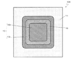
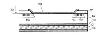
図3Aおよび図3Bは、それぞれ、本実施形態の他の半導体素子1010の断面図および上面図である。図3Aおよび図3Bでは、図2Aおよび図2Bに示す半導体素子1000と同様の構成要素には同じ参照符号を付している。以下、半導体素子1000と同様の構成については説明を省略し、異なる点を主に説明する。
ここで、絶縁層を有しない比較例の半導体素子と比較して、本実施形態の半導体素子1000、1010の効果を説明する。
図6から図16を参照しながら、本実施形態に係る半導体素子1000および1010の製造方法を説明する。図6から図16は、それぞれ、半導体素子1000および1010の製造方法を説明するための工程断面図である。
以下、図面を参照しながら、本開示の半導体素子の第2の実施形態を説明する。本実施形態の半導体素子は、複数の表面電極を備える。以下、SiCを用いた縦型MISFETを例に、本実施形態の半導体素子の構成を説明する。
11 :半導体
13、112、312、313 :表面電極
13a、112a、312a、313a :第1領域
13b、112b、312b、313b :第2領域
15、114、314 :保護層
15p、114p、314p :第1開口部
17、115、315、316 :絶縁層
17p、115p、315p :第2開口部
19、116、317、318 :金属層
19a、116a、317a、318a :第1部分
19b、116b、317b、318b :第2部分
101 :半導体基板
102 :ドリフト層
110 :第2電極
111 :絶縁膜
113 :裏面電極
150、300E :終端領域
151 :ガードリング領域
152 :FLR領域
159 :第1電極
191 :バッファ層
301 :炭化珪素基板
302 :第1炭化珪素半導体層
303 :第1ボディ領域
304 :ソース領域
305 :第1コンタクト領域
306 :第2炭化珪素半導体層
307 :ゲート絶縁膜
308 :ゲート電極
309 :ソース電極
310 :ドレイン電極
311 :層間絶縁膜
401、402、407 :金属導体
403、406 :はんだ
404 :金属ワイヤ
405 :封止材
GP :ゲートパッド領域
SP :ソースパッド領域
Claims (13)
- 所定の素子領域を有する半導体と、
前記素子領域の端部において、前記半導体に配置された電界緩和構造と、
前記半導体の上に配置され、かつ、前記半導体の法線方向から見たとき、前記電界緩和構造の内側に位置する、少なくとも1つの表面電極と、
前記電界緩和構造と前記少なくとも1つの表面電極の周縁部とを覆い、かつ、前記少なくとも1つの表面電極上に開口部を有する保護層と、
前記少なくとも1つの表面電極上において、前記開口部の内側に、前記保護層と離間し、かつ、前記半導体の法線方向から見たとき、前記少なくとも1つの表面電極の第1領域を包囲するように配置された絶縁層と、
前記少なくとも1つの表面電極のうち前記保護層および前記絶縁層のいずれにも覆われていない領域上に配置された金属層と
を備え、
前記金属層は、少なくとも前記第1領域上に配置されている、半導体素子。 - 前記保護層および前記絶縁層は同一材料からなる、請求項1に記載の半導体素子。
- 前記半導体素子はダイオードであり、
前記少なくとも1つの表面電極は、カソードおよびアノードの少なくとも一方を含む、請求項1または2に記載の半導体素子。 - 前記半導体素子はトランジスタであり、
前記少なくとも1つの表面電極は、ソースおよびドレインの少なくとも一方を含む、請求項1または2に記載の半導体素子。 - 前記半導体素子はトランジスタであり、
前記少なくとも1つの表面電極は、エミッタおよびコレクタの少なくとも一方を含む、請求項1または2に記載の半導体素子。 - 前記半導体素子はトランジスタであり、
前記少なくとも1つの表面電極は、ゲートを含む、請求項1または2に記載の半導体素子。 - 前記少なくとも1つの表面電極は、主電流経路以外に設けられた電極を含む、請求項1または2に記載の半導体素子。
- 前記少なくとも1つの表面電極は、前記半導体の法線方向から見たとき、前記絶縁層によって包囲された前記第1領域と、前記保護層と前記絶縁層との間に位置する第2領域とを含み、
前記金属層は、前記第1領域上に位置する第1部分と、前記第2領域上に位置する第2部分とを含む、請求項1から7のいずれかに記載の半導体素子。 - 前記金属層の前記第1部分と前記第2部分とは、互いに分離されている、請求項8に記載の半導体素子。
- 前記金属層は、前記保護層の側面および前記絶縁層の側面と接している、請求項1から9のいずれかに記載の半導体素子。
- 前記金属層は前記少なくとも1つの表面電極よりも高い硬度を有する、請求項1から10のいずれかに記載の半導体素子。
- 前記少なくとも1つの表面電極は主にアルミニウムを含有し、前記金属層は主にニッケルを含有する、請求項11に記載の半導体素子。
- 前記半導体は炭化珪素を含む、請求項1から12のいずれかに記載の半導体素子。
Priority Applications (2)
| Application Number | Priority Date | Filing Date | Title |
|---|---|---|---|
| JP2016245590A JP6719090B2 (ja) | 2016-12-19 | 2016-12-19 | 半導体素子 |
| US15/834,035 US10276470B2 (en) | 2016-12-19 | 2017-12-06 | Semiconductor device having an electric field relaxation structure |
Applications Claiming Priority (1)
| Application Number | Priority Date | Filing Date | Title |
|---|---|---|---|
| JP2016245590A JP6719090B2 (ja) | 2016-12-19 | 2016-12-19 | 半導体素子 |
Publications (2)
| Publication Number | Publication Date |
|---|---|
| JP2018101662A JP2018101662A (ja) | 2018-06-28 |
| JP6719090B2 true JP6719090B2 (ja) | 2020-07-08 |
Family
ID=62556946
Family Applications (1)
| Application Number | Title | Priority Date | Filing Date |
|---|---|---|---|
| JP2016245590A Expired - Fee Related JP6719090B2 (ja) | 2016-12-19 | 2016-12-19 | 半導体素子 |
Country Status (2)
| Country | Link |
|---|---|
| US (1) | US10276470B2 (ja) |
| JP (1) | JP6719090B2 (ja) |
Families Citing this family (16)
| Publication number | Priority date | Publication date | Assignee | Title |
|---|---|---|---|---|
| US10461049B2 (en) * | 2015-12-14 | 2019-10-29 | Mitsubishi Electric Corporation | Semiconductor device and manufacturing method therefor |
| CN110199396B (zh) * | 2017-01-26 | 2022-06-24 | 三菱电机株式会社 | 半导体装置的制造方法 |
| JP7085959B2 (ja) * | 2018-10-22 | 2022-06-17 | 三菱電機株式会社 | 半導体装置 |
| US10892237B2 (en) * | 2018-12-14 | 2021-01-12 | General Electric Company | Methods of fabricating high voltage semiconductor devices having improved electric field suppression |
| US11538769B2 (en) * | 2018-12-14 | 2022-12-27 | General Electric Company | High voltage semiconductor devices having improved electric field suppression |
| GB201909588D0 (en) * | 2019-07-03 | 2019-08-14 | Univ Coventry | A semiconductor device and methods for production thereof |
| JP2022007763A (ja) * | 2020-06-26 | 2022-01-13 | 株式会社デンソー | 半導体装置およびその製造方法 |
| US20230103655A1 (en) * | 2020-06-26 | 2023-04-06 | Rohm Co., Ltd. | Electronic component |
| CN113540229B (zh) * | 2021-06-11 | 2022-07-12 | 中兴通讯股份有限公司 | 半导体器件及其制作方法 |
| JP7770122B2 (ja) * | 2021-07-05 | 2025-11-14 | 三菱電機株式会社 | 半導体装置 |
| JPWO2023032653A1 (ja) * | 2021-09-03 | 2023-03-09 | ||
| IT202200006485A1 (it) * | 2022-04-01 | 2023-10-01 | St Microelectronics Srl | Dispositivo elettronico con oscillazioni di commutazione ridotte |
| US12513922B2 (en) * | 2022-06-24 | 2025-12-30 | The Government Of The United States Of America, As Represented By The Secretary Of The Navy | β-Ga2O3 junction barrier Schottky (JBS) diodes with sputtered p-type NiO |
| JP2024015665A (ja) * | 2022-07-25 | 2024-02-06 | 株式会社デンソー | 半導体装置 |
| EP4439651A1 (en) * | 2023-03-29 | 2024-10-02 | Nexperia B.V. | Zero-stress zones and controlled-fracturing zones in the passivation layer of a semiconductor device |
| CN121772268A (zh) * | 2024-09-23 | 2026-03-31 | 积亚半导体股份有限公司 | 半导体结构及其制造方法 |
Family Cites Families (23)
| Publication number | Priority date | Publication date | Assignee | Title |
|---|---|---|---|---|
| JP2006005166A (ja) * | 2004-06-17 | 2006-01-05 | Matsushita Electric Ind Co Ltd | 半導体装置の製造方法 |
| US7183626B2 (en) * | 2004-11-17 | 2007-02-27 | International Rectifier Corporation | Passivation structure with voltage equalizing loops |
| JP5048273B2 (ja) * | 2006-05-10 | 2012-10-17 | オンセミコンダクター・トレーディング・リミテッド | 絶縁ゲート型半導体装置 |
| JP4189415B2 (ja) * | 2006-06-30 | 2008-12-03 | 株式会社東芝 | 半導体装置 |
| JP4356764B2 (ja) * | 2007-04-18 | 2009-11-04 | 株式会社デンソー | 炭化珪素半導体装置 |
| US20090050899A1 (en) * | 2007-08-23 | 2009-02-26 | National Institute of Advanced Industrial Scinece and Technology | High-output diamond semiconductor element |
| JP5381420B2 (ja) * | 2008-07-22 | 2014-01-08 | 富士電機株式会社 | 半導体装置 |
| CN102792466B (zh) * | 2010-03-08 | 2016-03-16 | 日亚化学工业株式会社 | 半导体发光元件及其制造方法 |
| JP6099298B2 (ja) * | 2011-05-30 | 2017-03-22 | 富士電機株式会社 | SiC半導体デバイス及びその製造方法 |
| JP5999748B2 (ja) * | 2011-08-12 | 2016-09-28 | ルネサスエレクトロニクス株式会社 | パワーmosfet、igbtおよびパワーダイオード |
| US9159784B2 (en) * | 2011-11-17 | 2015-10-13 | Avogy, Inc. | Aluminum gallium nitride etch stop layer for gallium nitride based devices |
| WO2013121532A1 (ja) * | 2012-02-15 | 2013-08-22 | 富士電機株式会社 | ワイドバンドギャップ半導体装置 |
| WO2013136550A1 (ja) * | 2012-03-16 | 2013-09-19 | 三菱電機株式会社 | 半導体装置およびその製造方法 |
| JP6384944B2 (ja) | 2012-05-31 | 2018-09-05 | 富士電機株式会社 | 炭化珪素半導体装置および炭化珪素半導体装置の製造方法 |
| JP2014107499A (ja) * | 2012-11-29 | 2014-06-09 | Sumitomo Electric Ind Ltd | 炭化珪素半導体装置およびその製造方法 |
| JP5772842B2 (ja) * | 2013-01-31 | 2015-09-02 | 株式会社デンソー | 炭化珪素半導体装置 |
| JP6202944B2 (ja) * | 2013-08-28 | 2017-09-27 | 三菱電機株式会社 | 炭化珪素半導体装置およびその製造方法 |
| JP2015220437A (ja) * | 2014-05-21 | 2015-12-07 | 住友電気工業株式会社 | 炭化珪素半導体装置 |
| DE102015207214A1 (de) * | 2014-05-21 | 2015-12-17 | Sumitomo Electric Industries, Ltd. | Siliziumkarbid-Halbleitervorrichtung |
| US10361266B2 (en) * | 2014-06-09 | 2019-07-23 | Panasonic Intellectual Property Management Co., Ltd. | Semiconductor device |
| JP6745458B2 (ja) * | 2015-04-15 | 2020-08-26 | パナソニックIpマネジメント株式会社 | 半導体素子 |
| US9773924B2 (en) * | 2015-04-22 | 2017-09-26 | Panasonic Intellectual Property Management Co., Ltd. | Semiconductor device having barrier region and edge termination region enclosing barrier region |
| JP6592950B2 (ja) * | 2015-04-24 | 2019-10-23 | 富士電機株式会社 | 炭化ケイ素半導体装置の製造方法 |
-
2016
- 2016-12-19 JP JP2016245590A patent/JP6719090B2/ja not_active Expired - Fee Related
-
2017
- 2017-12-06 US US15/834,035 patent/US10276470B2/en active Active
Also Published As
| Publication number | Publication date |
|---|---|
| JP2018101662A (ja) | 2018-06-28 |
| US10276470B2 (en) | 2019-04-30 |
| US20180174938A1 (en) | 2018-06-21 |
Similar Documents
| Publication | Publication Date | Title |
|---|---|---|
| JP6719090B2 (ja) | 半導体素子 | |
| US9252211B2 (en) | Semiconductor device and manufacturing method thereof | |
| KR101230680B1 (ko) | 반도체 장치 및 그 제조 방법 | |
| JP6702911B2 (ja) | 半導体装置およびその製造方法 | |
| US20190371932A1 (en) | Semiconductor device | |
| JP7400487B2 (ja) | 半導体装置 | |
| US11456359B2 (en) | Semiconductor device and method of manufacturing semiconductor device | |
| US11916112B2 (en) | SiC semiconductor device | |
| JP7611155B2 (ja) | 半導体装置 | |
| US11276621B2 (en) | Semiconductor device | |
| US9997603B2 (en) | Semiconductor device and method of manufacturing semiconductor device | |
| JP7404722B2 (ja) | 半導体装置 | |
| US12255227B2 (en) | SiC semiconductor device | |
| JP5943819B2 (ja) | 半導体素子、半導体装置 | |
| JP7129397B2 (ja) | SiC半導体装置 | |
| JP2018120879A (ja) | 半導体装置および半導体装置の製造方法 | |
| JP6664446B2 (ja) | SiC半導体装置 | |
| JP5233158B2 (ja) | 炭化珪素半導体装置 | |
| US20200258991A1 (en) | Semiconductor device and method of manufacturing semiconductor device | |
| JP7243173B2 (ja) | 半導体装置および半導体装置の製造方法 | |
| JP6664445B2 (ja) | SiC半導体装置 | |
| JP7103435B2 (ja) | 半導体装置および半導体装置の製造方法 | |
| JP2020027854A (ja) | SiC半導体装置 | |
| JP7318226B2 (ja) | 半導体装置および半導体装置の製造方法 | |
| US20260068206A1 (en) | Method of manufacturing semiconductor device |
Legal Events
| Date | Code | Title | Description |
|---|---|---|---|
| A621 | Written request for application examination |
Free format text: JAPANESE INTERMEDIATE CODE: A621 Effective date: 20190411 |
|
| A977 | Report on retrieval |
Free format text: JAPANESE INTERMEDIATE CODE: A971007 Effective date: 20200110 |
|
| A131 | Notification of reasons for refusal |
Free format text: JAPANESE INTERMEDIATE CODE: A131 Effective date: 20200121 |
|
| A521 | Request for written amendment filed |
Free format text: JAPANESE INTERMEDIATE CODE: A523 Effective date: 20200218 |
|
| TRDD | Decision of grant or rejection written | ||
| A01 | Written decision to grant a patent or to grant a registration (utility model) |
Free format text: JAPANESE INTERMEDIATE CODE: A01 Effective date: 20200526 |
|
| A61 | First payment of annual fees (during grant procedure) |
Free format text: JAPANESE INTERMEDIATE CODE: A61 Effective date: 20200529 |
|
| R151 | Written notification of patent or utility model registration |
Ref document number: 6719090 Country of ref document: JP Free format text: JAPANESE INTERMEDIATE CODE: R151 |
|
| LAPS | Cancellation because of no payment of annual fees |