JP5381420B2 - 半導体装置 - Google Patents
半導体装置 Download PDFInfo
- Publication number
- JP5381420B2 JP5381420B2 JP2009157894A JP2009157894A JP5381420B2 JP 5381420 B2 JP5381420 B2 JP 5381420B2 JP 2009157894 A JP2009157894 A JP 2009157894A JP 2009157894 A JP2009157894 A JP 2009157894A JP 5381420 B2 JP5381420 B2 JP 5381420B2
- Authority
- JP
- Japan
- Prior art keywords
- diffusion region
- outer peripheral
- anode diffusion
- insulating film
- anode electrode
- Prior art date
- Legal status (The legal status is an assumption and is not a legal conclusion. Google has not performed a legal analysis and makes no representation as to the accuracy of the status listed.)
- Active
Links
Images


Classifications
-
- H—ELECTRICITY
- H10—SEMICONDUCTOR DEVICES; ELECTRIC SOLID-STATE DEVICES NOT OTHERWISE PROVIDED FOR
- H10D—INORGANIC ELECTRIC SEMICONDUCTOR DEVICES
- H10D8/00—Diodes
- H10D8/411—PN diodes having planar bodies
-
- H—ELECTRICITY
- H10—SEMICONDUCTOR DEVICES; ELECTRIC SOLID-STATE DEVICES NOT OTHERWISE PROVIDED FOR
- H10D—INORGANIC ELECTRIC SEMICONDUCTOR DEVICES
- H10D62/00—Semiconductor bodies, or regions thereof, of devices having potential barriers
- H10D62/10—Shapes, relative sizes or dispositions of the regions of the semiconductor bodies; Shapes of the semiconductor bodies
- H10D62/102—Constructional design considerations for preventing surface leakage or controlling electric field concentration
- H10D62/103—Constructional design considerations for preventing surface leakage or controlling electric field concentration for increasing or controlling the breakdown voltage of reverse-biased devices
- H10D62/105—Constructional design considerations for preventing surface leakage or controlling electric field concentration for increasing or controlling the breakdown voltage of reverse-biased devices by having particular doping profiles, shapes or arrangements of PN junctions; by having supplementary regions, e.g. junction termination extension [JTE]
- H10D62/106—Constructional design considerations for preventing surface leakage or controlling electric field concentration for increasing or controlling the breakdown voltage of reverse-biased devices by having particular doping profiles, shapes or arrangements of PN junctions; by having supplementary regions, e.g. junction termination extension [JTE] having supplementary regions doped oppositely to or in rectifying contact with regions of the semiconductor bodies, e.g. guard rings with PN or Schottky junctions
-
- H—ELECTRICITY
- H10—SEMICONDUCTOR DEVICES; ELECTRIC SOLID-STATE DEVICES NOT OTHERWISE PROVIDED FOR
- H10D—INORGANIC ELECTRIC SEMICONDUCTOR DEVICES
- H10D62/00—Semiconductor bodies, or regions thereof, of devices having potential barriers
- H10D62/10—Shapes, relative sizes or dispositions of the regions of the semiconductor bodies; Shapes of the semiconductor bodies
- H10D62/124—Shapes, relative sizes or dispositions of the regions of semiconductor bodies or of junctions between the regions
- H10D62/126—Top-view geometrical layouts of the regions or the junctions
-
- H—ELECTRICITY
- H10—SEMICONDUCTOR DEVICES; ELECTRIC SOLID-STATE DEVICES NOT OTHERWISE PROVIDED FOR
- H10D—INORGANIC ELECTRIC SEMICONDUCTOR DEVICES
- H10D64/00—Electrodes of devices having potential barriers
- H10D64/111—Field plates
- H10D64/112—Field plates comprising multiple field plate segments
Landscapes
- Electrodes Of Semiconductors (AREA)
Description
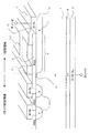
図1〜図9はそれぞれ番号順に対応する本発明の実施例1〜実施例9にかかるダイオードの要部斜視断面図または要部断面図である。図10は電力変換装置を模式的に示す等価回路図である。図11は逆回復耐量を向上させた従来のダイオードの要部斜視断面図である。
重心Oから、前記p型アノード拡散領域2の外周端24が表す多角形の各辺に垂直に線を伸ばしたときの外周端までの距離のうち最短の距離をWACTと呼ぶことにする。例えば、図12の平面図(b)では、前記最短距離は重心Oから紙面に向かって左側にある点線24の辺までの距離が、最短の距離WACTとなる。図18についても同様である。

さらに図15に、同一のαに対して、各βにおける順電圧と、β=0.02、すなわちWCNTが6μmのときの順電圧との差分を△VFと定義して、△VFについてのα依存性をしめす。この図によると、α=0.87のとき、具体的にはWACTが第四金属膜3−5の環状の幅WFFMと同じ長さ程度に十分小さいときは、βが1に近い値、つまり第四金属膜3−5下の開口部17の幅WCNTが同金属膜3−5の幅WFFMに近いほど、順電圧差△VFが大きくなることが明らかになった。すなわち活性領域が狭いほど、第四金属膜3−5下部の静電ポテンシャル分布は活性領域の幅の影響を受けて変化し、その結果順電圧差△VFが変化するということである。この効果は、図17に示すように、半導体デバイスシミュレーションにより得られた電流密度分布と等電位線分布の模式図を用いて説明できる。図17は、半導体デバイスシミュレーションにより得られた電流密度分布と等電位線分布の模式図であり、(b)の断面図と(c)の断面図、および(b)、(c)図中の表面から深さ10μmにある×印の位置における電流密度分布図(a)からなる。(b)の断面図は、β=0.88すなわちWCNT=230μmの場合で、(c)の断面図はβ=0.02すなわちWCNT=6μmの場合に対応する。両断面図に、順方向導通時における1Vステップの4本の等電位線23の分布を示す。(b)の断面図のように、第四金属膜3−5下の開口部17の幅WCNTが十分大きいときは、導通時の開口部17下(周辺部8)の電位(静電ポテンシャル)が、アノード電極よりも低い電位で広く固定される。そのためキャリア(電子、ホール)は、アノード電極3が前記アノード拡散領域2とオーミック接触をしている部分の外周端11より外周部へ侵入することができなくなる。特にWCNTが十分広くかつWACTが小さい場合(つまりαが小さい場合)、電流密度分布図(a)の(1)のように、WCNTが十分狭い場合の(2)に比べて、電流経路の断面が狭くなり、その分だけ活性部分の電流密度が高くなる。その結果、(1)の順電圧降下が(2)の場合よりも高くなり、順電圧差△VFが発生する。一方、WACT(つまりα)が十分大きい場合は、WCNTの影響は小さくなるため、電流密度分布図(a)の(3)もしくは(4)のように、活性領域の電流密度の差は無視できる程度に小さくなる。そのため、順電圧差△VFも十分小さくなる。
2 p型アノード拡散領域
3 アノード電極
3−1 メタルフィールドプレート
3−2 橋絡部
3−3 メタルフィールドプレート(第一金属膜)
3−4 環状の第三金属膜
3−5 環状の第四金属膜
4 n+拡散層
5 カソード電極
6 エッジ耐圧領域
7 活性領域
8 外周部
9 絶縁膜
10 アノード電極のオーミック接触部
11 オーミック接触部の外周端
12 p型アノード拡散領域の外周端
13 p型アノード拡散領域の外周部の曲率部
14 重なり幅
15 開口部
16 フローティングメタル(環状の第二金属膜)
17 広い開口部
19 ダイオードチップ
23 等電位線
24 p型アノード拡散領域の外周端。
Claims (1)
- 一導電型半導体基板の一方の主面の表面層に他導電型のアノード拡散領域と該アノード拡散領域を取り巻くエッジ耐圧領域とを有し、前記アノード拡散領域表面にはオーミック接触するアノード電極を備え、該アノード電極のオーミック接触部の外周端から前記アノード拡散領域の外周端に至るアノード拡散領域外周部の表面では前記アノード電極が絶縁膜を介して形成される半導体装置において、前記アノード拡散領域外周部の表面の前記絶縁膜の面積より、該絶縁膜を介して形成されるアノード電極部分の面積が小さく、前記絶縁膜を介して形成される前記アノード電極部分の外周端が前記絶縁膜上で前記アノード拡散領域の外周端の外側に張り出していることを特徴とする半導体装置。
Priority Applications (1)
| Application Number | Priority Date | Filing Date | Title |
|---|---|---|---|
| JP2009157894A JP5381420B2 (ja) | 2008-07-22 | 2009-07-02 | 半導体装置 |
Applications Claiming Priority (3)
| Application Number | Priority Date | Filing Date | Title |
|---|---|---|---|
| JP2008188613 | 2008-07-22 | ||
| JP2008188613 | 2008-07-22 | ||
| JP2009157894A JP5381420B2 (ja) | 2008-07-22 | 2009-07-02 | 半導体装置 |
Related Child Applications (1)
| Application Number | Title | Priority Date | Filing Date |
|---|---|---|---|
| JP2013104959A Division JP5725083B2 (ja) | 2008-07-22 | 2013-05-17 | 半導体装置 |
Publications (2)
| Publication Number | Publication Date |
|---|---|
| JP2010050441A JP2010050441A (ja) | 2010-03-04 |
| JP5381420B2 true JP5381420B2 (ja) | 2014-01-08 |
Family
ID=41567879
Family Applications (2)
| Application Number | Title | Priority Date | Filing Date |
|---|---|---|---|
| JP2009157894A Active JP5381420B2 (ja) | 2008-07-22 | 2009-07-02 | 半導体装置 |
| JP2013104959A Active JP5725083B2 (ja) | 2008-07-22 | 2013-05-17 | 半導体装置 |
Family Applications After (1)
| Application Number | Title | Priority Date | Filing Date |
|---|---|---|---|
| JP2013104959A Active JP5725083B2 (ja) | 2008-07-22 | 2013-05-17 | 半導体装置 |
Country Status (2)
| Country | Link |
|---|---|
| US (2) | US8178941B2 (ja) |
| JP (2) | JP5381420B2 (ja) |
Families Citing this family (24)
| Publication number | Priority date | Publication date | Assignee | Title |
|---|---|---|---|---|
| JP5182376B2 (ja) * | 2008-12-10 | 2013-04-17 | トヨタ自動車株式会社 | 半導体装置 |
| EP2339613B1 (en) * | 2009-12-22 | 2015-08-19 | ABB Technology AG | Power semiconductor device and method for producing same |
| JP5925991B2 (ja) * | 2010-05-26 | 2016-05-25 | 三菱電機株式会社 | 半導体装置 |
| DE102010024257B4 (de) * | 2010-06-18 | 2020-04-30 | Semikron Elektronik Gmbh & Co. Kg | Leistungshalbleiterbauelement mit zweistufigem Dotierungsprofil |
| JP5450490B2 (ja) * | 2011-03-24 | 2014-03-26 | 株式会社東芝 | 電力用半導体装置 |
| JP2013098344A (ja) * | 2011-10-31 | 2013-05-20 | Toshiba Corp | 半導体装置 |
| US8772144B2 (en) | 2011-11-11 | 2014-07-08 | Alpha And Omega Semiconductor Incorporated | Vertical gallium nitride Schottky diode |
| US20130277711A1 (en) * | 2012-04-18 | 2013-10-24 | International Rectifier Corporation | Oscillation Free Fast-Recovery Diode |
| JP6107156B2 (ja) * | 2012-05-21 | 2017-04-05 | 富士電機株式会社 | 半導体装置 |
| JP6263966B2 (ja) | 2012-12-12 | 2018-01-24 | 富士電機株式会社 | 半導体装置 |
| JP6089733B2 (ja) * | 2013-01-30 | 2017-03-08 | 富士電機株式会社 | 半導体装置 |
| RU2545502C2 (ru) * | 2013-08-22 | 2015-04-10 | Открытое акционерное общество "Интерсофт Евразия" | Сенсор ионизирующего излучения |
| CN105308754B (zh) * | 2013-12-12 | 2018-02-13 | 富士电机株式会社 | 半导体装置及其制造方法 |
| CN105940495B (zh) * | 2014-01-29 | 2019-11-08 | 三菱电机株式会社 | 电力用半导体装置 |
| JP2015204301A (ja) * | 2014-04-10 | 2015-11-16 | 三菱電機株式会社 | 半導体装置および半導体装置の製造方法 |
| WO2016114138A1 (ja) | 2015-01-14 | 2016-07-21 | 富士電機株式会社 | 半導体装置 |
| JP6406452B2 (ja) * | 2015-06-30 | 2018-10-17 | 富士電機株式会社 | 半導体装置及びその製造方法 |
| JP6550995B2 (ja) * | 2015-07-16 | 2019-07-31 | 富士電機株式会社 | 半導体装置 |
| JP6719090B2 (ja) * | 2016-12-19 | 2020-07-08 | パナソニックIpマネジメント株式会社 | 半導体素子 |
| CN108447903B (zh) | 2017-02-16 | 2023-07-04 | 富士电机株式会社 | 半导体装置 |
| JP7537099B2 (ja) * | 2020-02-28 | 2024-08-21 | 富士電機株式会社 | 半導体装置 |
| JP7694717B2 (ja) * | 2021-12-23 | 2025-06-18 | 富士電機株式会社 | 半導体装置 |
| JP7844908B2 (ja) * | 2022-02-14 | 2026-04-14 | 富士電機株式会社 | 電力変換装置、パワーモジュール |
| CN114883417B (zh) * | 2022-07-04 | 2022-10-18 | 深圳市威兆半导体股份有限公司 | 一种具有导通压降自钳位的半导体器件及其制备方法 |
Family Cites Families (12)
| Publication number | Priority date | Publication date | Assignee | Title |
|---|---|---|---|---|
| JP2812093B2 (ja) * | 1992-09-17 | 1998-10-15 | 株式会社日立製作所 | プレーナ接合を有する半導体装置 |
| JPH08306937A (ja) | 1995-04-28 | 1996-11-22 | Fuji Electric Co Ltd | 高耐圧半導体装置 |
| TW295701B (ja) * | 1995-05-22 | 1997-01-11 | Zh Handotai Kenkyu Shinkokai | |
| JP3444081B2 (ja) * | 1996-02-28 | 2003-09-08 | 株式会社日立製作所 | ダイオード及び電力変換装置 |
| JPH09246570A (ja) * | 1996-03-13 | 1997-09-19 | Hitachi Ltd | 半導体装置 |
| JP2000183366A (ja) * | 1998-12-16 | 2000-06-30 | Meidensha Corp | 半導体素子 |
| JP2005340528A (ja) | 2004-05-27 | 2005-12-08 | Fuji Electric Device Technology Co Ltd | 半導体装置およびその製造方法 |
| JP2007042836A (ja) * | 2005-08-03 | 2007-02-15 | Toyota Central Res & Dev Lab Inc | 半導体装置 |
| JP2007266123A (ja) | 2006-03-27 | 2007-10-11 | Toyota Central Res & Dev Lab Inc | 半導体装置 |
| US8304829B2 (en) * | 2008-12-08 | 2012-11-06 | Fairchild Semiconductor Corporation | Trench-based power semiconductor devices with increased breakdown voltage characteristics |
| US8222108B2 (en) * | 2009-07-08 | 2012-07-17 | Force Mos Technology Co., Ltd. | Method of making a trench MOSFET having improved avalanche capability using three masks process |
| US8158964B2 (en) * | 2009-07-13 | 2012-04-17 | Seagate Technology Llc | Schottky diode switch and memory units containing the same |
-
2009
- 2009-07-02 JP JP2009157894A patent/JP5381420B2/ja active Active
- 2009-07-22 US US12/507,735 patent/US8178941B2/en active Active
-
2012
- 2012-04-16 US US13/447,566 patent/US8716826B2/en active Active
-
2013
- 2013-05-17 JP JP2013104959A patent/JP5725083B2/ja active Active
Also Published As
| Publication number | Publication date |
|---|---|
| US20120193749A1 (en) | 2012-08-02 |
| JP2010050441A (ja) | 2010-03-04 |
| JP5725083B2 (ja) | 2015-05-27 |
| US20100019342A1 (en) | 2010-01-28 |
| US8178941B2 (en) | 2012-05-15 |
| JP2013179342A (ja) | 2013-09-09 |
| US8716826B2 (en) | 2014-05-06 |
Similar Documents
| Publication | Publication Date | Title |
|---|---|---|
| JP5381420B2 (ja) | 半導体装置 | |
| US9614106B2 (en) | Semiconductor device | |
| US8502345B2 (en) | Reverse-conducting insulated gate bipolar transistor | |
| US11527660B2 (en) | Semiconductor device with a lifetime killer region in the substrate | |
| US9236460B2 (en) | Semiconductor device having a diffusion region | |
| CN107342329A (zh) | 二极管以及使用了二极管的电力变换装置 | |
| JPWO2013073042A1 (ja) | 半導体装置および半導体装置の製造方法 | |
| JP2012186353A (ja) | 複合半導体装置 | |
| JP2019067890A (ja) | 半導体装置及びその製造方法 | |
| CN113937168A (zh) | 碳化硅结势垒肖特基半导体器件及其制造方法 | |
| US20140117406A1 (en) | Reverse blocking mos semiconductor device and manufacturing method thereof | |
| JP6673439B2 (ja) | 半導体装置 | |
| EP3948956A1 (en) | Segmented power diode structure with improved reverse recovery | |
| US11374091B2 (en) | Semiconductor device | |
| JP6467882B2 (ja) | 半導体装置、および、半導体装置の製造方法 | |
| JP2012248736A (ja) | 半導体装置 | |
| US8969959B2 (en) | Semiconductor device and method of manufacturing the same | |
| CN116472613A (zh) | 具有不对称特性的双向晶闸管装置 | |
| JP5077508B2 (ja) | 半導体装置およびその製造方法 | |
| JP2006245475A (ja) | 半導体装置及びその製造方法 | |
| CN219040487U (zh) | 非对称双向瞬态电压抑制器件 | |
| US20240363766A1 (en) | Semiconductor device and power conversion device | |
| JPH09321321A (ja) | 電力用ダイオード |
Legal Events
| Date | Code | Title | Description |
|---|---|---|---|
| A711 | Notification of change in applicant |
Free format text: JAPANESE INTERMEDIATE CODE: A712 Effective date: 20110422 |
|
| A621 | Written request for application examination |
Free format text: JAPANESE INTERMEDIATE CODE: A621 Effective date: 20120116 |
|
| A977 | Report on retrieval |
Free format text: JAPANESE INTERMEDIATE CODE: A971007 Effective date: 20130311 |
|
| A131 | Notification of reasons for refusal |
Free format text: JAPANESE INTERMEDIATE CODE: A131 Effective date: 20130319 |
|
| A521 | Request for written amendment filed |
Free format text: JAPANESE INTERMEDIATE CODE: A523 Effective date: 20130517 |
|
| TRDD | Decision of grant or rejection written | ||
| A01 | Written decision to grant a patent or to grant a registration (utility model) |
Free format text: JAPANESE INTERMEDIATE CODE: A01 Effective date: 20130903 |
|
| A61 | First payment of annual fees (during grant procedure) |
Free format text: JAPANESE INTERMEDIATE CODE: A61 Effective date: 20130916 |
|
| R150 | Certificate of patent or registration of utility model |
Ref document number: 5381420 Country of ref document: JP Free format text: JAPANESE INTERMEDIATE CODE: R150 Free format text: JAPANESE INTERMEDIATE CODE: R150 |
|
| R250 | Receipt of annual fees |
Free format text: JAPANESE INTERMEDIATE CODE: R250 |
|
| R250 | Receipt of annual fees |
Free format text: JAPANESE INTERMEDIATE CODE: R250 |
|
| R250 | Receipt of annual fees |
Free format text: JAPANESE INTERMEDIATE CODE: R250 |
|
| R250 | Receipt of annual fees |
Free format text: JAPANESE INTERMEDIATE CODE: R250 |
|
| R250 | Receipt of annual fees |
Free format text: JAPANESE INTERMEDIATE CODE: R250 |
|
| R250 | Receipt of annual fees |
Free format text: JAPANESE INTERMEDIATE CODE: R250 |
|
| R250 | Receipt of annual fees |
Free format text: JAPANESE INTERMEDIATE CODE: R250 |
|
| R250 | Receipt of annual fees |
Free format text: JAPANESE INTERMEDIATE CODE: R250 |
|
| R250 | Receipt of annual fees |
Free format text: JAPANESE INTERMEDIATE CODE: R250 |
|
| R250 | Receipt of annual fees |
Free format text: JAPANESE INTERMEDIATE CODE: R250 |