JP6745732B2 - 液晶表示パネルおよび液晶表示装置 - Google Patents
液晶表示パネルおよび液晶表示装置 Download PDFInfo
- Publication number
- JP6745732B2 JP6745732B2 JP2017014039A JP2017014039A JP6745732B2 JP 6745732 B2 JP6745732 B2 JP 6745732B2 JP 2017014039 A JP2017014039 A JP 2017014039A JP 2017014039 A JP2017014039 A JP 2017014039A JP 6745732 B2 JP6745732 B2 JP 6745732B2
- Authority
- JP
- Japan
- Prior art keywords
- wirings
- liquid crystal
- crystal display
- display panel
- wiring
- Prior art date
- Legal status (The legal status is an assumption and is not a legal conclusion. Google has not performed a legal analysis and makes no representation as to the accuracy of the status listed.)
- Active
Links
Images




Classifications
-
- G—PHYSICS
- G02—OPTICS
- G02F—OPTICAL DEVICES OR ARRANGEMENTS FOR THE CONTROL OF LIGHT BY MODIFICATION OF THE OPTICAL PROPERTIES OF THE MEDIA OF THE ELEMENTS INVOLVED THEREIN; NON-LINEAR OPTICS; FREQUENCY-CHANGING OF LIGHT; OPTICAL LOGIC ELEMENTS; OPTICAL ANALOGUE/DIGITAL CONVERTERS
- G02F1/00—Devices or arrangements for the control of the intensity, colour, phase, polarisation or direction of light arriving from an independent light source, e.g. switching, gating or modulating; Non-linear optics
- G02F1/01—Devices or arrangements for the control of the intensity, colour, phase, polarisation or direction of light arriving from an independent light source, e.g. switching, gating or modulating; Non-linear optics for the control of the intensity, phase, polarisation or colour
- G02F1/13—Devices or arrangements for the control of the intensity, colour, phase, polarisation or direction of light arriving from an independent light source, e.g. switching, gating or modulating; Non-linear optics for the control of the intensity, phase, polarisation or colour based on liquid crystals, e.g. single liquid crystal display cells
- G02F1/133—Constructional arrangements; Operation of liquid crystal cells; Circuit arrangements
- G02F1/136—Liquid crystal cells structurally associated with a semi-conducting layer or substrate, e.g. cells forming part of an integrated circuit
- G02F1/1362—Active matrix addressed cells
- G02F1/136286—Wiring, e.g. gate line, drain line
-
- H—ELECTRICITY
- H10—SEMICONDUCTOR DEVICES; ELECTRIC SOLID-STATE DEVICES NOT OTHERWISE PROVIDED FOR
- H10D—INORGANIC ELECTRIC SEMICONDUCTOR DEVICES
- H10D86/00—Integrated devices formed in or on insulating or conducting substrates, e.g. formed in silicon-on-insulator [SOI] substrates or on stainless steel or glass substrates
- H10D86/40—Integrated devices formed in or on insulating or conducting substrates, e.g. formed in silicon-on-insulator [SOI] substrates or on stainless steel or glass substrates characterised by multiple TFTs
- H10D86/60—Integrated devices formed in or on insulating or conducting substrates, e.g. formed in silicon-on-insulator [SOI] substrates or on stainless steel or glass substrates characterised by multiple TFTs wherein the TFTs are in active matrices
-
- G—PHYSICS
- G02—OPTICS
- G02F—OPTICAL DEVICES OR ARRANGEMENTS FOR THE CONTROL OF LIGHT BY MODIFICATION OF THE OPTICAL PROPERTIES OF THE MEDIA OF THE ELEMENTS INVOLVED THEREIN; NON-LINEAR OPTICS; FREQUENCY-CHANGING OF LIGHT; OPTICAL LOGIC ELEMENTS; OPTICAL ANALOGUE/DIGITAL CONVERTERS
- G02F1/00—Devices or arrangements for the control of the intensity, colour, phase, polarisation or direction of light arriving from an independent light source, e.g. switching, gating or modulating; Non-linear optics
- G02F1/01—Devices or arrangements for the control of the intensity, colour, phase, polarisation or direction of light arriving from an independent light source, e.g. switching, gating or modulating; Non-linear optics for the control of the intensity, phase, polarisation or colour
- G02F1/13—Devices or arrangements for the control of the intensity, colour, phase, polarisation or direction of light arriving from an independent light source, e.g. switching, gating or modulating; Non-linear optics for the control of the intensity, phase, polarisation or colour based on liquid crystals, e.g. single liquid crystal display cells
- G02F1/133—Constructional arrangements; Operation of liquid crystal cells; Circuit arrangements
- G02F1/1333—Constructional arrangements; Manufacturing methods
- G02F1/1345—Conductors connecting electrodes to cell terminals
-
- H—ELECTRICITY
- H10—SEMICONDUCTOR DEVICES; ELECTRIC SOLID-STATE DEVICES NOT OTHERWISE PROVIDED FOR
- H10D—INORGANIC ELECTRIC SEMICONDUCTOR DEVICES
- H10D86/00—Integrated devices formed in or on insulating or conducting substrates, e.g. formed in silicon-on-insulator [SOI] substrates or on stainless steel or glass substrates
- H10D86/40—Integrated devices formed in or on insulating or conducting substrates, e.g. formed in silicon-on-insulator [SOI] substrates or on stainless steel or glass substrates characterised by multiple TFTs
- H10D86/441—Interconnections, e.g. scanning lines
-
- G—PHYSICS
- G02—OPTICS
- G02F—OPTICAL DEVICES OR ARRANGEMENTS FOR THE CONTROL OF LIGHT BY MODIFICATION OF THE OPTICAL PROPERTIES OF THE MEDIA OF THE ELEMENTS INVOLVED THEREIN; NON-LINEAR OPTICS; FREQUENCY-CHANGING OF LIGHT; OPTICAL LOGIC ELEMENTS; OPTICAL ANALOGUE/DIGITAL CONVERTERS
- G02F1/00—Devices or arrangements for the control of the intensity, colour, phase, polarisation or direction of light arriving from an independent light source, e.g. switching, gating or modulating; Non-linear optics
- G02F1/01—Devices or arrangements for the control of the intensity, colour, phase, polarisation or direction of light arriving from an independent light source, e.g. switching, gating or modulating; Non-linear optics for the control of the intensity, phase, polarisation or colour
- G02F1/13—Devices or arrangements for the control of the intensity, colour, phase, polarisation or direction of light arriving from an independent light source, e.g. switching, gating or modulating; Non-linear optics for the control of the intensity, phase, polarisation or colour based on liquid crystals, e.g. single liquid crystal display cells
- G02F1/133—Constructional arrangements; Operation of liquid crystal cells; Circuit arrangements
- G02F1/1333—Constructional arrangements; Manufacturing methods
- G02F1/1337—Surface-induced orientation of the liquid crystal molecules, e.g. by alignment layers
- G02F1/133707—Structures for producing distorted electric fields, e.g. bumps, protrusions, recesses, slits in pixel electrodes
-
- G—PHYSICS
- G02—OPTICS
- G02F—OPTICAL DEVICES OR ARRANGEMENTS FOR THE CONTROL OF LIGHT BY MODIFICATION OF THE OPTICAL PROPERTIES OF THE MEDIA OF THE ELEMENTS INVOLVED THEREIN; NON-LINEAR OPTICS; FREQUENCY-CHANGING OF LIGHT; OPTICAL LOGIC ELEMENTS; OPTICAL ANALOGUE/DIGITAL CONVERTERS
- G02F1/00—Devices or arrangements for the control of the intensity, colour, phase, polarisation or direction of light arriving from an independent light source, e.g. switching, gating or modulating; Non-linear optics
- G02F1/01—Devices or arrangements for the control of the intensity, colour, phase, polarisation or direction of light arriving from an independent light source, e.g. switching, gating or modulating; Non-linear optics for the control of the intensity, phase, polarisation or colour
- G02F1/13—Devices or arrangements for the control of the intensity, colour, phase, polarisation or direction of light arriving from an independent light source, e.g. switching, gating or modulating; Non-linear optics for the control of the intensity, phase, polarisation or colour based on liquid crystals, e.g. single liquid crystal display cells
- G02F1/133—Constructional arrangements; Operation of liquid crystal cells; Circuit arrangements
- G02F1/1333—Constructional arrangements; Manufacturing methods
- G02F1/1337—Surface-induced orientation of the liquid crystal molecules, e.g. by alignment layers
- G02F1/133776—Surface-induced orientation of the liquid crystal molecules, e.g. by alignment layers having structures locally influencing the alignment, e.g. unevenness
-
- G—PHYSICS
- G02—OPTICS
- G02F—OPTICAL DEVICES OR ARRANGEMENTS FOR THE CONTROL OF LIGHT BY MODIFICATION OF THE OPTICAL PROPERTIES OF THE MEDIA OF THE ELEMENTS INVOLVED THEREIN; NON-LINEAR OPTICS; FREQUENCY-CHANGING OF LIGHT; OPTICAL LOGIC ELEMENTS; OPTICAL ANALOGUE/DIGITAL CONVERTERS
- G02F1/00—Devices or arrangements for the control of the intensity, colour, phase, polarisation or direction of light arriving from an independent light source, e.g. switching, gating or modulating; Non-linear optics
- G02F1/01—Devices or arrangements for the control of the intensity, colour, phase, polarisation or direction of light arriving from an independent light source, e.g. switching, gating or modulating; Non-linear optics for the control of the intensity, phase, polarisation or colour
- G02F1/13—Devices or arrangements for the control of the intensity, colour, phase, polarisation or direction of light arriving from an independent light source, e.g. switching, gating or modulating; Non-linear optics for the control of the intensity, phase, polarisation or colour based on liquid crystals, e.g. single liquid crystal display cells
- G02F1/133—Constructional arrangements; Operation of liquid crystal cells; Circuit arrangements
- G02F1/1333—Constructional arrangements; Manufacturing methods
- G02F1/1343—Electrodes
- G02F1/134309—Electrodes characterised by their geometrical arrangement
-
- G—PHYSICS
- G02—OPTICS
- G02F—OPTICAL DEVICES OR ARRANGEMENTS FOR THE CONTROL OF LIGHT BY MODIFICATION OF THE OPTICAL PROPERTIES OF THE MEDIA OF THE ELEMENTS INVOLVED THEREIN; NON-LINEAR OPTICS; FREQUENCY-CHANGING OF LIGHT; OPTICAL LOGIC ELEMENTS; OPTICAL ANALOGUE/DIGITAL CONVERTERS
- G02F1/00—Devices or arrangements for the control of the intensity, colour, phase, polarisation or direction of light arriving from an independent light source, e.g. switching, gating or modulating; Non-linear optics
- G02F1/01—Devices or arrangements for the control of the intensity, colour, phase, polarisation or direction of light arriving from an independent light source, e.g. switching, gating or modulating; Non-linear optics for the control of the intensity, phase, polarisation or colour
- G02F1/13—Devices or arrangements for the control of the intensity, colour, phase, polarisation or direction of light arriving from an independent light source, e.g. switching, gating or modulating; Non-linear optics for the control of the intensity, phase, polarisation or colour based on liquid crystals, e.g. single liquid crystal display cells
- G02F1/133—Constructional arrangements; Operation of liquid crystal cells; Circuit arrangements
- G02F1/136—Liquid crystal cells structurally associated with a semi-conducting layer or substrate, e.g. cells forming part of an integrated circuit
- G02F1/1362—Active matrix addressed cells
- G02F1/136213—Storage capacitors associated with the pixel electrode
-
- G—PHYSICS
- G02—OPTICS
- G02F—OPTICAL DEVICES OR ARRANGEMENTS FOR THE CONTROL OF LIGHT BY MODIFICATION OF THE OPTICAL PROPERTIES OF THE MEDIA OF THE ELEMENTS INVOLVED THEREIN; NON-LINEAR OPTICS; FREQUENCY-CHANGING OF LIGHT; OPTICAL LOGIC ELEMENTS; OPTICAL ANALOGUE/DIGITAL CONVERTERS
- G02F1/00—Devices or arrangements for the control of the intensity, colour, phase, polarisation or direction of light arriving from an independent light source, e.g. switching, gating or modulating; Non-linear optics
- G02F1/01—Devices or arrangements for the control of the intensity, colour, phase, polarisation or direction of light arriving from an independent light source, e.g. switching, gating or modulating; Non-linear optics for the control of the intensity, phase, polarisation or colour
- G02F1/13—Devices or arrangements for the control of the intensity, colour, phase, polarisation or direction of light arriving from an independent light source, e.g. switching, gating or modulating; Non-linear optics for the control of the intensity, phase, polarisation or colour based on liquid crystals, e.g. single liquid crystal display cells
- G02F1/133—Constructional arrangements; Operation of liquid crystal cells; Circuit arrangements
- G02F1/136—Liquid crystal cells structurally associated with a semi-conducting layer or substrate, e.g. cells forming part of an integrated circuit
- G02F1/1362—Active matrix addressed cells
- G02F1/1368—Active matrix addressed cells in which the switching element is a three-electrode device
-
- G—PHYSICS
- G02—OPTICS
- G02F—OPTICAL DEVICES OR ARRANGEMENTS FOR THE CONTROL OF LIGHT BY MODIFICATION OF THE OPTICAL PROPERTIES OF THE MEDIA OF THE ELEMENTS INVOLVED THEREIN; NON-LINEAR OPTICS; FREQUENCY-CHANGING OF LIGHT; OPTICAL LOGIC ELEMENTS; OPTICAL ANALOGUE/DIGITAL CONVERTERS
- G02F2201/00—Constructional arrangements not provided for in groups G02F1/00 - G02F7/00
- G02F2201/12—Constructional arrangements not provided for in groups G02F1/00 - G02F7/00 electrode
- G02F2201/121—Constructional arrangements not provided for in groups G02F1/00 - G02F7/00 electrode common or background
-
- G—PHYSICS
- G02—OPTICS
- G02F—OPTICAL DEVICES OR ARRANGEMENTS FOR THE CONTROL OF LIGHT BY MODIFICATION OF THE OPTICAL PROPERTIES OF THE MEDIA OF THE ELEMENTS INVOLVED THEREIN; NON-LINEAR OPTICS; FREQUENCY-CHANGING OF LIGHT; OPTICAL LOGIC ELEMENTS; OPTICAL ANALOGUE/DIGITAL CONVERTERS
- G02F2201/00—Constructional arrangements not provided for in groups G02F1/00 - G02F7/00
- G02F2201/40—Arrangements for improving the aperture ratio
-
- G—PHYSICS
- G09—EDUCATION; CRYPTOGRAPHY; DISPLAY; ADVERTISING; SEALS
- G09G—ARRANGEMENTS OR CIRCUITS FOR CONTROL OF INDICATING DEVICES USING STATIC MEANS TO PRESENT VARIABLE INFORMATION
- G09G2300/00—Aspects of the constitution of display devices
- G09G2300/04—Structural and physical details of display devices
- G09G2300/0421—Structural details of the set of electrodes
- G09G2300/0426—Layout of electrodes and connections
-
- G—PHYSICS
- G09—EDUCATION; CRYPTOGRAPHY; DISPLAY; ADVERTISING; SEALS
- G09G—ARRANGEMENTS OR CIRCUITS FOR CONTROL OF INDICATING DEVICES USING STATIC MEANS TO PRESENT VARIABLE INFORMATION
- G09G2310/00—Command of the display device
- G09G2310/02—Addressing, scanning or driving the display screen or processing steps related thereto
- G09G2310/0262—The addressing of the pixel, in a display other than an active matrix LCD, involving the control of two or more scan electrodes or two or more data electrodes, e.g. pixel voltage dependent on signals of two data electrodes
-
- G—PHYSICS
- G09—EDUCATION; CRYPTOGRAPHY; DISPLAY; ADVERTISING; SEALS
- G09G—ARRANGEMENTS OR CIRCUITS FOR CONTROL OF INDICATING DEVICES USING STATIC MEANS TO PRESENT VARIABLE INFORMATION
- G09G2310/00—Command of the display device
- G09G2310/02—Addressing, scanning or driving the display screen or processing steps related thereto
- G09G2310/0264—Details of driving circuits
- G09G2310/0281—Arrangement of scan or data electrode driver circuits at the periphery of a panel not inherent to a split matrix structure
-
- G—PHYSICS
- G09—EDUCATION; CRYPTOGRAPHY; DISPLAY; ADVERTISING; SEALS
- G09G—ARRANGEMENTS OR CIRCUITS FOR CONTROL OF INDICATING DEVICES USING STATIC MEANS TO PRESENT VARIABLE INFORMATION
- G09G2310/00—Command of the display device
- G09G2310/02—Addressing, scanning or driving the display screen or processing steps related thereto
- G09G2310/0264—Details of driving circuits
- G09G2310/0283—Arrangement of drivers for different directions of scanning
-
- H—ELECTRICITY
- H10—SEMICONDUCTOR DEVICES; ELECTRIC SOLID-STATE DEVICES NOT OTHERWISE PROVIDED FOR
- H10D—INORGANIC ELECTRIC SEMICONDUCTOR DEVICES
- H10D86/00—Integrated devices formed in or on insulating or conducting substrates, e.g. formed in silicon-on-insulator [SOI] substrates or on stainless steel or glass substrates
- H10D86/40—Integrated devices formed in or on insulating or conducting substrates, e.g. formed in silicon-on-insulator [SOI] substrates or on stainless steel or glass substrates characterised by multiple TFTs
- H10D86/481—Integrated devices formed in or on insulating or conducting substrates, e.g. formed in silicon-on-insulator [SOI] substrates or on stainless steel or glass substrates characterised by multiple TFTs integrated with passive devices, e.g. auxiliary capacitors
-
- H—ELECTRICITY
- H10—SEMICONDUCTOR DEVICES; ELECTRIC SOLID-STATE DEVICES NOT OTHERWISE PROVIDED FOR
- H10K—ORGANIC ELECTRIC SOLID-STATE DEVICES
- H10K59/00—Integrated devices, or assemblies of multiple devices, comprising at least one organic light-emitting element covered by group H10K50/00
- H10K59/10—OLED displays
- H10K59/12—Active-matrix OLED [AMOLED] displays
- H10K59/131—Interconnections, e.g. wiring lines or terminals
- H10K59/1315—Interconnections, e.g. wiring lines or terminals comprising structures specially adapted for lowering the resistance
Landscapes
- Physics & Mathematics (AREA)
- Nonlinear Science (AREA)
- Mathematical Physics (AREA)
- Chemical & Material Sciences (AREA)
- Crystallography & Structural Chemistry (AREA)
- General Physics & Mathematics (AREA)
- Optics & Photonics (AREA)
- Engineering & Computer Science (AREA)
- Microelectronics & Electronic Packaging (AREA)
- Liquid Crystal (AREA)
- Devices For Indicating Variable Information By Combining Individual Elements (AREA)
- Geometry (AREA)
Description
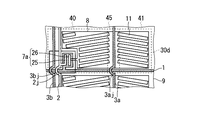
図1は、実施の形態1における液晶表示パネル90およびその液晶表示パネル90を含む液晶表示装置100の構成を模式的に示す図である。液晶表示装置100は、主要部である液晶表示パネル90等から構成される。液晶表示パネル90を構成する2枚の基板の間には液晶が封入されている。それら2枚の基板は、一方がアレイ基板10であり、他方が対向基板20である。
本実施の形態2における液晶表示パネルおよび液晶表示装置について説明する。なお、実施の形態1と同様の構成および動作については説明を省略する。
本実施の形態3における液晶表示パネルおよび液晶表示装置について説明する。なお、実施の形態1または実施の形態2と同様の構成および動作については説明を省略する。
本実施の形態4における液晶表示パネルおよび液晶表示装置について説明する。なお、実施の形態1から実施の形態3のいずれかと同様の構成および動作については説明を省略する。
Claims (7)
- 液晶を挟持して対向配置される2枚の基板のうち一方の前記基板上に、
第1方向に配列される複数の第1配線と、
第2方向に配列される複数の第2配線と、
前記第1方向に配列され、前記複数の第2配線に接続される複数の第3配線と、
前記複数の第2配線と前記複数の第3配線との交差位置に設けられ、前記複数の第2配線と前記複数の第3配線とを接続する複数のコンタクト部と、
前記複数の第1配線と前記複数の第2配線との交差位置に対応してマトリクス状に配置され表示領域を形成する複数の画素と、
前記表示領域の外側に設けられ、前記複数の第1配線の各々に接続し、各前記第1配線に接続される各前記画素が含むスイッチング素子を制御する第1ドライバICと、
前記表示領域の外側に設けられ、前記複数の第3配線の各々に接続し、各前記第3配線を介して、各前記第2配線に接続される各前記画素が含む前記スイッチング素子を制御する第2ドライバICとを備え、
各前記画素は、
下部電極と、
前記一方の基板の面内の複数の方向に延在して形成される複数のスリットを含み、前記下部電極上に絶縁膜を介して設けられる上部電極と、
前記一方の基板の前記面内に位置し、前記複数のスリットの形成方向に応じて配向分割される複数のドメインとを含み、
前記下部電極または前記上部電極のいずれか一方は、前記スイッチング素子に接続される画素電極で、他方は共通電位を印加するコモン電極であり、
各前記第3配線は、平面視において、各前記ドメイン間の境界に配線され、
各前記第3配線の一端は、各前記コンタクト部にて、各前記第2配線に接続され、
各前記第3配線の他端側は、前記第2ドライバICに接続される、液晶表示パネル。 - 前記上部電極の前記複数のスリットは、前記複数の第1配線が延伸する方向と前記複数の第2配線が延伸する方向とは異なる方向に延在し、かつ、各前記ドメイン間の前記境界に対して線対称に形成され、
前記境界は前記複数の第1配線と平行である請求項1に記載の液晶表示パネル。 - 前記複数の第2配線の本数が、前記複数の第1配線の本数よりも多く、
前記複数の第3配線の一部は、前記複数の第1配線の隣に並行して配線される請求項1または請求項2に記載の液晶表示パネル。 - 前記コモン電極に接続する少なくとも1本のコモン配線をさらに備え、
前記コモン配線は、平面視において、少なくとも1つの前記境界に配線される請求項1から請求項3のいずれか一項に記載の液晶表示パネル。 - 前記コモン配線は、前記複数の第1配線の隣に並行して配線される請求項4に記載の液晶表示パネル。
- 前記表示領域の外側に設けられ、前記複数の第1配線と前記第1ドライバICとを接続する複数の第1引き出し配線と、
前記表示領域の外側に設けられ、前記複数の第3配線と前記第2ドライバICとを接続する複数の第2引き出し配線とをさらに備え、
前記複数の第1引き出し配線の各々の一端は、前記表示領域の外形をなす一辺側にて前記複数の第1配線の各々の一端に接続し、
前記複数の第2引き出し配線の各々の一端は、前記表示領域を挟んで前記一辺に対向する他辺側にて前記複数の第3配線の各々の一端に接続する請求項1から請求項5のいずれか一項に記載の液晶表示パネル。 - 請求項1から請求項6のいずれか一項に記載の液晶表示パネルと、
前記液晶表示パネルに照明光を照射するバックライトとを備える液晶表示装置。
Priority Applications (2)
| Application Number | Priority Date | Filing Date | Title |
|---|---|---|---|
| JP2017014039A JP6745732B2 (ja) | 2017-01-30 | 2017-01-30 | 液晶表示パネルおよび液晶表示装置 |
| US15/874,235 US10622384B2 (en) | 2017-01-30 | 2018-01-18 | Liquid crystal display panel and liquid crystal display |
Applications Claiming Priority (1)
| Application Number | Priority Date | Filing Date | Title |
|---|---|---|---|
| JP2017014039A JP6745732B2 (ja) | 2017-01-30 | 2017-01-30 | 液晶表示パネルおよび液晶表示装置 |
Publications (2)
| Publication Number | Publication Date |
|---|---|
| JP2018124322A JP2018124322A (ja) | 2018-08-09 |
| JP6745732B2 true JP6745732B2 (ja) | 2020-08-26 |
Family
ID=62980478
Family Applications (1)
| Application Number | Title | Priority Date | Filing Date |
|---|---|---|---|
| JP2017014039A Active JP6745732B2 (ja) | 2017-01-30 | 2017-01-30 | 液晶表示パネルおよび液晶表示装置 |
Country Status (2)
| Country | Link |
|---|---|
| US (1) | US10622384B2 (ja) |
| JP (1) | JP6745732B2 (ja) |
Families Citing this family (9)
| Publication number | Priority date | Publication date | Assignee | Title |
|---|---|---|---|---|
| CN109064903A (zh) * | 2018-09-21 | 2018-12-21 | 武汉华星光电半导体显示技术有限公司 | 显示面板及电子装置 |
| CN109064904B (zh) * | 2018-09-21 | 2021-01-05 | 武汉天马微电子有限公司 | 一种显示面板及显示装置 |
| CN109560089B (zh) * | 2018-12-24 | 2020-11-03 | 武汉天马微电子有限公司 | 显示面板和显示装置 |
| RU2763690C1 (ru) * | 2019-11-15 | 2021-12-30 | Боэ Текнолоджи Груп Ко., Лтд. | Подложка матрицы и устройство отображения |
| CN113689796B (zh) | 2020-05-13 | 2025-03-11 | 京东方科技集团股份有限公司 | 阵列基板、其检测方法及拼接显示面板 |
| CN112068369B (zh) | 2020-09-04 | 2022-01-28 | 深圳市华星光电半导体显示技术有限公司 | 显示面板和显示装置 |
| CN114280861B (zh) * | 2020-09-27 | 2023-09-05 | 京东方科技集团股份有限公司 | 阵列基板及显示装置 |
| WO2023092299A1 (zh) * | 2021-11-23 | 2023-06-01 | 京东方科技集团股份有限公司 | 显示面板及显示装置 |
| CN116171080A (zh) * | 2023-01-19 | 2023-05-26 | 厦门天马微电子有限公司 | 显示面板及显示装置 |
Family Cites Families (9)
| Publication number | Priority date | Publication date | Assignee | Title |
|---|---|---|---|---|
| JPH08286202A (ja) | 1995-04-18 | 1996-11-01 | Toshiba Electron Eng Corp | 液晶表示装置 |
| JP3276557B2 (ja) | 1996-05-23 | 2002-04-22 | 三菱電機株式会社 | 液晶表示装置 |
| KR100471397B1 (ko) | 2001-05-31 | 2005-02-21 | 비오이 하이디스 테크놀로지 주식회사 | 프린지 필드 스위칭 액정표시장치 및 그 제조방법 |
| JP5630107B2 (ja) * | 2010-07-06 | 2014-11-26 | 富士通株式会社 | 情報検索システム、情報処理装置、及び情報検索方法 |
| JP5659708B2 (ja) * | 2010-11-08 | 2015-01-28 | 三菱電機株式会社 | 液晶表示パネル、及び液晶表示装置 |
| KR101906248B1 (ko) | 2012-12-13 | 2018-10-11 | 엘지디스플레이 주식회사 | 액정 디스플레이 장치 |
| JP2016071082A (ja) * | 2014-09-29 | 2016-05-09 | パナソニック液晶ディスプレイ株式会社 | 表示装置 |
| KR102423435B1 (ko) * | 2015-11-04 | 2022-07-21 | 삼성디스플레이 주식회사 | 액정 표시 장치 |
| CN106200184B (zh) * | 2016-09-29 | 2023-01-24 | 厦门天马微电子有限公司 | 一种显示装置、显示面板、阵列基板及其驱动方法 |
-
2017
- 2017-01-30 JP JP2017014039A patent/JP6745732B2/ja active Active
-
2018
- 2018-01-18 US US15/874,235 patent/US10622384B2/en active Active
Also Published As
| Publication number | Publication date |
|---|---|
| US10622384B2 (en) | 2020-04-14 |
| JP2018124322A (ja) | 2018-08-09 |
| US20180217431A1 (en) | 2018-08-02 |
Similar Documents
| Publication | Publication Date | Title |
|---|---|---|
| JP6745732B2 (ja) | 液晶表示パネルおよび液晶表示装置 | |
| US11796878B2 (en) | Active matrix substrate and display panel | |
| US10175818B2 (en) | Display device | |
| JP5659708B2 (ja) | 液晶表示パネル、及び液晶表示装置 | |
| US20210255514A1 (en) | Display device | |
| CN107957645A (zh) | 显示面板与其制作方法 | |
| JP5912668B2 (ja) | 液晶ディスプレイ | |
| JP4703128B2 (ja) | 液晶表示装置 | |
| US10522573B2 (en) | Display device | |
| US10845661B2 (en) | Liquid crystal display device | |
| WO2013080520A1 (ja) | 表示装置 | |
| JP2017076010A (ja) | 表示装置 | |
| KR101971143B1 (ko) | 액정표시장치 및 그 제조방법 | |
| KR20090021938A (ko) | 액정표시장치 | |
| JP7797465B2 (ja) | アレイ基板及び表示装置 | |
| KR102047744B1 (ko) | 액정표시장치용 어레이기판 | |
| JP2011128335A (ja) | 液晶装置および電子機器 | |
| JP2011048396A (ja) | 表示装置用基板及び表示装置 |
Legal Events
| Date | Code | Title | Description |
|---|---|---|---|
| A621 | Written request for application examination |
Free format text: JAPANESE INTERMEDIATE CODE: A621 Effective date: 20190712 |
|
| A977 | Report on retrieval |
Free format text: JAPANESE INTERMEDIATE CODE: A971007 Effective date: 20200417 |
|
| A131 | Notification of reasons for refusal |
Free format text: JAPANESE INTERMEDIATE CODE: A131 Effective date: 20200428 |
|
| A521 | Request for written amendment filed |
Free format text: JAPANESE INTERMEDIATE CODE: A523 Effective date: 20200618 |
|
| TRDD | Decision of grant or rejection written | ||
| A01 | Written decision to grant a patent or to grant a registration (utility model) |
Free format text: JAPANESE INTERMEDIATE CODE: A01 Effective date: 20200707 |
|
| A61 | First payment of annual fees (during grant procedure) |
Free format text: JAPANESE INTERMEDIATE CODE: A61 Effective date: 20200804 |
|
| R150 | Certificate of patent or registration of utility model |
Ref document number: 6745732 Country of ref document: JP Free format text: JAPANESE INTERMEDIATE CODE: R150 |
|
| R250 | Receipt of annual fees |
Free format text: JAPANESE INTERMEDIATE CODE: R250 |
|
| R250 | Receipt of annual fees |
Free format text: JAPANESE INTERMEDIATE CODE: R250 |
|
| R250 | Receipt of annual fees |
Free format text: JAPANESE INTERMEDIATE CODE: R250 |