JP6798521B2 - Multiplexers, high frequency front-end circuits and communication equipment - Google Patents
Multiplexers, high frequency front-end circuits and communication equipment Download PDFInfo
- Publication number
- JP6798521B2 JP6798521B2 JP2018056147A JP2018056147A JP6798521B2 JP 6798521 B2 JP6798521 B2 JP 6798521B2 JP 2018056147 A JP2018056147 A JP 2018056147A JP 2018056147 A JP2018056147 A JP 2018056147A JP 6798521 B2 JP6798521 B2 JP 6798521B2
- Authority
- JP
- Japan
- Prior art keywords
- transmission
- filter
- inductor
- terminal
- reception
- Prior art date
- Legal status (The legal status is an assumption and is not a legal conclusion. Google has not performed a legal analysis and makes no representation as to the accuracy of the status listed.)
- Active
Links
- 238000004891 communication Methods 0.000 title claims description 18
- 230000005540 biological transmission Effects 0.000 claims description 283
- 238000010897 surface acoustic wave method Methods 0.000 claims description 8
- 238000000034 method Methods 0.000 claims description 4
- 230000008569 process Effects 0.000 claims description 4
- 238000002955 isolation Methods 0.000 description 39
- 230000008878 coupling Effects 0.000 description 29
- 238000010168 coupling process Methods 0.000 description 29
- 238000005859 coupling reaction Methods 0.000 description 29
- 230000000052 comparative effect Effects 0.000 description 23
- 238000010586 diagram Methods 0.000 description 8
- 230000004048 modification Effects 0.000 description 8
- 238000012986 modification Methods 0.000 description 8
- 230000035945 sensitivity Effects 0.000 description 5
- 230000008859 change Effects 0.000 description 4
- 230000005672 electromagnetic field Effects 0.000 description 4
- 239000000758 substrate Substances 0.000 description 4
- 239000003990 capacitor Substances 0.000 description 2
- 238000006243 chemical reaction Methods 0.000 description 2
- 230000000694 effects Effects 0.000 description 2
- 230000002776 aggregation Effects 0.000 description 1
- 238000004220 aggregation Methods 0.000 description 1
- 239000000470 constituent Substances 0.000 description 1
- 230000007774 longterm Effects 0.000 description 1
- 239000000463 material Substances 0.000 description 1
- 238000003672 processing method Methods 0.000 description 1
- 230000005236 sound signal Effects 0.000 description 1
- 238000004804 winding Methods 0.000 description 1
Images


Landscapes
- Surface Acoustic Wave Elements And Circuit Networks Thereof (AREA)
- Piezo-Electric Or Mechanical Vibrators, Or Delay Or Filter Circuits (AREA)
Description
本発明は、マルチプレクサ、高周波フロントエンド回路および通信装置に関する。 The present invention relates to multiplexers, high frequency front end circuits and communication devices.
近年の携帯電話には、一端末で複数の周波数帯域および複数の無線方式、いわゆるマルチバンド化およびマルチモード化に対応することが要求されている。これに対応すべく、1つのアンテナの直下には、複数の無線搬送周波数を有する高周波信号を分波するマルチプレクサが配置される。 In recent years, mobile phones are required to support a plurality of frequency bands and a plurality of wireless systems, so-called multi-band and multi-mode, with one terminal. In order to correspond to this, a multiplexer that demultiplexes high frequency signals having a plurality of radio carrier frequencies is arranged directly under one antenna.
特許文献1には、通過帯域の異なる複数のフィルタが共通端子に接続された構成を有するマルチプレクサか開示されている。また、複数のフィルタのうちの一のフィルタと共通端子との間には、インダクタが接続されている。
マルチプレクサの性能を評価するパラメータとしてアイソレーションが挙げられる。アイソレーションを確保する構成としては、従来、フィルタ内部にインダクタンス成分を付加する構成が挙げられる。 Isolation is one of the parameters for evaluating the performance of the multiplexer. Conventionally, as a configuration for ensuring isolation, a configuration in which an inductance component is added inside the filter can be mentioned.
しかしながら、マルチプレクサに割り当てられる周波数帯域が多くなるほど、つまり、通過帯域の異なるフィルタの共通接続数が多くなるほど、アイソレーションを確保すべき周波数帯域の組み合わせが多くなる。このため、フィルタ内部に付加されるインダクタンス成分(いわゆるラダーLまたは有極Lなど)だけでは、マルチプレクサのアイソレーション特性を向上させることが困難となっている。特に、送信用のフィルタが配置された送信経路と受信用のフィルタが配置された受信経路との間において、大電力の送信信号が受信経路に漏洩すると、マルチプレクサの受信感度が低下してしまう。 However, as the frequency band allocated to the multiplexer increases, that is, as the number of common connections of filters having different pass bands increases, the number of frequency band combinations for which isolation should be ensured increases. Therefore, it is difficult to improve the isolation characteristics of the multiplexer only by the inductance component (so-called ladder L, polar L, etc.) added inside the filter. In particular, if a high-power transmission signal leaks to the reception path between the transmission path in which the transmission filter is arranged and the reception path in which the reception filter is arranged, the reception sensitivity of the multiplexer is lowered.
そこで、本発明は、上記課題を解決するためになされたものであって、共通端子に接続された送信経路と受信経路との間のアイソレーションが向上したマルチプレクサ、高周波フロントエンド回路および通信装置を提供することを目的とする。 Therefore, the present invention has been made to solve the above problems, and provides a multiplexer, a high-frequency front-end circuit, and a communication device having improved isolation between a transmission path and a reception path connected to a common terminal. The purpose is to provide.
上記目的を達成するために、本発明の一態様に係るマルチプレクサは、共通端子、第1受信端子、第1送信端子、および第2送信端子と、前記共通端子と前記第1受信端子との間に配置された第1受信フィルタと、前記共通端子と前記第1送信端子との間に配置された第1送信フィルタと、前記共通端子と前記第2送信端子との間に配置された第2送信フィルタと、前記共通端子と前記第1受信フィルタとの間に直列接続された第1インダクタと、前記第1送信端子と前記第1送信フィルタとの間に接続された第2インダクタと、前記第2送信端子と前記第2送信フィルタとの間に接続された第3インダクタと、を備え、前記第1インダクタと前記第2インダクタとは磁界結合しており、前記第1インダクタと前記第3インダクタとは磁界結合している。 In order to achieve the above object, the inductor according to one aspect of the present invention comprises a common terminal, a first receiving terminal, a first transmitting terminal, and a second transmitting terminal, and between the common terminal and the first receiving terminal. The first receiving filter arranged in the above, the first transmitting filter arranged between the common terminal and the first transmitting terminal, and the second arranged between the common terminal and the second transmitting terminal. The transmission filter, the first inductor connected in series between the common terminal and the first reception filter, the second inductor connected between the first transmission terminal and the first transmission filter, and the said. A third inductor connected between the second transmission terminal and the second transmission filter is provided, the first inductor and the second inductor are magnetically coupled, and the first inductor and the third inductor are coupled. It is magnetically coupled to the inductor.
上記構成によれば、第1送信端子から第1送信フィルタを通過した高周波送信信号のうち第1受信フィルタに漏洩する高周波成分と、第1送信端子から磁界結合した第2インダクタおよび第1インダクタを経由して第1受信フィルタに向かう高周波成分とを位相反転させることで、これら2つの高周波成分を打ち消し合うことが可能となる。また、第2送信端子から第2送信フィルタを通過した高周波送信信号のうち第1受信フィルタに漏洩する高周波成分と、第2送信端子から磁界結合した第3インダクタおよび第1インダクタを経由して第1受信フィルタに向かう高周波成分とを位相反転させることで、これら2つの高周波成分を打ち消し合うことが可能となる。つまり、送信フィルタが配置された送信経路と受信フィルタが配置された受信経路との間のアイソレーションを向上させることが可能となる。よって、相対的に電力の大きな送信信号が受信経路へ漏洩して受信感度を低下させることを抑制できる。 According to the above configuration, the high-frequency component of the high-frequency transmission signal that has passed through the first transmission filter from the first transmission terminal leaks to the first reception filter, and the second inductor and the first inductor that are magnetically coupled from the first transmission terminal. By inverting the phase of the high-frequency component that goes through the first receiving filter, these two high-frequency components can cancel each other out. Further, among the high frequency transmission signals that have passed from the second transmission terminal to the second transmission filter, the high frequency component that leaks to the first reception filter is passed through the third inductor and the first inductor that are magnetically coupled from the second transmission terminal. By inverting the phase of the high frequency component toward the 1 reception filter, these two high frequency components can cancel each other out. That is, it is possible to improve the isolation between the transmission path in which the transmission filter is arranged and the reception path in which the reception filter is arranged. Therefore, it is possible to prevent a transmission signal having a relatively large power from leaking to the reception path and lowering the reception sensitivity.
また、前記第2インダクタは、前記第1送信端子と前記第1送信フィルタとの間に直列接続され、前記第3インダクタは、前記第2送信端子と前記第2送信フィルタとの間に直列接続され、前記第1インダクタのインダクタンス値は、前記第2インダクタのインダクタンス値よりも大きく、かつ、前記第3インダクタのインダクタンス値よりも大きくてもよい。 Further, the second inductor is connected in series between the first transmission terminal and the first transmission filter, and the third inductor is connected in series between the second transmission terminal and the second transmission filter. The inductance value of the first inductor may be larger than the inductance value of the second inductor and may be larger than the inductance value of the third inductor.
信号経路にインダクタが直列接続された場合、当該インダクタのインダクタンス値が大きいほど、高周波信号の伝搬損失が大きくなる。特に大電力を送信する必要がある送信経路において、高周波信号の伝搬ロスを極力低減することがマルチプレクサの性能向上にとって重要となる。 When an inductor is connected in series to the signal path, the larger the inductance value of the inductor, the larger the propagation loss of the high frequency signal. Especially in the transmission path where a large amount of power needs to be transmitted, it is important to reduce the propagation loss of the high frequency signal as much as possible in order to improve the performance of the multiplexer.
上記構成によれば、送信経路に直列接続された第2インダクタおよび第3インダクタは、受信経路に直列接続された第1インダクタよりもインダクタンス値が小さいので、第1インダクタと第2インダクタとの磁界結合、および、第1インダクタと第3インダクタとの磁界結合を確保しつつ、高周波送信信号の伝搬損失を低減できる。よって、マルチプレクサの高周波伝搬性能を向上させることが可能となる。 According to the above configuration, the second inductor and the third inductor connected in series with the transmission path have a smaller inductance value than the first inductor connected in series with the reception path, so that the magnetic field between the first inductor and the second inductor It is possible to reduce the propagation loss of the high frequency transmission signal while ensuring the coupling and the magnetic field coupling between the first inductor and the third inductor. Therefore, it is possible to improve the high frequency propagation performance of the multiplexer.
また、前記第1受信フィルタは、第1周波数帯域に割り当てられた第1送信帯域および第1受信帯域のうちの前記第1受信帯域を通過帯域とし、前記第1送信フィルタは、前記第1送信帯域を通過帯域とし、前記第2送信フィルタは、前記第1周波数帯域と異なる第2周波数帯域に割り当てられた第2送信帯域および第2受信帯域のうちの前記第2送信帯域を通過帯域としてもよい。 Further, the first reception filter has the first reception band of the first transmission band and the first reception band assigned to the first frequency band as a pass band, and the first transmission filter is the first transmission. The band is used as a pass band, and the second transmission filter may use the second transmission band of the second transmission band and the second reception band assigned to the second frequency band different from the first frequency band as the pass band. Good.
上記構成によれば、第1送信フィルタを通過した高周波送信信号のうち第1受信フィルタに漏洩する高周波成分と、第1送信端子から磁界結合した第2インダクタおよび第1インダクタを経由して第1受信フィルタに向かう高周波成分とを位相反転させることで、これら2つの高周波成分を打ち消し合うことが可能となる。よって、第1周波数帯域の送信信号および受信信号の間のアイソレーションを向上させることが可能となる。 According to the above configuration, the high frequency component of the high frequency transmission signal that has passed through the first transmission filter leaks to the first reception filter, and the first inductor passes through the second inductor and the first inductor that are magnetically coupled from the first transmission terminal. By inverting the phase of the high frequency component toward the receiving filter, these two high frequency components can cancel each other out. Therefore, it is possible to improve the isolation between the transmission signal and the reception signal in the first frequency band.
また、第2送信フィルタを通過した高周波送信信号のうち第1受信フィルタに漏洩する高周波成分と、第2送信端子から磁界結合した第3インダクタおよび第1インダクタを経由して第1受信フィルタに向かう高周波成分とを位相反転させることで、これら2つの高周波成分を打ち消し合うことが可能となる。よって、第1周波数帯域の受信信号および第2周波数帯域の送信信号の間のクロスアイソレーションを向上させることが可能となる。 Further, among the high-frequency transmission signals that have passed through the second transmission filter, the high-frequency component leaking to the first reception filter goes to the first reception filter via the third inductor and the first inductor that are magnetically coupled from the second transmission terminal. By inverting the phase with the high frequency component, these two high frequency components can cancel each other out. Therefore, it is possible to improve the cross isolation between the received signal in the first frequency band and the transmitted signal in the second frequency band.
また、前記第1受信フィルタ、前記第1送信フィルタ、および前記第2送信フィルタは、弾性表面波フィルタ、BAW(Bulk Acoustic Wave)を用いた弾性波フィルタ、LC共振フィルタ、および誘電体フィルタのいずれかであってもよい。 The first receiving filter, the first transmitting filter, and the second transmitting filter are any of a surface acoustic wave filter, a surface acoustic wave filter using BAW (Bulk Acoustic Wave), an LC resonance filter, and a dielectric filter. It may be.
これにより、第1受信フィルタ、第1送信フィルタ、および第2送信フィルタを小型化できるので、マルチプレクサの小型化および低価格化が可能となる。 As a result, the first reception filter, the first transmission filter, and the second transmission filter can be miniaturized, so that the multiplexer can be miniaturized and the price can be reduced.
また、本発明の一態様に係るマルチプレクサは、共通端子、第1送信端子、第1受信端子、および第2受信端子と、前記共通端子と前記第1送信端子との間に配置された第1送信フィルタと、前記共通端子と前記第1受信端子との間に配置された第1受信フィルタと、前記共通端子と前記第2受信端子との間に配置された第2受信フィルタと、前記共通端子と前記第1送信フィルタとの間に直列接続された第1インダクタと、前記第1受信端子と前記第1受信フィルタとの間に接続された第2インダクタと、前記第2受信端子と前記第2受信フィルタとの間に接続された第3インダクタと、を備え、前記第1インダクタと前記第2インダクタとは磁界結合しており、前記第1インダクタと前記第3インダクタとは磁界結合している。 Further, the multiplexer according to one aspect of the present invention is a first one arranged between a common terminal, a first transmitting terminal, a first receiving terminal, and a second receiving terminal, and the common terminal and the first transmitting terminal. The transmission filter, the first reception filter arranged between the common terminal and the first reception terminal, the second reception filter arranged between the common terminal and the second reception terminal, and the common The first inductor connected in series between the terminal and the first transmitting filter, the second inductor connected between the first receiving terminal and the first receiving filter, the second receiving terminal and the said. A third inductor connected to the second receiving filter is provided, the first inductor and the second inductor are magnetically coupled, and the first inductor and the third inductor are magnetically coupled. ing.
上記構成によれば、第1送信端子から第1送信フィルタを通過した高周波送信信号のうち第1受信フィルタに漏洩する高周波成分と、第1送信端子から磁界結合した第1インダクタおよび第2インダクタを経由して第1受信端子に向かう高周波成分とを位相反転させることで、これら2つの高周波成分を打ち消し合うことが可能となる。また、第1送信端子から第1送信フィルタを通過した高周波送信信号のうち第2受信フィルタに漏洩する高周波成分と、第1送信端子から磁界結合した第1インダクタおよび第3インダクタを経由して第2受信端子に向かう高周波成分とを位相反転させることで、これら2つの高周波成分を打ち消し合うことが可能となる。つまり、送信フィルタが配置された送信経路と受信フィルタが配置された受信経路との間のアイソレーションを向上させることが可能となる。よって、相対的に電力の大きな送信信号が受信経路へ漏洩して受信感度を低下させることを抑制できる。 According to the above configuration, the high frequency component leaking from the first transmission terminal to the first reception filter among the high frequency transmission signals that have passed through the first transmission filter, and the first inductor and the second inductor magnetically coupled from the first transmission terminal are separated. By inverting the phase of the high-frequency component that goes to the first receiving terminal via the route, these two high-frequency components can cancel each other out. Further, among the high frequency transmission signals that have passed from the first transmission terminal to the first transmission filter, the high frequency component leaking to the second reception filter is passed through the first inductor and the third inductor that are magnetically coupled from the first transmission terminal. By inverting the phase of the high frequency component toward the two receiving terminals, these two high frequency components can cancel each other out. That is, it is possible to improve the isolation between the transmission path in which the transmission filter is arranged and the reception path in which the reception filter is arranged. Therefore, it is possible to prevent a transmission signal having a relatively large power from leaking to the reception path and lowering the reception sensitivity.
また、前記第2インダクタは、前記第1受信端子と前記第1受信フィルタとの間に直列接続され、前記第3インダクタは、前記第2受信端子と前記第2受信フィルタとの間に直列接続され、前記第1インダクタのインダクタンス値は、前記第2インダクタのインダクタンス値よりも小さく、かつ、前記第3インダクタのインダクタンス値よりも小さくてもよい。 Further, the second inductor is connected in series between the first receiving terminal and the first receiving filter, and the third inductor is connected in series between the second receiving terminal and the second receiving filter. The inductance value of the first inductor may be smaller than the inductance value of the second inductor and smaller than the inductance value of the third inductor.
これにより、送信経路に直列接続された第1インダクタは、受信経路に直列接続された第2インダクタおよび第3インダクタよりもインダクタンス値が小さいので、第1インダクタと第2インダクタとの磁界結合、および、第1インダクタと第3インダクタとの磁界結合を確保しつつ、高周波送信信号の伝搬損失を低減できる。よって、マルチプレクサの高周波伝搬性能を向上させることが可能となる。 As a result, the first inductor connected in series with the transmission path has a smaller inductance value than the second inductor and the third inductor connected in series with the reception path, so that the magnetic field coupling between the first inductor and the second inductor and the magnetic field coupling and , The propagation loss of the high frequency transmission signal can be reduced while ensuring the magnetic field coupling between the first inductor and the third inductor. Therefore, it is possible to improve the high frequency propagation performance of the multiplexer.
また、前記第1送信フィルタは、第1周波数帯域に割り当てられた第1送信帯域および第1受信帯域のうちの前記第1送信帯域を通過帯域とし、前記第1受信フィルタは、前記第1受信帯域を通過帯域とし、前記第2受信フィルタは、前記第1周波数帯域と異なる第2周波数帯域に割り当てられた第2送信帯域および第2受信帯域のうちの前記第2受信帯域を通過帯域としてもよい。 Further, the first transmission filter uses the first transmission band of the first transmission band and the first reception band assigned to the first frequency band as a pass band, and the first reception filter uses the first reception band. The band is used as a pass band, and the second reception filter may use the second reception band of the second transmission band and the second reception band assigned to the second frequency band different from the first frequency band as the pass band. Good.
上記構成によれば、第1送信フィルタを通過した高周波送信信号のうち第1受信フィルタに漏洩する高周波成分と、第1送信端子から磁界結合した第1インダクタおよび第2インダクタを経由して第1受信端子に向かう高周波成分とを位相反転させることで、これら2つの高周波成分を打ち消し合うことが可能となる。よって、第1周波数帯域の送信信号および受信信号の間のアイソレーションを向上させることが可能となる。 According to the above configuration, the high-frequency component of the high-frequency transmission signal that has passed through the first transmission filter leaks to the first reception filter, and the first inductor that is magnetically coupled from the first transmission terminal via the first inductor and the second inductor. By inverting the phase of the high frequency component toward the receiving terminal, these two high frequency components can cancel each other out. Therefore, it is possible to improve the isolation between the transmission signal and the reception signal in the first frequency band.
また、第1送信フィルタを通過した高周波送信信号のうち第2受信フィルタに漏洩する高周波成分と、第1送信端子から磁界結合した第1インダクタおよび第3インダクタを経由して第2受信端子に向かう高周波成分とを位相反転させることで、これら2つの高周波成分を打ち消し合うことが可能となる。よって、第2周波数帯域の受信信号および第1周波数帯域の送信信号の間のクロスアイソレーションを向上させることが可能となる。 Further, the high-frequency component of the high-frequency transmission signal that has passed through the first transmission filter that leaks to the second reception filter goes to the second reception terminal via the first inductor and the third inductor that are magnetically coupled from the first transmission terminal. By inverting the phase with the high frequency component, these two high frequency components can cancel each other out. Therefore, it is possible to improve the cross isolation between the received signal in the second frequency band and the transmitted signal in the first frequency band.
また、前記第1送信フィルタ、前記第1受信フィルタ、および前記第2受信フィルタは、弾性表面波フィルタ、BAWを用いた弾性波フィルタ、LC共振フィルタ、および誘電体フィルタのいずれかであってもよい。 Further, the first transmission filter, the first reception filter, and the second reception filter may be any of a surface acoustic wave filter, a surface acoustic wave filter using BAW, an LC resonance filter, and a dielectric filter. Good.
これにより、第1送信フィルタ、第1受信フィルタ、および第2受信フィルタを小型化できるので、マルチプレクサの小型化および低価格化が可能となる。 As a result, the first transmission filter, the first reception filter, and the second reception filter can be miniaturized, so that the multiplexer can be miniaturized and the price can be reduced.
また、さらに、アンテナ素子に接続されるアンテナ端子と、前記アンテナ端子と前記共通端子との間に接続されたインピーダンス整合回路と、を備えてもよい。 Further, an antenna terminal connected to the antenna element and an impedance matching circuit connected between the antenna terminal and the common terminal may be provided.
これにより、第1インダクタ、第2インダクタ、および第3インダクタのインダクタンス値を、磁界結合の結合度を優先して調整しても、上記インピーダンス整合回路により各送信経路および各受信経路間のインピーダンス整合を最適化できる。よって、第1インダクタ、第2インダクタ、および第3インダクタのインダクタンス値の設定自由度が向上する。 As a result, even if the inductance values of the first inductor, the second inductor, and the third inductor are adjusted with priority given to the degree of coupling of the magnetic field coupling, the impedance matching circuit matches the impedance between each transmission path and each reception path. Can be optimized. Therefore, the degree of freedom in setting the inductance values of the first inductor, the second inductor, and the third inductor is improved.
また、本発明の一態様に係る高周波フロントエンド回路は、上記いずれかに記載のマルチプレクサと、前記マルチプレクサに接続された増幅回路と、を備える。 Further, the high frequency front-end circuit according to one aspect of the present invention includes the multiplexer described in any of the above and an amplifier circuit connected to the multiplexer.
これにより、送信フィルタが配置された送信経路と受信フィルタが配置された受信経路との間のアイソレーションが向上した高周波フロントエンド回路を提供できる。 This makes it possible to provide a high-frequency front-end circuit in which the isolation between the transmission path in which the transmission filter is arranged and the reception path in which the reception filter is arranged is improved.
また、本発明の一態様に係る通信装置は、アンテナ素子で送受信される高周波信号を処理するRF信号処理回路と、前記アンテナ素子と前記RF信号処理回路との間で前記高周波信号を伝達する上記記載の高周波フロントエンド回路と、を備える。 Further, the communication device according to one aspect of the present invention is the above-mentioned RF signal processing circuit that processes high-frequency signals transmitted and received by the antenna element, and the high-frequency signal that is transmitted between the antenna element and the RF signal processing circuit. It comprises the high frequency front end circuit described.
これにより、送信フィルタが配置された送信経路と受信フィルタが配置された受信経路との間のアイソレーションが向上した通信装置を提供できる。 Thereby, it is possible to provide a communication device having improved isolation between the transmission path in which the transmission filter is arranged and the reception path in which the reception filter is arranged.
本発明に係るマルチプレクサ、高周波フロントエンド回路および通信装置によれば、共通端子に接続された送信経路と受信経路との間のアイソレーションを向上させることが可能となる。 According to the multiplexer, high frequency front-end circuit and communication device according to the present invention, it is possible to improve the isolation between the transmission path and the reception path connected to the common terminal.
以下、本発明の実施の形態について、図面を用いて詳細に説明する。なお、以下で説明する実施の形態は、いずれも包括的または具体的な例を示すものである。以下の実施の形態で示される数値、形状、材料、構成要素、構成要素の配置および接続形態などは、一例であり、本発明を限定する主旨ではない。以下の実施の形態における構成要素のうち、独立請求項に記載されていない構成要素については、任意の構成要素として説明される。また、図面に示される構成要素の大きさ、または大きさの比は、必ずしも厳密ではない。また、各図において、実質的に同一の構成に対しては同一の符号を付しており、重複する説明は省略または簡略化する場合がある。また、以下の実施の形態において、「接続される」とは、直接接続される場合だけでなく、他の素子等を介して電気的に接続される場合も含まれる。 Hereinafter, embodiments of the present invention will be described in detail with reference to the drawings. It should be noted that all of the embodiments described below are comprehensive or specific examples. Numerical values, shapes, materials, components, arrangement of components, connection modes, etc. shown in the following embodiments are examples, and are not intended to limit the present invention. Among the components in the following embodiments, the components not described in the independent claims are described as arbitrary components. Also, the sizes of the components shown in the drawings, or the ratio of sizes, are not always exact. Further, in each figure, substantially the same configuration is designated by the same reference numerals, and duplicate description may be omitted or simplified. Further, in the following embodiments, "connected" includes not only the case of being directly connected but also the case of being electrically connected via another element or the like.
また、以下の実施の形態において、「インダクタAとインダクタBとが磁界結合する」とは、「インダクタAとインダクタBとが、磁界を遮断するシールド部材を介在せずに配置された状態で、磁界結合している」ことと定義される。 Further, in the following embodiment, "the inductor A and the inductor B are magnetically coupled" means that "the inductor A and the inductor B are arranged without a shield member that blocks the magnetic field." It is defined as "magnetic field coupled".
(実施の形態1)
[1.マルチプレクサ1Aの基本構成]
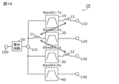
図1Aは、実施の形態1に係るマルチプレクサ1Aの回路構成図である。同図に示すように、マルチプレクサ1Aは、送信フィルタ10および30と、受信フィルタ20および40と、インダクタ12、21および32と、アンテナ端子100と、共通端子101と、送信端子110および130と、受信端子120および140と、整合回路50と、を備える。
(Embodiment 1)
[1. Basic configuration of
FIG. 1A is a circuit configuration diagram of the
アンテナ端子100は、アンテナ素子に接続される接続端子である。
The
共通端子101は、送信フィルタ10および30、インダクタ21、ならびに受信フィルタ40と接続されており、また、整合回路50を介してアンテナ端子100に接続されている。
The
送信端子110は、高周波送信信号を増幅するパワーアンプ回路に接続される第1送信端子である。送信端子130は、高周波送信信号を増幅するパワーアンプ回路に接続される第2送信端子である。
The
受信端子120は、高周波受信信号を増幅するローノイズアンプ回路に接続される第1受信端子である。
The
受信端子140は、高周波受信信号を増幅するローノイズアンプ回路に接続される受信端子である。
The
送信フィルタ10は、共通端子101と送信端子110との間に配置され、送信回路(RFICなど)で生成された高周波送信信号を、送信端子110を経由して入力し、当該高周波送信信号をBandA1の送信通過帯域でフィルタリングして共通端子101へ出力する第1送信フィルタである。
The
受信フィルタ20は、共通端子101と受信端子120との間に配置され、共通端子101から入力された高周波受信信号を入力し、当該高周波受信信号をBandA2の受信通過帯域でフィルタリングして受信端子120へ出力する第1受信フィルタである。
The
送信フィルタ30は、共通端子101と送信端子130との間に配置され、送信回路(RFICなど)で生成された高周波送信信号を、送信端子130を経由して入力し、当該高周波送信信号をBandA3の送信通過帯域でフィルタリングして共通端子101へ出力する第2送信フィルタである。
The
受信フィルタ40は、共通端子101と受信端子140との間に配置され、共通端子101から入力された高周波受信信号を入力し、当該高周波受信信号をBandA4の受信通過帯域でフィルタリングして受信端子140へ出力する。
The
インダクタ12は、送信端子110と送信フィルタ10との間に接続された第2インダクタである。
The
インダクタ32は、送信端子130と送信フィルタ30との間に接続された第3インダクタである。
The
インダクタ21は、共通端子101と受信フィルタ20との間に直列接続された第1インダクタである。
The
整合回路50は、アンテナ端子100と共通端子101との間に接続され、アンテナ素子とマルチプレクサ1Aとのインピーダンスを整合するインピーダンス整合回路である。整合回路50は、例えば、アンテナ端子100および共通端子101に直列接続された1つのインダクタで構成されていてもよいし、また、アンテナ端子100と共通端子101との接続ノードとグランドとの間に接続された1つのインダクタであってもよい。さらに、これらのインダクタのほか、キャパシタが直列または並列に接続されていてもよい。つまり、整合回路50は、1以上のインダクタおよび1以上のキャパシタのそれぞれが、直列または並列に接続された回路構成を有していればよい。
The matching
上記回路構成を有するマルチプレクサ1Aにおいて、インダクタ21とインダクタ12とは磁界結合しており、かつ、インダクタ21とインダクタ32とは磁界結合している。
In the
これによれば、送信端子110から送信フィルタ10を通過した高周波送信信号のうち受信フィルタ20に漏洩する高周波成分と、送信端子110から磁界結合したインダクタ12および21を経由して受信フィルタ20に向かう高周波成分とを打ち消し合うことが可能となる。
According to this, the high-frequency component of the high-frequency transmission signal that has passed through the
なお、上記2つの高周波成分が位相反転した関係となるようにインダクタ12および21の電磁界結合度を最適化し、送信端子110から送信フィルタ10を通過した高周波送信信号のうち受信フィルタ20に漏洩する高周波成分を最小化することが好ましい。
The electromagnetic field coupling of the
また、送信端子130から送信フィルタ30を通過した高周波送信信号のうち受信フィルタ20に漏洩する高周波成分と、送信端子130から磁界結合したインダクタ32および21を経由して受信フィルタ20に向かう高周波成分とを打ち消し合うことが可能となる。
Further, among the high-frequency transmission signals that have passed from the
なお、上記2つの高周波成分が位相反転した関係となるようにインダクタ32および21の電磁界結合度を最適化し、送信端子130から送信フィルタ30を通過した高周波送信信号のうち受信フィルタ20に漏洩する高周波成分を最小化することが好ましい。
The electromagnetic field coupling of the
つまり、送信フィルタ10および30が配置された送信経路と、受信フィルタ20が配置された受信経路との間のアイソレーションを向上させることが可能となる。よって、相対的に電力の大きな高周波送信信号が受信経路へ漏洩してマルチプレクサ1Aの受信感度を低下させることを抑制できる。
That is, it is possible to improve the isolation between the transmission path in which the transmission filters 10 and 30 are arranged and the reception path in which the
また、整合回路50が配置されることにより、インダクタ12、21および32のインダクタンス値を、磁界結合の結合度を優先して調整しても、アンテナ素子、各送信経路および各受信経路の間のインピーダンス整合を最適化できる。よって、インダクタ12、21および32のインダクタンス値の設定自由度が向上する。
Further, by arranging the matching
なお、整合回路50は、必須の構成要素ではなく、なくてもよい。
The matching
また、本実施の形態に係るマルチプレクサ1Aにおいて、BandA1とBandA2とは、同じ周波数帯域であってもよいし、また、異なる周波数帯域であってもよい。BandA1とBandA2とが同じ周波数帯域である場合には、送信フィルタ10と受信フィルタ20とは、例えば、当該周波数帯域に送信通過帯域および受信通過帯域が割り当てられたデュプレクサを構成する。また、BandA1とBandA2とが異なる周波数帯域である場合には、送信フィルタ10および受信フィルタ20は、それぞれ、異なる通過帯域を有する単体フィルタを構成する。同様に、BandA3とBandA4とは、同じ周波数帯域であってもよいし、また、異なる周波数帯域であってもよい。BandA3とBandA4とが同じ周波数帯域である場合には、送信フィルタ30と受信フィルタ40とは、例えば、当該周波数帯域に送信通過帯域および受信通過帯域が割り当てられたデュプレクサを構成する。また、BandA3とBandA4とが異なる周波数帯域である場合には、送信フィルタ30および受信フィルタ40は、それぞれ、異なる通過帯域を有する単体フィルタを構成する。
Further, in the
また、送信フィルタ10および30、ならびに、受信フィルタ20および40は、弾性表面波フィルタ、BAW(Bulk Acoustic Wave)を用いた弾性波フィルタ、LC共振フィルタ、および誘電体フィルタのいずれかである。これにより、各フィルタを小型化できるので、マルチプレクサ1Aの小型化および低価格化が可能となる。
Further, the transmission filters 10 and 30 and the reception filters 20 and 40 are any of an elastic surface wave filter, an elastic wave filter using a BAW (Bulk Acoustic Wave), an LC resonance filter, and a dielectric filter. As a result, each filter can be miniaturized, so that the
なお、送信フィルタ10および30、ならびに、受信フィルタ20は、弾性波フィルタであることが好ましい。特に、送信フィルタ10および30、ならびに、受信フィルタ20は、1以上の直列腕共振子および1以上の並列腕共振子からなるラダー型の弾性波フィルタであってもよい。この場合、インダクタ21、12および32は、フィルタ通過特性の減衰極を調整する機能およびインピーダンス整合機能を有することが可能となる。
It is preferable that the transmission filters 10 and 30 and the
[2.変形例に係るマルチプレクサの構成]
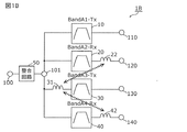
図1Bは、実施の形態1の変形例に係るマルチプレクサ1Bの回路構成図である。本変形例に係るマルチプレクサ1Bは、2送信経路および1受信経路にインダクタが配置されている実施の形態1に係るマルチプレクサ1Aと比較して、1送信経路および2受信経路にインダクタが配置されている点が構成として異なる。以下、本変形例に係るマルチプレクサ1Bについて、実施の形態1に係るマルチプレクサ1Aと同じ点は説明を省略し、異なる点を中心に説明する。
[2. Configuration of multiplexer according to modified example]
FIG. 1B is a circuit configuration diagram of a
図1Bに示すように、マルチプレクサ1Bは、送信フィルタ10および30と、受信フィルタ20および40と、インダクタ22、31および42と、アンテナ端子100と、共通端子101と、送信端子110および130と、受信端子120および140と、整合回路50と、を備える。
As shown in FIG. 1B, the
共通端子101は、送信フィルタ10、受信フィルタ20および40、ならびにインダクタ31と接続されており、また、整合回路50を介してアンテナ端子100に接続されている。
The
送信端子110は、高周波送信信号を増幅するパワーアンプ回路に接続される送信端子である。送信端子130は、高周波送信信号を増幅するパワーアンプ回路に接続される第1送信端子である。
The
受信端子120は、高周波受信信号を増幅するローノイズアンプ回路に接続される第2受信端子である。
The
受信端子140は、高周波受信信号を増幅するローノイズアンプ回路に接続される第1受信端子である。
The
インダクタ22は、受信端子120と受信フィルタ20との間に接続された第3インダクタである。
The
インダクタ42は、受信端子140と受信フィルタ40との間に接続された第2インダクタである。
The
インダクタ31は、共通端子101と送信フィルタ30との間に直列接続された第1インダクタである。
The
上記回路構成を有するマルチプレクサ1Bにおいて、インダクタ31とインダクタ22とは磁界結合しており、かつ、インダクタ31とインダクタ42とは磁界結合している。
In the
これによれば、送信端子130から送信フィルタ30を通過した高周波送信信号のうち受信フィルタ40に漏洩する高周波成分と、送信端子130から磁界結合したインダクタ31および42を経由して受信端子140に向かう高周波成分とを打ち消し合うことが可能となる。
According to this, among the high-frequency transmission signals that have passed through the
なお、上記2つの高周波成分が位相反転した関係となるようにインダクタ31および42の電磁界結合度を最適化し、送信端子130から送信フィルタ30を通過した高周波送信信号のうち受信フィルタ40に漏洩する高周波成分を最小化することが好ましい。
The electromagnetic field coupling of the
また、送信端子130から送信フィルタ30を通過した高周波送信信号のうち受信フィルタ20に漏洩する高周波成分と、送信端子130から磁界結合したインダクタ31および22を経由して受信端子120に向かう高周波成分とを打ち消し合うことが可能となる。
Further, among the high-frequency transmission signals that have passed through the
なお、上記2つの高周波成分が位相反転した関係となるようにインダクタ31および22の電磁界結合度を最適化し、送信端子130から送信フィルタ30を通過した高周波送信信号のうち受信フィルタ20に漏洩する高周波成分を最小化することが好ましい。
The electromagnetic field coupling of the
つまり、送信フィルタ30が配置された送信経路と受信フィルタ20および40が配置された受信経路との間のアイソレーションを向上させることが可能となる。よって、相対的に電力の大きな送信信号が受信経路へ漏洩して受信感度を低下させることを抑制できる。
That is, it is possible to improve the isolation between the transmission path in which the
また、本変形例に係るマルチプレクサ1Bにおいて、BandA1とBandA2とは、同じ周波数帯域であってもよいし、また、異なる周波数帯域であってもよい。BandA1とBandA2とが同じ周波数帯域である場合には、送信フィルタ10と受信フィルタ20とは、例えば、当該周波数帯域に送信通過帯域および受信通過帯域が割り当てられたデュプレクサを構成する。また、BandA1とBandA2とが異なる周波数帯域である場合には、送信フィルタ10および受信フィルタ20は、それぞれ、異なる通過帯域を有する単体フィルタを構成する。同様に、BandA3とBandA4とは、同じ周波数帯域であってもよいし、また、異なる周波数帯域であってもよい。BandA3とBandA4とが同じ周波数帯域である場合には、送信フィルタ30と受信フィルタ40とは、例えば、当該周波数帯域に送信通過帯域および受信通過帯域が割り当てられたデュプレクサを構成する。また、BandA3とBandA4とが異なる周波数帯域である場合には、送信フィルタ30および受信フィルタ40は、それぞれ、異なる通過帯域を有する単体フィルタを構成する。
Further, in the
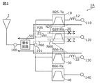
[3.実施例に係るマルチプレクサ1Aの構成]
図2は、実施例に係るマルチプレクサ1Aの回路構成図である。本実施例に係るマルチプレクサ1Aは、実施の形態1に係るマルチプレクサ1Aを、LTE(Long Term Evolution)のBand25および66のクワッドプレクサに適用した例である。
[3. Configuration of
FIG. 2 is a circuit configuration diagram of the
送信フィルタ10は、Band25(第1周波数帯域)の送信通過帯域(1850−1915MHz:第1送信帯域)を通過帯域とする帯域通過型フィルタである。
The
受信フィルタ20は、Band25(第1周波数帯域)の受信通過帯域(1930−1995MHz:第1受信帯域)を通過帯域とする帯域通過型フィルタである。
The
送信フィルタ30は、Band66(第2周波数帯域)の送信通過帯域(1710−1780MHz:第2送信帯域)を通過帯域とする帯域通過型フィルタである。
The
受信フィルタ40は、Band66(第2周波数帯域)の受信通過帯域(2110−2200MHz:第2受信帯域)を通過帯域とする帯域通過型フィルタである。
The
インダクタ12は、送信端子110と送信フィルタ10との間に直列接続されている。
The
インダクタ32は、送信端子130と送信フィルタ30との間に直列接続されている。
The
インダクタ21は、共通端子101と受信フィルタ20との間に直列接続されている。
The
本実施例において、Band25の高周波送信信号が、受信フィルタ20が配置されたBand25の受信経路へと漏洩してしまうとともに、Band66の高周波送信信号が、共通端子101を経由してBand25の受信経路へと漏洩してしまう可能性がある。
In this embodiment, the high frequency transmission signal of the Band 25 leaks to the reception path of the Band 25 in which the
これに対して、実施例に係るマルチプレクサ1Aでは、インダクタ21とインダクタ12とが磁界結合しており、かつ、インダクタ21とインダクタ32とが磁界結合している。
On the other hand, in the
これによれば、送信フィルタ10を通過した高周波送信信号のうち受信フィルタ20に漏洩する高周波成分P25と、送信端子110から磁界結合したインダクタ12および21を経由して受信フィルタ20に向かう高周波成分N25とを位相反転させることで、これら2つの高周波成分を打ち消し合うことが可能となる。よって、Band25の送信信号および受信信号の間のアイソレーションを向上させることが可能となる。
According to this, the high-frequency component P25 leaking to the
また、送信フィルタ30を通過した高周波送信信号のうち受信フィルタ20に漏洩する高周波成分P66と、送信端子130から磁界結合したインダクタ32および21を経由して受信フィルタ20に向かう高周波成分N66とを位相反転させることで、これら2つの高周波成分を打ち消し合うことが可能となる。よって、異なる周波数帯域の受信信号および送信信号の間のクロスアイソレーションを向上させることが可能となる。
Further, the phase of the high frequency component P66 leaking to the
また、本実施例に係るマルチプレクサ1Aでは、インダクタ21のインダクタンス値を5.2nH、インダクタ12のインダクタンス値を1.5nH、インダクタ32のインダクタンス値を3.9nHとしている。つまり、インダクタ21のインダクタンス値は、インダクタ12のインダクタンス値よりも大きく、かつ、インダクタ32のインダクタンス値よりも大きい。
Further, in the
信号経路にインダクタが直列接続された場合、当該インダクタのインダクタンス値が大きいほど、高周波信号の伝搬損失が大きくなる。特に大電力を送信する必要がある送信経路において、高周波信号の伝搬ロスを極力低減することがマルチプレクサ1Aの性能向上にとって重要となる。
When an inductor is connected in series to the signal path, the larger the inductance value of the inductor, the larger the propagation loss of the high frequency signal. In particular, in a transmission path where a large amount of power needs to be transmitted, it is important to reduce the propagation loss of high-frequency signals as much as possible in order to improve the performance of the
インダクタ12、21、および32の上記関係によれば、送信フィルタ10が配置された送信経路および送信フィルタ30が配置された送信経路に直列接続されたインダクタ12および32は、受信フィルタ20が配置された受信経路に直列接続されたインダクタ21よりもインダクタンス値が小さい。よって、インダクタ21とインダクタ12との磁界結合、および、インダクタ21とインダクタ32との磁界結合を確保しつつ、高周波送信信号の伝搬損失を低減できる。よって、マルチプレクサ1Aの高周波伝搬性能を向上させることが可能となる。
According to the above relationship of the
なお、送信経路における信号伝搬ロスを極力低減するという観点から、変形例に係るマルチプレクサ1Bでは、インダクタ31のインダクタンス値は、インダクタ22のインダクタンス値よりも小さく、かつ、インダクタ42のインダクタンス値よりも小さいことが好ましい。これにより、インダクタ31とインダクタ32との磁界結合、および、インダクタ31とインダクタ42との磁界結合を確保しつつ、高周波送信信号の伝搬損失を低減できる。よって、マルチプレクサ1Bの高周波伝搬性能を向上させることが可能となる。
From the viewpoint of reducing the signal propagation loss in the transmission path as much as possible, in the
なお、インダクタ12、21、および32は、例えば、送信フィルタ10および30、ならびに、受信フィルタ20および40が実装された実装基板上に配置されたチップ状のインダクタンス素子であってもよい。この場合、インダクタ12とインダクタ21との磁界結合度、および、インダクタ12とインダクタ32との磁界結合度は、チップ状のインダクタ12とインダクタ21との間隔および配置方向、ならびに、チップ状のインダクタ32とインダクタ21との間隔および配置方向により調整される。
The
また、インダクタ12、21、および32は、少なくとも1つが、実装基板内に内蔵されたインダクタンス素子であってもよい。この場合、実装基板内に内蔵されたインダクタンス素子は、例えば、実装基板内に積層されたコイルパターンにより構成される。この場合、インダクタ12とインダクタ21との磁界結合度、および、インダクタ12とインダクタ32との磁界結合度は、基板内蔵されたインダクタ12とインダクタ21との間隔および配置関係、ならびに、チップ状のインダクタ32とインダクタ21との間隔および配置関係により調整される。なお、基板内蔵された2つのインダクタの配置関係とは、コールパターンの巻回軸を重ねる、または、離間させるなどが挙げられる。
Further, at least one of the
なお、変形例に係るマルチプレクサ1Bにおいても、LTEのBand25および66のクワッドプレクサに適用することが可能である。以下、変形例に係るマルチプレクサ1BをLTEのBand25および66のクワッドプレクサに適用した例を示す。
The
送信フィルタ10は、Band25(第2周波数帯域)の送信通過帯域(1850−1915MHz:第2送信帯域)を通過帯域とする帯域通過型フィルタである。
The
受信フィルタ20は、Band25(第2周波数帯域)の受信通過帯域(1930−1995MHz:第2受信帯域)を通過帯域とする帯域通過型フィルタである。
The
送信フィルタ30は、Band66(第1周波数帯域)の送信通過帯域(1710−1780MHz:第1送信帯域)を通過帯域とする帯域通過型フィルタである。
The
受信フィルタ40は、Band66(第1周波数帯域)の受信通過帯域(2110−2200MHz:第1受信帯域)を通過帯域とする帯域通過型フィルタである。
The
インダクタ22は、受信端子120と受信フィルタ20との間に直列接続されている。
The
インダクタ42は、受信端子140と受信フィルタ40との間に直列接続されている。
The
インダクタ31は、共通端子101と送信フィルタ30との間に直列接続されている。
The
本実施例において、Band66の高周波送信信号が、受信フィルタ40が配置されたBand66の受信経路へと漏洩してしまうとともに、共通端子101を経由してBand25の受信経路へと漏洩してしまう可能性がある。
In this embodiment, there is a possibility that the high frequency transmission signal of the Band 66 leaks to the reception path of the Band 66 in which the
これに対して、変形例に係るマルチプレクサ1Bでは、インダクタ31とインダクタ42とが磁界結合しており、かつ、インダクタ31とインダクタ22とが磁界結合している。
On the other hand, in the
これによれば、送信フィルタ30を通過した高周波送信信号のうち受信フィルタ40に漏洩する高周波成分と、送信端子130から磁界結合したインダクタ31および42を経由して受信端子140に向かう高周波成分とを位相反転させることで、これら2つの高周波成分を打ち消し合うことが可能となる。よって、Band66の送信信号および受信信号の間のアイソレーションを向上させることが可能となる。
According to this, among the high-frequency transmission signals that have passed through the
また、送信フィルタ30を通過した高周波送信信号のうち受信フィルタ20に漏洩する高周波成分と、送信端子130から磁界結合したインダクタ31および22を経由して受信端子120に向かう高周波成分とを位相反転させることで、これら2つの高周波成分を打ち消し合うことが可能となる。よって、異なる周波数帯域の受信信号および送信信号の間のクロスアイソレーションを向上させることが可能となる。
Further, among the high-frequency transmission signals that have passed through the
[4.実施例および比較例に係るマルチプレクサの特性比較]
次に、実施例に係るマルチプレクサ1Aと比較例に係るマルチプレクサとの高周波伝搬特性を比較する。
[4. Comparison of characteristics of multiplexers according to Examples and Comparative Examples]
Next, the high frequency propagation characteristics of the
なお、比較例に係るマルチプレクサは、実施例に係るマルチプレクサ1Aを構成する回路素子と同様の回路素子を有しているが、インダクタ21とインダクタ12とは磁界結合しておらず、かつ、インダクタ21とインダクタ32とは磁界結合していない点が、実施例に係るマルチプレクサ1Aと異なる。
The multiplexer according to the comparative example has the same circuit elements as the circuit elements constituting the
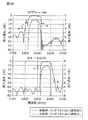
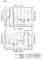
図3Aは、実施例および比較例に係るマルチプレクサのBand25におけるアイソレーション特性を比較したグラフである。 FIG. 3A is a graph comparing the isolation characteristics of the multiplexer according to the example and the comparative example in Band 25.
比較例に係るマルチプレクサでは、Band25の高周波送信信号が、受信フィルタ20が配置されたBand25の受信経路へと漏洩してしまう。
In the multiplexer according to the comparative example, the high frequency transmission signal of the Band 25 leaks to the reception path of the Band 25 in which the
これに対して、実施例に係るマルチプレクサ1Aでは、インダクタ21とインダクタ12とが磁界結合しているため、Band25の送信フィルタ10を通過した高周波送信信号のうち受信フィルタ20に漏洩する高周波成分P25と、送信端子110から磁界結合したインダクタ12および21を経由して受信フィルタ20に向かう高周波成分N25とが位相反転している。これにより、これら2つの高周波成分P25およびN25が打ち消され、特に、Band25の受信帯域(図3Aの破線内領域)においてアイソレーションが改善されていることが解る。
On the other hand, in the
図3Bは、実施例および比較例に係るBand25フィルタの通過特性を比較したグラフである。同図の上段には、Band25の送信フィルタの通過特性の比較が示され、同図の下段には、Band25の受信フィルタの通過特性の比較が示されている。同図の上段に示すように、Band25の受信帯域におけるアイソレーションが改善されたことに伴い、Band25の送信フィルタ10の受信帯域における減衰量も改善されていることが解る。一方、Band25の受信フィルタ20については、インダクタ21および12の磁界結合の有無により、通過特性はほぼ変化しないことが解る。
FIG. 3B is a graph comparing the passing characteristics of the Band 25 filter according to the example and the comparative example. The upper part of the figure shows a comparison of the passing characteristics of the Band 25 transmission filter, and the lower part of the figure shows a comparison of the passing characteristics of the Band 25 receiving filter. As shown in the upper part of the figure, it can be seen that the amount of attenuation in the reception band of the Band 25
図4は、実施例および比較例に係るBand25フィルタの電圧定在波比(VSWR)を表すグラフである。同図の上段には、マルチプレクサをアンテナ端子100側から見た場合のVSWRが示され、同図中段には、マルチプレクサを送信端子110側から見た場合のVSWRが示され、同図下段には、マルチプレクサを受信端子120側から見た場合のVSWRが示されている。
FIG. 4 is a graph showing the voltage standing wave ratio (VSWR) of the Band 25 filter according to Examples and Comparative Examples. The upper part of the figure shows VSWR when the multiplexer is viewed from the
図4に示すように、Band25の送信フィルタおよび受信フィルタについては、インダクタ21および12の磁界結合の有無により、入出力インピーダンスはほぼ変化しないことが解る。
As shown in FIG. 4, it can be seen that the input / output impedance of the Band 25 transmission filter and reception filter does not change depending on the presence or absence of magnetic field coupling between the
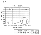
図5Aは、実施例および比較例に係るマルチプレクサのBand66送信フィルタ−Band25受信フィルタのアイソレーション特性を比較したグラフである。 FIG. 5A is a graph comparing the isolation characteristics of the Band 66 transmission filter and the Band 25 reception filter of the multiplexer according to the example and the comparative example.
比較例に係るマルチプレクサでは、Band66の高周波送信信号が、受信フィルタ20が配置されたBand25の受信経路へと漏洩してしまう。
In the multiplexer according to the comparative example, the high frequency transmission signal of the Band 66 leaks to the reception path of the Band 25 in which the
これに対して、実施例に係るマルチプレクサ1Aでは、インダクタ21とインダクタ32とが磁界結合しているため、Band66の送信フィルタ30を通過した高周波送信信号のうち受信フィルタ20に漏洩する高周波成分P66と、送信端子130から磁界結合したインダクタ32および21を経由して受信フィルタ20に向かう高周波成分N66とが位相反転している。これにより、これら2つの高周波成分P66およびN66が打ち消され、特に、Band25の受信帯域(図5Aの破線内領域)においてクロスアイソレーションが改善されていることが解る。
On the other hand, in the
図5Bは、実施例および比較例に係るBand66フィルタの通過特性を比較したグラフである。同図の上段には、Band66の送信フィルタの通過特性の比較が示され、同図の下段には、Band66の受信フィルタの通過特性の比較が示されている。同図の上段に示すように、Band25の受信帯域におけるクロスアイソレーションが改善されたことに伴い、Band66の送信フィルタ30のBand25受信帯域近辺における減衰量も改善されていることが解る。一方、Band66の受信フィルタ40については、インダクタ32および21の磁界結合の有無により、通過特性はほぼ変化しないことが解る。
FIG. 5B is a graph comparing the passing characteristics of the Band 66 filter according to the example and the comparative example. The upper part of the figure shows a comparison of the passing characteristics of the Band 66 transmission filter, and the lower part of the figure shows a comparison of the passing characteristics of the Band 66 receiving filter. As shown in the upper part of the figure, it can be seen that as the cross isolation in the reception band of the Band 25 is improved, the attenuation amount of the
図6は、実施例および比較例に係るBand66フィルタの電圧定在波比(VSWR)を表すグラフである。同図の上段には、マルチプレクサをアンテナ端子100側から見た場合のVSWRが示され、同図中段には、マルチプレクサを送信端子130側から見た場合のVSWRが示され、同図下段には、マルチプレクサを受信端子140側から見た場合のVSWRが示されている。
FIG. 6 is a graph showing the voltage standing wave ratio (VSWR) of the Band 66 filter according to Examples and Comparative Examples. The upper part of the figure shows VSWR when the multiplexer is viewed from the
図6に示すように、Band66の送信フィルタおよび受信フィルタについては、インダクタ32および21の磁界結合の有無により、入出力インピーダンスはほぼ変化しないことが解る。
As shown in FIG. 6, it can be seen that the input / output impedance of the Band 66 transmission filter and reception filter does not change depending on the presence or absence of magnetic field coupling between the
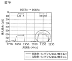
図7Aは、実施例および比較例に係るマルチプレクサのBand66におけるアイソレーション特性を比較したグラフである。実施例および比較例に係るマルチプレクサにおいて、受信フィルタ40が配置された受信経路にはインダクタは配置されていないので、インダクタ32との磁界結合によるアイソレーションの改善効果は見られないと推測される。ただし、インダクタ32および21の磁界結合により、Band66の高周波送信信号のうち受信フィルタ20に漏洩する高周波成分P66が打ち消されているため、Band66の高周波送信信号のうち受信フィルタ40に漏洩する高周波成分も相対的に低減されているものと推測される。これにより、Band66の受信帯域においてもアイソレーションが改善されていることが解る。
FIG. 7A is a graph comparing the isolation characteristics of the multiplexer according to Examples and Comparative Examples in Band 66. In the multiplexer according to the examples and the comparative examples, since the inductor is not arranged in the receiving path in which the receiving
図7Bは、実施例および比較例に係るマルチプレクサのBand25送信フィルタ−Band66受信フィルタのアイソレーション特性を比較したグラフである。実施例および比較例に係るマルチプレクサにおいて、受信フィルタ40が配置された受信経路にはインダクタは配置されていないので、インダクタ12との磁界結合によるクロスアイソレーションの改善効果は見られないと推測される。ただし、インダクタ12および21の磁界結合により、Band25の高周波送信信号のうち受信フィルタ20に漏洩する高周波成分P25が打ち消されているため、Band25の高周波送信信号のうち受信フィルタ40に漏洩する高周波成分も相対的に低減されているものと推測される。これにより、Band66の受信帯域においてもクロスアイソレーションが改善されていることが解る。
FIG. 7B is a graph comparing the isolation characteristics of the Band 25 transmission filter and the Band 66 reception filter of the multiplexer according to Examples and Comparative Examples. In the multiplexers of Examples and Comparative Examples, since the inductor is not arranged in the receiving path where the receiving
(実施の形態2)
本実施の形態では、上記実施例に係るマルチプレクサ1Aを備える高周波フロントエンド回路3および通信装置4について説明する。
(Embodiment 2)
In this embodiment, the high frequency front-
図8は、実施の形態2に係る高周波フロントエンド回路3および通信装置4の回路構成図である。同図には、高周波フロントエンド回路3と、アンテナ素子2と、RF信号処理回路(RFIC)80と、ベースバンド信号処理回路(BBIC)90とが示されている。高周波フロントエンド回路3と、RF信号処理回路80と、ベースバンド信号処理回路90とは、通信装置4を構成している。
FIG. 8 is a circuit configuration diagram of the high frequency
高周波フロントエンド回路3は、実施例に係るマルチプレクサ1Aと、送信側スイッチ61および受信側スイッチ62と、パワーアンプ回路71と、ローノイズアンプ回路72と、を備える。
The high-frequency front-
送信側スイッチ61は、マルチプレクサ1Aの送信端子110および130に個別に接続された2つの選択端子、ならびに、パワーアンプ回路71に接続された共通端子を有するスイッチ回路である。
The
受信側スイッチ62は、マルチプレクサ1Aの受信端子120および140に個別に接続された2つの選択端子、ならびに、ローノイズアンプ回路72に接続された共通端子を有するスイッチ回路である。
The receiving
これら送信側スイッチ61および受信側スイッチ62は、それぞれ、制御部(図示せず)からの制御信号にしたがって、共通端子と所定のバンドに対応する信号経路とを接続する、例えば、SPDT(Single Pole Double Throw)型のスイッチによって構成される。なお、共通端子と接続される選択端子は1つに限らず、複数であってもかまわない。つまり、高周波フロントエンド回路3は、キャリアアグリゲーションに対応してもかまわない。
Each of the transmitting
パワーアンプ回路71は、RF信号処理回路80から出力された高周波信号(ここでは高周波送信信号)を増幅し、送信側スイッチ61およびマルチプレクサ1Aを経由してアンテナ素子2に出力する送信増幅回路である。
The
ローノイズアンプ回路72は、アンテナ素子2、マルチプレクサ1Aおよび受信側スイッチ62を経由した高周波信号(ここでは高周波受信信号)を増幅し、RF信号処理回路80へ出力する受信増幅回路である。
The low-
RF信号処理回路80は、アンテナ素子2から受信信号経路を介して入力された高周波受信信号を、ダウンコンバートなどにより信号処理し、当該信号処理して生成された受信信号をベースバンド信号処理回路90へ出力する。また、RF信号処理回路80は、ベースバンド信号処理回路90から入力された送信信号をアップコンバートなどにより信号処理し、当該信号処理して生成された高周波送信信号をパワーアンプ回路71へ出力する。RF信号処理回路80は、例えば、RFICである。
The RF
ベースバンド信号処理回路90で処理された信号は、例えば、画像信号として画像表示のために、または、音声信号として通話のために使用される。
The signal processed by the baseband
なお、高周波フロントエンド回路3は、上述した各構成要素の間に、他の回路素子を備えていてもよい。
The high-frequency front-
以上のように構成された高周波フロントエンド回路3および通信装置4によれば、上記実施例に係るマルチプレクサ1Aを備えることにより、割り当てられる周波数帯域(バンド)の数が多くなっても、各送信フィルタが配置された送信経路と各受信フィルタが配置された受信経路との間のアイソレーションを向上させることが可能となる。
According to the high-frequency front-
また、通信装置4は、高周波信号の処理方式に応じて、ベースバンド信号処理回路90を備えていなくてもよい。
Further, the communication device 4 does not have to include the baseband
(その他の実施の形態)
以上、本発明の実施の形態に係るマルチプレクサ、高周波フロントエンド回路および通信装置について、実施例および変形例を挙げて説明したが、本発明は、上記実施の形態、実施例および変形例における任意の構成要素を組み合わせて実現される別の実施の形態や、上記実施の形態に対して本発明の主旨を逸脱しない範囲で当業者が思いつく各種変形を施して得られる変形例や、本発明に係る高周波フロントエンド回路および通信装置を内蔵した各種機器も本発明に含まれる。
(Other embodiments)
The multiplexer, high-frequency front-end circuit, and communication device according to the embodiment of the present invention have been described above with reference to examples and modifications. However, the present invention describes any of the above embodiments, examples, and modifications. Another embodiment realized by combining the constituent elements, a modification obtained by performing various modifications that can be conceived by those skilled in the art without departing from the gist of the present invention, and the present invention. Various devices incorporating a high-frequency front-end circuit and a communication device are also included in the present invention.
上記説明では、マルチプレクサとしてBand25+Band66のクワッドプレクサを例に説明したが、本発明は、これに限られず、例えば、3以上のフィルタを有し、それらが共通端子で接続されるマルチプレクサに適用することができる。 In the above description, the quadplexer of Band25 + Band66 has been described as an example as the multiplexer, but the present invention is not limited to this, and is applied to, for example, a multiplexer having three or more filters and connecting them with a common terminal. Can be done.
本発明は、マルチバンド化およびマルチモード化された周波数規格に適用できる高アイソレーションおよび高クロスアイソレーションのマルチプレクサ、高周波フロントエンド回路および通信装置として、携帯電話などの通信機器に広く利用できる。 The present invention can be widely used in communication devices such as mobile phones as high-isolation and high-cross-isolation multiplexers, high-frequency front-end circuits and communication devices applicable to multi-band and multi-mode frequency standards.
1A、1B マルチプレクサ
2 アンテナ素子
3 高周波フロントエンド回路
4 通信装置
10、30 送信フィルタ
12、21、22、31、32、42 インダクタ
20、40 受信フィルタ
50 整合回路
61 送信側スイッチ
62 受信側スイッチ
71 パワーアンプ回路
72 ローノイズアンプ回路
80 RF信号処理回路(RFIC)
90 ベースバンド信号処理回路(BBIC)
100 アンテナ端子
101 共通端子
110、130 送信端子
120、140 受信端子
1A,
90 Baseband Signal Processing Circuit (BBIC)
100 Antenna terminal 101
Claims (9)
前記共通端子と前記第1受信端子との間に配置された第1受信フィルタと、
前記共通端子と前記第1送信端子との間に配置された第1送信フィルタと、
前記共通端子と前記第2送信端子との間に配置された第2送信フィルタと、
前記共通端子と前記第1受信フィルタとの間に直列接続された第1インダクタと、
前記第1送信端子と前記第1送信フィルタとの間に直列接続された第2インダクタと、
前記第2送信端子と前記第2送信フィルタとの間に直列接続された第3インダクタと、を備え、
前記第1インダクタのインダクタンス値は、前記第2インダクタのインダクタンス値よりも大きく、かつ、前記第3インダクタのインダクタンス値よりも大きく、
前記第1送信端子から前記第1送信フィルタを通過した高周波送信信号のうち前記第1受信フィルタに漏洩する高周波成分と、前記第1送信端子から磁界結合した前記第2インダクタおよび前記第1インダクタを経由して前記第1受信フィルタに向かう高周波成分とが位相反転した関係となるように、前記第1インダクタと前記第2インダクタとは磁界結合しており、
前記第2送信端子から前記第2送信フィルタを通過した高周波送信信号のうち前記第1受信フィルタに漏洩する高周波成分と、前記第2送信端子から磁界結合した前記第3インダクタおよび前記第1インダクタを経由して前記第1受信フィルタに向かう高周波成分とが位相反転した関係となるように、前記第1インダクタと前記第3インダクタとは磁界結合している、
マルチプレクサ。 Common terminal, first receiving terminal, first transmitting terminal, and second transmitting terminal,
A first reception filter arranged between the common terminal and the first reception terminal,
A first transmission filter arranged between the common terminal and the first transmission terminal,
A second transmission filter arranged between the common terminal and the second transmission terminal,
A first inductor connected in series between the common terminal and the first receive filter,
A second inductor connected in series between the first transmission terminal and the first transmission filter,
A third inductor connected in series between the second transmission terminal and the second transmission filter is provided.
The inductance value of the first inductor is larger than the inductance value of the second inductor and larger than the inductance value of the third inductor.
Of the high-frequency transmission signals that have passed through the first transmission filter from the first transmission terminal, the high-frequency component that leaks to the first reception filter, and the second inductor and the first inductor that are magnetically coupled from the first transmission terminal. The first inductor and the second inductor are magnetically coupled so that the high-frequency component that goes through the first receiving filter has a phase-inverted relationship .
Of the high-frequency transmission signals that have passed through the second transmission filter from the second transmission terminal, the high-frequency component that leaks to the first reception filter, and the third inductor and the first inductor that are magnetically coupled from the second transmission terminal. The first inductor and the third inductor are magnetically coupled so that the high-frequency component passing through the first receiving filter has a phase-inverted relationship .
Multiplexer.
前記第1送信フィルタは、前記第1送信帯域を通過帯域とし、
前記第2送信フィルタは、前記第1周波数帯域と異なる第2周波数帯域に割り当てられた第2送信帯域および第2受信帯域のうちの前記第2送信帯域を通過帯域とする、
請求項1に記載のマルチプレクサ。 The first reception filter uses the first reception band of the first transmission band and the first reception band assigned to the first frequency band as a pass band.
The first transmission filter uses the first transmission band as a pass band.
The second transmission filter uses the second transmission band of the second transmission band and the second reception band assigned to the second frequency band different from the first frequency band as the pass band.
The multiplexer according to claim 1 .
請求項1または2に記載のマルチプレクサ。 The first receiving filter, the first transmitting filter, and the second transmitting filter may be a surface acoustic wave filter, a surface acoustic wave filter using a BAW (Bulk Acoustic Wave), an LC resonance filter, or a dielectric filter. is there,
The multiplexer according to claim 1 or 2 .
前記共通端子と前記第1送信端子との間に配置された第1送信フィルタと、
前記共通端子と前記第1受信端子との間に配置された第1受信フィルタと、
前記共通端子と前記第2受信端子との間に配置された第2受信フィルタと、
前記共通端子と前記第1送信フィルタとの間に直列接続された第1インダクタと、
前記第1受信端子と前記第1受信フィルタとの間に直列接続された第2インダクタと、
前記第2受信端子と前記第2受信フィルタとの間に直列接続された第3インダクタと、を備え、
前記第1インダクタのインダクタンス値は、前記第2インダクタのインダクタンス値よりも小さく、かつ、前記第3インダクタのインダクタンス値よりも小さく、
前記第1送信端子から前記第1送信フィルタを通過した高周波送信信号のうち前記第1受信フィルタに漏洩する高周波成分と、前記第1送信端子から磁界結合した前記第1インダクタおよび前記第2インダクタを経由して前記第1受信端子に向かう高周波成分とが位相反転した関係となるように、前記第1インダクタと前記第2インダクタとは磁界結合しており、
前記第1送信端子から前記第1送信フィルタを通過した高周波送信信号のうち前記第2受信フィルタに漏洩する高周波成分と、前記第1送信端子から磁界結合した前記第1インダクタおよび前記第3インダクタを経由して前記第2受信端子に向かう高周波成分とが位相反転した関係となるように、前記第1インダクタと前記第3インダクタとは磁界結合している、
マルチプレクサ。 Common terminal, 1st transmission terminal, 1st reception terminal, 2nd reception terminal,
A first transmission filter arranged between the common terminal and the first transmission terminal,
A first reception filter arranged between the common terminal and the first reception terminal,
A second reception filter arranged between the common terminal and the second reception terminal,
A first inductor connected in series between the common terminal and the first transmission filter,
A second inductor connected in series between the first receiving terminal and the first receiving filter,
A third inductor connected in series between the second receiving terminal and the second receiving filter is provided.
The inductance value of the first inductor is smaller than the inductance value of the second inductor and smaller than the inductance value of the third inductor.
The high-frequency component of the high-frequency transmission signal that has passed through the first transmission filter from the first transmission terminal leaks to the first reception filter, and the first inductor and the second inductor that are magnetically coupled from the first transmission terminal. The first inductor and the second inductor are magnetically coupled so that the high-frequency component that goes through the first receiving terminal has a phase-inverted relationship .
The high-frequency component of the high-frequency transmission signal that has passed through the first transmission filter from the first transmission terminal leaks to the second reception filter, and the first inductor and the third inductor that are magnetically coupled from the first transmission terminal. The first inductor and the third inductor are magnetically coupled so that the high-frequency component that goes through the second receiving terminal has a phase-inverted relationship .
Multiplexer.
前記第1受信フィルタは、前記第1受信帯域を通過帯域とし、
前記第2受信フィルタは、前記第1周波数帯域と異なる第2周波数帯域に割り当てられた第2送信帯域および第2受信帯域のうちの前記第2受信帯域を通過帯域とする、
請求項4に記載のマルチプレクサ。 The first transmission filter uses the first transmission band of the first transmission band and the first reception band assigned to the first frequency band as a pass band.
The first reception filter uses the first reception band as a pass band.
The second reception filter uses the second reception band of the second transmission band and the second reception band assigned to the second frequency band different from the first frequency band as the pass band.
The multiplexer according to claim 4 .
請求項4または5に記載のマルチプレクサ。 The first transmission filter, the first reception filter, and the second reception filter are any of a surface acoustic wave filter, a surface acoustic wave filter using a BAW, an LC resonance filter, and a dielectric filter.
The multiplexer according to claim 4 or 5 .
アンテナ素子に接続されるアンテナ端子と、
前記アンテナ端子と前記共通端子との間に接続されたインピーダンス整合回路と、を備える、
請求項1〜6のいずれか1項に記載のマルチプレクサ。 further,
The antenna terminal connected to the antenna element and
An impedance matching circuit connected between the antenna terminal and the common terminal is provided.
The multiplexer according to any one of claims 1 to 6 .
前記マルチプレクサに接続された増幅回路と、を備える、
高周波フロントエンド回路。 The multiplexer according to any one of claims 1 to 7 and
An amplifier circuit connected to the multiplexer.
High frequency front end circuit.
前記アンテナ素子と前記RF信号処理回路との間で前記高周波信号を伝達する請求項8に記載の高周波フロントエンド回路と、を備える、
通信装置。 An RF signal processing circuit that processes high-frequency signals transmitted and received by the antenna element,
The high-frequency front-end circuit according to claim 8 , which transmits the high-frequency signal between the antenna element and the RF signal processing circuit.
Communication device.
Priority Applications (2)
| Application Number | Priority Date | Filing Date | Title |
|---|---|---|---|
| US15/963,569 US10230418B2 (en) | 2017-05-19 | 2018-04-26 | Multiplexer, high-frequency front end circuit, and communication device |
| CN201810445596.4A CN108964633B (en) | 2017-05-19 | 2018-05-10 | Multiplexer, high-frequency front-end circuit and communication device |
Applications Claiming Priority (2)
| Application Number | Priority Date | Filing Date | Title |
|---|---|---|---|
| JP2017099675 | 2017-05-19 | ||
| JP2017099675 | 2017-05-19 |
Publications (2)
| Publication Number | Publication Date |
|---|---|
| JP2018196110A JP2018196110A (en) | 2018-12-06 |
| JP6798521B2 true JP6798521B2 (en) | 2020-12-09 |
Family
ID=64570708
Family Applications (1)
| Application Number | Title | Priority Date | Filing Date |
|---|---|---|---|
| JP2018056147A Active JP6798521B2 (en) | 2017-05-19 | 2018-03-23 | Multiplexers, high frequency front-end circuits and communication equipment |
Country Status (1)
| Country | Link |
|---|---|
| JP (1) | JP6798521B2 (en) |
Families Citing this family (2)
| Publication number | Priority date | Publication date | Assignee | Title |
|---|---|---|---|---|
| JP6919664B2 (en) * | 2019-01-31 | 2021-08-18 | 株式会社村田製作所 | Multiplexer and communication device |
| JP2021048566A (en) * | 2019-09-20 | 2021-03-25 | 株式会社村田製作所 | High frequency module and communication device |
Family Cites Families (5)
| Publication number | Priority date | Publication date | Assignee | Title |
|---|---|---|---|---|
| JP6249020B2 (en) * | 2013-08-06 | 2017-12-20 | 株式会社村田製作所 | High frequency module |
| CN106537793B (en) * | 2014-07-01 | 2019-09-06 | 株式会社村田制作所 | High frequency module |
| CN106464294B (en) * | 2015-02-25 | 2019-03-15 | 株式会社村田制作所 | High frequency module |
| DE112016002335B4 (en) * | 2015-06-24 | 2021-07-01 | Murata Manufacturing Co., Ltd. | Multiplexer, transmitting device, receiving device, high frequency front-end circuit, communication device, and impedance matching method for a multiplexer |
| CN107710628B (en) * | 2015-07-03 | 2020-08-04 | 株式会社村田制作所 | Front end module |
-
2018
- 2018-03-23 JP JP2018056147A patent/JP6798521B2/en active Active
Also Published As
| Publication number | Publication date |
|---|---|
| JP2018196110A (en) | 2018-12-06 |
Similar Documents
| Publication | Publication Date | Title |
|---|---|---|
| US10230418B2 (en) | Multiplexer, high-frequency front end circuit, and communication device | |
| CN108352852B (en) | Switch module | |
| US9917615B2 (en) | Radio-frequency module | |
| US10277191B2 (en) | Composite filter apparatus, high-frequency front end circuit, and communication apparatus | |
| US11545961B2 (en) | Multiplexer and communication apparatus | |
| JP2021064874A (en) | High frequency module and communication device | |
| US11121694B2 (en) | Multiplexer | |
| JP2020205477A (en) | Multiplexer and communication device | |
| US11381261B2 (en) | Radio-frequency module and communication apparatus | |
| US11881844B2 (en) | Multiplexer | |
| JP6798521B2 (en) | Multiplexers, high frequency front-end circuits and communication equipment | |
| CN110247669B (en) | Multiplexer and communication device | |
| JP6822444B2 (en) | Composite filter device, high frequency front end circuit and communication device | |
| US11909382B2 (en) | Multiplexer, front-end module, and communication device | |
| US10425119B2 (en) | High-frequency switch module | |
| US12132508B2 (en) | Radio-frequency circuit and communication device | |
| WO2020184614A1 (en) | Multiplexor, front-end module, and communication device | |
| US12308865B2 (en) | Multiplexer and communication device | |
| CN114731169A (en) | High-frequency circuit, high-frequency front-end circuit, and communication device | |
| US12057878B2 (en) | Radio-frequency circuit and communication device | |
| JP6919664B2 (en) | Multiplexer and communication device | |
| US10951196B2 (en) | Multiplexer, high-frequency front-end circuit, and communication device | |
| JP2021072563A (en) | Multiplexer | |
| WO2024257419A1 (en) | High-frequency circuit and communication device |
Legal Events
| Date | Code | Title | Description |
|---|---|---|---|
| A621 | Written request for application examination |
Free format text: JAPANESE INTERMEDIATE CODE: A621 Effective date: 20191023 |
|
| A977 | Report on retrieval |
Free format text: JAPANESE INTERMEDIATE CODE: A971007 Effective date: 20200730 |
|
| A131 | Notification of reasons for refusal |
Free format text: JAPANESE INTERMEDIATE CODE: A131 Effective date: 20200818 |
|
| A521 | Written amendment |
Free format text: JAPANESE INTERMEDIATE CODE: A523 Effective date: 20201006 |
|
| TRDD | Decision of grant or rejection written | ||
| A01 | Written decision to grant a patent or to grant a registration (utility model) |
Free format text: JAPANESE INTERMEDIATE CODE: A01 Effective date: 20201020 |
|
| A61 | First payment of annual fees (during grant procedure) |
Free format text: JAPANESE INTERMEDIATE CODE: A61 Effective date: 20201102 |
|
| R150 | Certificate of patent or registration of utility model |
Ref document number: 6798521 Country of ref document: JP Free format text: JAPANESE INTERMEDIATE CODE: R150 |