WO2024257419A1 - High-frequency circuit and communication device - Google Patents
High-frequency circuit and communication device Download PDFInfo
- Publication number
- WO2024257419A1 WO2024257419A1 PCT/JP2024/008975 JP2024008975W WO2024257419A1 WO 2024257419 A1 WO2024257419 A1 WO 2024257419A1 JP 2024008975 W JP2024008975 W JP 2024008975W WO 2024257419 A1 WO2024257419 A1 WO 2024257419A1
- Authority
- WO
- WIPO (PCT)
- Prior art keywords
- band
- frequency
- terminal
- signal
- filter
- Prior art date
- Legal status (The legal status is an assumption and is not a legal conclusion. Google has not performed a legal analysis and makes no representation as to the accuracy of the status listed.)
- Ceased
Links
Images








Classifications
-
- H—ELECTRICITY
- H04—ELECTRIC COMMUNICATION TECHNIQUE
- H04B—TRANSMISSION
- H04B1/00—Details of transmission systems, not covered by a single one of groups H04B3/00 - H04B13/00; Details of transmission systems not characterised by the medium used for transmission
- H04B1/06—Receivers
- H04B1/10—Means associated with receiver for limiting or suppressing noise or interference
-
- H—ELECTRICITY
- H04—ELECTRIC COMMUNICATION TECHNIQUE
- H04B—TRANSMISSION
- H04B1/00—Details of transmission systems, not covered by a single one of groups H04B3/00 - H04B13/00; Details of transmission systems not characterised by the medium used for transmission
-
- H—ELECTRICITY
- H04—ELECTRIC COMMUNICATION TECHNIQUE
- H04B—TRANSMISSION
- H04B1/00—Details of transmission systems, not covered by a single one of groups H04B3/00 - H04B13/00; Details of transmission systems not characterised by the medium used for transmission
- H04B1/005—Details of transmission systems, not covered by a single one of groups H04B3/00 - H04B13/00; Details of transmission systems not characterised by the medium used for transmission adapting radio receivers, transmitters andtransceivers for operation on two or more bands, i.e. frequency ranges
- H04B1/0053—Details of transmission systems, not covered by a single one of groups H04B3/00 - H04B13/00; Details of transmission systems not characterised by the medium used for transmission adapting radio receivers, transmitters andtransceivers for operation on two or more bands, i.e. frequency ranges with common antenna for more than one band
- H04B1/0057—Details of transmission systems, not covered by a single one of groups H04B3/00 - H04B13/00; Details of transmission systems not characterised by the medium used for transmission adapting radio receivers, transmitters andtransceivers for operation on two or more bands, i.e. frequency ranges with common antenna for more than one band using diplexing or multiplexing filters for selecting the desired band
-
- H—ELECTRICITY
- H04—ELECTRIC COMMUNICATION TECHNIQUE
- H04B—TRANSMISSION
- H04B1/00—Details of transmission systems, not covered by a single one of groups H04B3/00 - H04B13/00; Details of transmission systems not characterised by the medium used for transmission
- H04B1/005—Details of transmission systems, not covered by a single one of groups H04B3/00 - H04B13/00; Details of transmission systems not characterised by the medium used for transmission adapting radio receivers, transmitters andtransceivers for operation on two or more bands, i.e. frequency ranges
- H04B1/0053—Details of transmission systems, not covered by a single one of groups H04B3/00 - H04B13/00; Details of transmission systems not characterised by the medium used for transmission adapting radio receivers, transmitters andtransceivers for operation on two or more bands, i.e. frequency ranges with common antenna for more than one band
- H04B1/006—Details of transmission systems, not covered by a single one of groups H04B3/00 - H04B13/00; Details of transmission systems not characterised by the medium used for transmission adapting radio receivers, transmitters andtransceivers for operation on two or more bands, i.e. frequency ranges with common antenna for more than one band using switches for selecting the desired band
-
- H—ELECTRICITY
- H04—ELECTRIC COMMUNICATION TECHNIQUE
- H04B—TRANSMISSION
- H04B1/00—Details of transmission systems, not covered by a single one of groups H04B3/00 - H04B13/00; Details of transmission systems not characterised by the medium used for transmission
- H04B1/38—Transceivers, i.e. devices in which transmitter and receiver form a structural unit and in which at least one part is used for functions of transmitting and receiving
- H04B1/40—Circuits
- H04B1/50—Circuits using different frequencies for the two directions of communication
Definitions
- the present invention relates to high-frequency circuits and communication devices.
- Multiband front-end circuits are required to transmit and receive multiple high-frequency signals with low loss and high isolation.
- Patent Document 1 discloses a high-frequency module (high-frequency circuit) in which multiple filters with different passbands are connected to an antenna via a multiplexer (switch).
- 3GPP (3rd Generation Partnership Project) is considering simultaneous transmission of signals in two communication bands with partially overlapping frequency bands.
- the present invention aims to provide a small high-frequency circuit and communication device that can simultaneously transmit signals in two communication bands with partially overlapping frequency bands while minimizing degradation of isolation and reception sensitivity.
- a high-frequency circuit comprises a first filter having a passband including a first frequency band, which is one of the transmission band and reception band of a first communication band, and a second filter having a passband including a second frequency band, which is the other of the transmission band and reception band of a second communication band, the first communication band and the second communication band being a band combination capable of simultaneous communication, the first frequency band including a first subband that overlaps with the second frequency band and a second subband that does not overlap with the second frequency band, the second frequency band including the first subband and a third subband that does not overlap with the first communication band, and the passband of the first filter is variable to a first passband including the first subband and the second subband, and a second passband including the second subband and narrower than the first passband.
- the present invention makes it possible to provide a small high-frequency circuit and communication device that can simultaneously transmit signals in two communication bands with partially overlapping frequency bands while minimizing degradation of isolation and reception sensitivity.
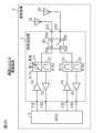
- FIG. 1 is a circuit configuration diagram of a high-frequency circuit and a communication device according to an embodiment.
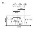
- FIG. 2 is a diagram illustrating the frequency relationship of communication bands and the pass characteristics of filters applied to the high-frequency circuit according to the embodiment.
- FIG. 3A is a circuit diagram showing a connection state of a first switch when a signal in a first communication band is transmitted alone in the high-frequency circuit according to the embodiment.
- FIG. 3B is a circuit diagram showing a connection state of the first switch when signals in the first communication band and signals in the second communication band are transmitted simultaneously in the high-frequency circuit according to the embodiment.
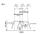
- FIG. 4A is a diagram illustrating the frequency relationship of communication bands and the pass characteristics of filters applied to the high-frequency circuit according to the first modification.
- FIG. 4B is a diagram illustrating the frequency relationship of communication bands and the pass characteristics of filters applied to the high-frequency circuit according to the second modification.
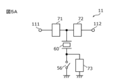
- FIG. 5A is a diagram illustrating a first example of a circuit configuration of a first filter according to an embodiment.
- FIG. 5B is a diagram illustrating a second example of the circuit configuration of the first filter according to the embodiment.
- FIG. 5C is a diagram illustrating a third example of a circuit configuration of the first filter according to the embodiment.
- FIG. 6 is a diagram illustrating the frequency relationship of communication bands and the pass characteristics of filters applied to the high-frequency circuit according to the third modification.
- FIG. 7A is a circuit configuration diagram showing a first connection state of a high-frequency circuit according to Modification 4. As shown in FIG. FIG.
- FIG. 7B is a diagram illustrating the frequency relationship of communication bands applied to the high-frequency circuit according to the fourth modification, and the pass characteristic of a filter in the first connection state.
- FIG. 8A is a circuit configuration diagram showing a second connection state of the high-frequency circuit according to the fourth modification.
- FIG. 8B is a diagram illustrating the frequency relationship of communication bands applied to the high-frequency circuit according to the fourth modification, and the pass characteristic of the filter in the second connection state.
- FIG. 9A is a circuit configuration diagram of a high-frequency circuit and a diverter circuit according to a fifth modified example.
- FIG. 9B is a circuit configuration diagram of a high-frequency circuit and a primary circuit according to Modification 6.
- each figure is a schematic diagram in which emphasis, omissions, or adjustments to the ratio have been made as appropriate to illustrate the present invention, and is not necessarily an exact illustration, and may differ from the actual shape, positional relationship, and ratio.
- the same reference numerals are used for substantially the same configuration, and duplicate explanations may be omitted or simplified.
- connection refers not only to direct connection by a connection terminal and/or wiring conductor, but also to electrical connection via other circuit elements. Additionally, “connected between A and B” refers to connection to A and B on the path connecting A and B.
- a "transmission path” refers to a transmission line that is composed of a wiring through which a high-frequency transmission signal propagates, an electrode directly connected to the wiring, and a terminal directly connected to the wiring or the electrode.
- a “reception path” refers to a transmission line that is composed of a wiring through which a high-frequency reception signal propagates, an electrode directly connected to the wiring, and a terminal directly connected to the wiring or the electrode.
- the passband of a filter is defined as the frequency band between two frequencies that are 3 dB greater than the minimum insertion loss within the passband.
- Fig. 1 is a circuit configuration diagram of a high-frequency circuit 1 and a communication device 4 according to the embodiment.
- the communication device 4 includes a high-frequency circuit 1, antennas 2a and 2b, and an RF signal processing circuit (RFIC) 3.
- RFIC RF signal processing circuit
- the high-frequency circuit 1 transmits high-frequency signals between the antennas 2a and 2b and the RFIC 3.
- the detailed circuit configuration of the high-frequency circuit 1 will be described later.
- Antenna 2a is connected to antenna terminal 101 of high frequency circuit 1, and transmits high frequency signals output from high frequency circuit 1, and also receives high frequency signals from the outside and outputs them to high frequency circuit 1.
- Antenna 2b is connected to antenna terminal 102 of high frequency circuit 1, and transmits high frequency signals output from high frequency circuit 1, and also receives high frequency signals from the outside and outputs them to high frequency circuit 1.
- the RFIC3 is an example of a signal processing circuit that processes high-frequency signals. Specifically, the RFIC3 processes the high-frequency received signal input via the receiving path of the high-frequency circuit 1 by down-conversion or the like, and outputs the received signal generated by the signal processing to a baseband signal processing circuit (BBIC: not shown). The RFIC3 also processes the transmission signal input from the BBIC by up-conversion or the like, and outputs the high-frequency transmission signal generated by the signal processing to the transmitting path of the high-frequency circuit 1. The RFIC3 also has a control unit that controls the switches and amplifiers of the high-frequency circuit 1. Note that some or all of the functions of the RFIC3 as a control unit may be implemented outside the RFIC3, for example, in the BBIC or the high-frequency circuit 1.
- antennas 2a and 2b are not essential components of communication device 4 in this embodiment.
- the high-frequency circuit 1 includes filters 11, 12, 21, and 22, a switch 50, power amplifiers 31 and 41, low-noise amplifiers 32 and 42, antenna terminals 101 and 102, high-frequency input terminals 110 and 130, and high-frequency output terminals 120 and 140.
- the antenna terminal 101 is connected to the antenna 2a and the terminal 50a of the switch 50.
- the antenna terminal 102 is connected to the antenna 2b and the terminal 50b of the switch 50.
- the radio frequency input terminal 110 is connected to the RFIC 3 and the power amplifier 31, and is a terminal for receiving a radio frequency transmission signal from the RFIC 3.
- the radio frequency input terminal 130 is connected to the RFIC 3 and the power amplifier 41, and is a terminal for receiving a radio frequency transmission signal from the RFIC 3.
- the radio frequency output terminal 120 is connected to the RFIC 3 and the low noise amplifier 32, and is a terminal for outputting a radio frequency reception signal to the RFIC 3.
- the radio frequency output terminal 140 is connected to the RFIC 3 and the low noise amplifier 42, and is a terminal for outputting a radio frequency reception signal to the RFIC 3.
- FIG. 2 illustrates the frequency relationship between communication band A and communication band B applied to high-frequency circuit 1 according to the embodiment, and the pass characteristics of filters 11 and 22.
- communication band A is an example of a first communication band
- communication band B is an example of a second communication band.
- Communication band A and communication band B are a band combination that allows simultaneous communication. As shown in FIG. 2, the transmission band (A-Tx) of communication band A and the reception band (B-Rx) of communication band B partially overlap in frequency.
- the transmission band of communication band A is an example of a first frequency band
- the reception band of communication band B is an example of a second frequency band.
- the transmission band of communication band A includes subband X (first subband) that overlaps with the reception band of communication band B, and subband Y (second subband) that does not overlap with the reception band of communication band B.
- the reception band of communication band B includes subband X (first subband) that overlaps with the transmission band of communication band A, and subband Z (third subband) that does not overlap with the transmission band of communication band A.
- one band partially overlaps with another band does not only mean that a portion of the frequency range of one band overlaps with a portion of the frequency range of the other band, but also means that a point at the low frequency end or high frequency end of one band coincides with a point at the high frequency end or low frequency end of the other band, but does not coincide at other frequencies.
- subband X may be composed of only one predetermined frequency point.
- each of communication band A, communication band B, and communication band C and communication band D described below means a frequency band predefined by a standardization organization (e.g., 3GPP (registered trademark), IEEE (Institute of Electrical and Electronics Engineers), etc.) for a communication system constructed using radio access technology (RAT).
- a standardization organization e.g., 3GPP (registered trademark), IEEE (Institute of Electrical and Electronics Engineers), etc.
- RAT radio access technology
- Examples of communication systems that can be used include, but are not limited to, an LTE (Long Term Evolution) system, a 5G (5th Generation)-NR (New Radio) system, and a WLAN (Wireless Local Area Network) system.
- Filter 11 is an example of a first filter, and has a passband that includes the transmission band (first frequency band) of communication band A. More specifically, the passband of filter 11 is variable between a first passband that includes subband X and subband Y, and a second passband that includes subband Y and is narrower than the first passband. In other words, filter 11 varies between a first characteristic having a first passband and a second characteristic having a second passband, for example, by a control signal output from RFIC 3. One end of filter 11 is connected to terminal 50c (first terminal) of switch 50 (first switch), and the other end of filter 11 is connected to the output terminal of power amplifier 31.
- Filter 22 is an example of a second filter, and has a pass band that includes the reception band (second frequency band) of communication band B.
- One end of filter 22 is connected to terminal 50d (second terminal) of switch 50 (first switch), and the other end of filter 22 is connected to the input terminal of low-noise amplifier 42.
- the filter 12 has a pass band that includes the reception band of the communication band A.
- One end of the filter 12 is connected to the terminal 50c of the switch 50, and the other end of the filter 12 is connected to the input terminal of the low noise amplifier 32.
- the filter 21 has a passband that includes the transmission band of the communication band B. One end of the filter 21 is connected to the terminal 50d of the switch 50, and the other end of the filter 21 is connected to the output terminal of the power amplifier 41.
- Switch 50 is an example of a first switch, and has terminal 50a (first antenna connection terminal), terminal 50b (second antenna connection terminal), terminal 50c (first terminal), and terminal 50d (second terminal).
- Switch 50 is a DPDT (Double Pole Double Throw) type switch, and switches between connection and non-connection between terminals 50a and 50c, between connection and non-connection between terminals 50a and 50d, between connection and non-connection between terminals 50b and 50c, and between connection and non-connection between terminals 50b and 50d.
- Terminal 50a is connected to antenna terminal 101
- terminal 50b is connected to antenna terminal 102
- terminal 50c is connected to filters 11 and 12
- terminal 50d is connected to filters 21 and 22.
- the switch 50 switches between the connection and disconnection between the antenna 2a and the filters 11 and 12, between the connection and disconnection between the antenna 2a and the filters 21 and 22, between the connection and disconnection between the antenna 2b and the filters 11 and 12, and between the connection and disconnection between the antenna 2b and the filters 21 and 22.
- the power amplifier 31 has an output terminal connected to the filter 11 and an input terminal connected to the radio frequency input terminal 110.
- the power amplifier 31 amplifies the radio frequency transmission signal (hereinafter referred to as the transmission signal) of the communication band A input from the radio frequency input terminal 110.
- the output terminal of the power amplifier 41 is connected to the filter 21, and the input terminal is connected to the radio frequency input terminal 130.
- the power amplifier 41 amplifies the transmission signal of the communication band B input from the radio frequency input terminal 130.
- the input terminal of the low-noise amplifier 32 is connected to the filter 12, and the output terminal is connected to the high-frequency output terminal 120.
- the low-noise amplifier 32 amplifies the high-frequency reception signal (hereinafter referred to as the reception signal) of the communication band A input from the antenna terminal 101 or 102.
- the input terminal of the low noise amplifier 42 is connected to the filter 22, and the output terminal is connected to the high frequency output terminal 140.
- the low noise amplifier 42 amplifies the received signal of the communication band B input from the antenna terminal 101 or 102.
- the high frequency circuit 1 can execute (1) a first mode in which a transmission signal of sub-band Y of communication band A and a reception signal of sub-band Z of communication band B are simultaneously transmitted, (2) a second mode in which a transmission signal of communication band A is transmitted but a reception signal of communication band B is not transmitted, and (3) a third mode in which a reception signal of communication band B is transmitted but a transmission signal of communication band A is not transmitted.
- FIG. 3A is a circuit diagram showing the connection state of the switch 50 when a signal of communication band A is transmitted alone in the high-frequency circuit 1 according to the embodiment.
- FIG. 3B is a circuit diagram showing the connection state of the switch 50 when a transmission signal of communication band A and a reception signal of communication band B are simultaneously transmitted in the high-frequency circuit 1 according to the embodiment.
- the filter 11 when the second mode is executed, the filter 11 is set to the first passband, so that the transmission signal of the communication band A can be transmitted using the entire transmission band of the communication band A.
- the terminals 50a and 50c of the switch 50 are connected as shown in FIG. 3A. Furthermore, when the second mode is executed, it is desirable to disconnect the terminals 50b and 50d of the switch 50. This allows the transmission signal of the communication band A that passes through the filter 11 to be transmitted with low loss.
- the received signal of communication band B can be transmitted using filter 22. Furthermore, when the third mode is executed, terminals 50b and 50d of switch 50 are connected. Furthermore, when the third mode is executed, it is desirable to disconnect terminals 50a and 50c of switch 50. This allows the received signal of communication band B that passes through filter 22 to be transmitted with low loss.
- the filter 11 When the first mode is executed, the filter 11 is set to the second passband, and as shown in FIG. 3B, the terminals 50a and 50c of the switch 50 are connected, and the terminals 50b and 50d are connected. This improves the isolation between the transmission signal of communication band A that passes through the filter 11 and the reception signal of communication band B that passes through the filter 22, and suppresses deterioration of the reception sensitivity of communication band B.
- a so-called coband filter is used that has a passband that includes the partially overlapping transmission band of communication band A and the reception band of communication band B.
- the transmission signal of communication band A it is not possible to prevent the transmission signal of communication band A from leaking into the reception path of communication band B via the coband filter, resulting in a deterioration in the reception sensitivity of communication band B.
- a second example of a conventional configuration for implementing the first mode is one that includes a first high-frequency circuit for transmitting a transmission signal in communication band A and a second high-frequency circuit for transmitting a reception signal in communication band B, with the first and second high-frequency circuits being completely separated.
- the first and second high-frequency circuits are close to each other, the mutual interference between the transmission signal in communication band A and the reception signal in communication band B will become stronger, resulting in poor isolation.
- the circuit will become larger.
- the passband of the filter 11 is variable, so that even if the filter 11 and the filter 22 are placed close to each other, mutual interference between the transmission signal of the communication band A and the reception signal of the communication band B during execution of the first mode can be suppressed, and isolation can be ensured. Therefore, it is possible to provide a small-sized high-frequency circuit 1 that can simultaneously transmit the transmission signal of the communication band A and the reception signal of the communication band B while suppressing the deterioration of isolation and reception sensitivity.
- the switch 50 may be an SPDT (Single Pole Double Throw) type switch instead of a DPDT type switch.
- the first switch has one antenna connection terminal, a first terminal, and a second terminal, and switches between connection and non-connection between the antenna connection terminal and the first terminal, and between connection and non-connection between the antenna connection terminal and the second terminal.
- the antenna connection terminal is connected to one antenna, the first terminal is connected to filters 11 and 12, and the second terminal is connected to filters 21 and 22.
- the filter 11 when the second mode is executed, the filter 11 is set to the first passband, so that the transmission signal of the communication band A can be transmitted using the entire transmission band of the communication band A. Furthermore, when the second mode is executed, the antenna connection terminal of the first switch is connected to the first terminal. Furthermore, when the second mode is executed, it is desirable to disconnect the antenna connection terminal of the first switch from the second terminal. This allows the transmission signal of the communication band A that passes through the filter 11 to be transmitted with low loss.
- the first switch is an SPDT type switch
- the third mode when the third mode is executed, the received signal of communication band B can be transmitted using filter 22.
- the antenna connection terminal and the second terminal of the first switch are connected.
- the filter 11 when the first mode is executed, the filter 11 is set to the second passband, the antenna connection terminal of the first switch is connected to the first terminal, and the antenna connection terminal is connected to the second terminal.
- This improves the isolation between the transmission signal of communication band A passing through the filter 11 and the reception signal of communication band B passing through the filter 22, and suppresses deterioration of the reception sensitivity of communication band B.
- the filters 11 and 22 are essential components, and other circuit elements are not necessary.
- the communication band A is, for example, either band 8 for 4G-LTE (transmission band: 880-915MHz, reception band: 925-960MHz) or band n8 for 5G-NR (transmission band: 880-915MHz, reception band: 925-960MHz), and the communication band B is, for example, either band 5 for 4G-LTE (transmission band: 824-849MHz, reception band: 869-894MHz) or band n5 for 5G-NR (transmission band: 824-849MHz, reception band: 869-894MHz).
- the filter 11 may not vary the pass band, and the filter 22 may vary the pass band.
- the high frequency circuit according to the first modification includes filters 11, 12, 21 and 22, a switch 50, power amplifiers 31 and 41, low noise amplifiers 32 and 42, antenna terminals 101 and 102, high frequency input terminals 110 and 130, and high frequency output terminals 120 and 140.
- the high frequency circuit according to this modification differs from the high frequency circuit 1 according to the embodiment only in that filter 11 is a filter with a fixed pass band and filter 22 is a filter with a variable pass band.
- filter 11 is a filter with a fixed pass band
- filter 22 is a filter with a variable pass band.
- FIG. 4A is a diagram illustrating the frequency relationship between communication band A and communication band B applied to a high-frequency circuit according to the first variation of the embodiment, and the pass characteristics of filters 11 and 22.
- communication band A is an example of a second communication band
- communication band B is an example of a first communication band.
- Communication band A and communication band B are a band combination that allows simultaneous communication. As shown in FIG. 4A, the transmission band (A-Tx) of communication band A and the reception band (B-Rx) of communication band B partially overlap in frequency.
- the reception band of communication band B is an example of a first frequency band
- the transmission band of communication band A is an example of a second frequency band.
- the reception band of communication band B includes subband X (first subband) that overlaps with the transmission band of communication band A, and subband Z (second subband) that does not overlap with the transmission band of communication band A.
- the transmission band of communication band A includes subband X (first subband) that overlaps with the reception band of communication band B, and subband Y (third subband) that does not overlap with the reception band of communication band B.
- Filter 22 is an example of a first filter, and has a passband that includes the reception band (first frequency band) of communication band B. More specifically, filter 22 varies a first passband that includes subband X and subband Z, and a second passband that includes subband Z and is narrower than the first passband. In other words, filter 22 varies a third characteristic having the first passband, and a fourth characteristic having the second passband. One end of filter 22 is connected to terminal 50d (first terminal) of switch 50 (first switch), and the other end of filter 22 is connected to the input end of low-noise amplifier 42.
- Filter 11 is an example of a second filter, and has a passband that includes the transmission band (second frequency band) of communication band A. One end of filter 11 is connected to terminal 50c (second terminal) of switch 50 (first switch), and the other end of filter 11 is connected to the input terminal of power amplifier 31.
- Switch 50 is an example of a first switch and has terminal 50a (first antenna connection terminal), terminal 50b (second antenna connection terminal), terminal 50c (second terminal), and terminal 50d (first terminal).
- the high-frequency circuit according to this modified example can execute (1) a first mode in which a transmit signal in subband Y of communication band A and a receive signal in subband Z of communication band B are simultaneously transmitted, (2) a second mode in which a transmit signal in communication band A is transmitted but a receive signal in communication band B is not transmitted, and (3) a third mode in which a receive signal in communication band B is transmitted but a transmit signal in communication band A is not transmitted.
- the filter 22 when the third mode is executed, the filter 22 is set to the first passband, so that the reception signal of the communication band B can be transmitted using the entire reception band of the communication band B. Also, when the second mode is executed, the transmission signal of the communication band A can be transmitted using the filter 11. Also, when the first mode is executed, the filter 22 is set to the second passband, so that the isolation between the reception signal of the communication band B that passes through the filter 22 and the transmission signal of the communication band A that passes through the filter 11 can be improved, and the deterioration of the reception sensitivity of the communication band B can be suppressed.
- the passband of filter 22 is variable, so that even if filter 11 and filter 22 are placed close to each other, mutual interference between the transmission signal of communication band A and the reception signal of communication band B during execution of the first mode can be suppressed, and isolation can be ensured. Therefore, a small-sized high-frequency circuit can be provided that can simultaneously transmit the transmission signal of communication band A and the reception signal of communication band B while suppressing the deterioration of isolation and reception sensitivity.
- communication band A is, for example, either band 8 for 4G-LTE or band n8 for 5G-NR
- communication band B is, for example, either band 5 for 4G-LTE or band n5 for 5G-NR.
- both the filters 11 and 22 may have variable passbands.
- the high-frequency circuit according to the second modification includes filters 11, 12, 21, and 22, a switch 50, power amplifiers 31 and 41, low-noise amplifiers 32 and 42, antenna terminals 101 and 102, high-frequency input terminals 110 and 130, and high-frequency output terminals 120 and 140.
- the high-frequency circuit according to this modification differs from the high-frequency circuit 1 according to the embodiment only in that both filters 11 and 22 are filters with variable passbands.
- FIG. 4B is a diagram illustrating the frequency relationship between communication band A and communication band B applied to the high-frequency circuit according to the second modification of the embodiment, and the pass characteristics of filters 11 and 22.
- communication band A is an example of a first communication band
- communication band B is an example of a second communication band.
- Communication band A and communication band B are a band combination that allows simultaneous communication.
- the transmission band (A-Tx) of communication band A and the reception band (B-Rx) of communication band B partially overlap in frequency.
- the transmission band of communication band A is an example of a first frequency band
- the reception band of communication band B is an example of a second frequency band.
- the transmission band of communication band A includes subband X (first subband) that overlaps with the reception band of communication band B, and subband Y (second subband) that does not overlap with the reception band of communication band B.
- the reception band of communication band B includes subband X (first subband) that overlaps with the transmission band of communication band A, and subband Z (third subband) that does not overlap with the transmission band of communication band A.
- Filter 11 is an example of a first filter, and has a passband that includes the transmission band (first frequency band) of communication band A. More specifically, filter 11 varies a first passband that includes subband X and subband Y, and a second passband that includes subband Y and is narrower than the first passband. In other words, filter 11 varies a first characteristic having a first passband, and a second characteristic having a second passband. One end of filter 11 is connected to terminal 50c (first terminal) of switch 50 (first switch), and the other end of filter 11 is connected to the output terminal of power amplifier 31.
- Filter 22 is an example of a second filter, and has a passband that includes the reception band (second frequency band) of communication band B. More specifically, filter 22 varies a third passband that includes subband X and subband Z, and a fourth passband that includes subband Z and is narrower than the third passband. In other words, filter 22 varies a third characteristic having a third passband, and a fourth characteristic having a fourth passband.
- One end of filter 22 is connected to terminal 50d (second terminal) of switch 50 (first switch), and the other end of filter 22 is connected to the input end of low-noise amplifier 42.
- the high-frequency circuit according to this modified example can execute (1) a first mode in which a transmit signal in subband Y of communication band A and a receive signal in subband Z of communication band B are simultaneously transmitted, (2) a second mode in which a transmit signal in communication band A is transmitted but a receive signal in communication band B is not transmitted, and (3) a third mode in which a receive signal in communication band B is transmitted but a transmit signal in communication band A is not transmitted.
- the filter 11 when the second mode is executed, the filter 11 is set to the first passband, so that the transmission signal of the communication band A can be transmitted using the entire transmission band of the communication band A. Furthermore, when the third mode is executed, the filter 22 can be used to transmit the reception signal of the communication band B. Furthermore, when the first mode is executed, the filter 11 is set to the second passband, and the filter 22 is set to the fourth passband, so that the mutual interference between the transmission signal of the communication band A passing through the filter 11 and the reception signal of the communication band B passing through the filter 22 can be further suppressed, improving isolation and suppressing deterioration of the reception sensitivity of the reception signal of the communication band B.
- the passbands of filters 11 and 22 are variable, so that high isolation between the transmission signal of communication band A and the reception signal of communication band B during execution of the first mode can be ensured even if filters 11 and 22 are placed close to each other. Therefore, it is possible to provide a small-sized high-frequency circuit that can simultaneously transmit the transmission signal of communication band A and the reception signal of communication band B while suppressing deterioration of isolation and reception sensitivity.
- communication band A is, for example, either band 8 for 4G-LTE or band n8 for 5G-NR
- communication band B is, for example, either band 5 for 4G-LTE or band n5 for 5G-NR.
- FIG. 5A is a diagram showing a first example of the circuit configuration of a filter 11 according to an embodiment.
- FIG. 5B is a diagram showing a second example of the circuit configuration of a filter 11 according to an embodiment.
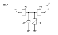
- FIG. 5C is a diagram showing a third example of the circuit configuration of a filter 11 according to an embodiment.
- the filter 11 shown in FIG. 5A includes circuit elements 71, 72, and 73, a switch 56, and an elastic wave resonator 60.
- the circuit elements 71 and 72 are connected in series on a series arm path connecting the terminals 111 and 112.
- the elastic wave resonator 60 is connected between the connection point of the circuit elements 71 and 72 and ground.
- the switch 56 is connected in series with the elastic wave resonator 60 on a parallel arm path connecting the connection point and ground.
- the circuit element 73 is connected in parallel to the switch 56.
- Each of the circuit elements 71, 72, and 73 is, for example, any one of an inductor, a capacitor, and an elastic wave resonator.
- the resonance bandwidth (frequency difference between the antiresonance frequency and the resonance frequency) of the elastic wave resonator 60 is variable depending on whether the switch 51 is conductive or non-conductive.
- the pass band of the filter 11 in this example is variable depending on whether the switch 56 is conductive or non-conductive.
- the filter 11 shown in FIG. 5B includes circuit elements 71, 72, and 73, a switch 56, and an elastic wave resonator 60.
- the circuit elements 71 and 72 are connected in series on a series arm path connecting terminals 111 and 112.
- the elastic wave resonator 60 is connected between the connection point of the circuit elements 71 and 72 and ground.
- the series connection circuit of the switch 56 and the circuit element 73 is connected in parallel to the elastic wave resonator 60.
- Each of the circuit elements 71, 72, and 73 is, for example, any one of an inductor, a capacitor, and an elastic wave resonator.
- the resonance bandwidth of the elastic wave resonator 60 is variable depending on whether the switch 56 is conductive or non-conductive.
- the passband of the filter 11 in this example is variable depending on whether the switch 56 is conductive or non-conductive.
- the filter 11 shown in FIG. 5C includes circuit elements 71 and 72, a variable circuit element 74, and an elastic wave resonator 60.
- the circuit elements 71 and 72 are connected in series on a series arm path connecting the terminals 111 and 112.
- the elastic wave resonator 60 is connected between the connection point of the circuit elements 71 and 72 and ground.
- the variable circuit element 74 is connected between the connection point of the circuit elements 71 and 72 and ground.
- Each of the circuit elements 71 and 72 is, for example, any of an inductor, a capacitor, and an elastic wave resonator.
- the variable circuit element 74 is, for example, any of a variable inductor and a variable capacitor.
- the variable circuit element 74 may be composed of an inductor, a capacitor, an elastic wave resonator, and a switch.
- the resonance bandwidth of the elastic wave resonator 60 is variable by varying the physical quantity (inductance value or capacitance value) of the variable circuit element 74.
- the pass band of the filter 11 in this example is variable by varying the physical quantity of the variable circuit element 74.
- the passband of the filter 11 may include one of the transmission band and the reception band of the communication band C (third communication band).
- the high frequency circuit according to the third modification includes filters 11, 12, 21 and 22, a switch 50, power amplifiers 31 and 41, low noise amplifiers 32 and 42, antenna terminals 101 and 102, high frequency input terminals 110 and 130, and high frequency output terminals 120 and 140.
- the high frequency circuit according to this modification differs from the high frequency circuit 1 according to the embodiment only in that the pass band of filter 11 includes the transmission band of communication band C (third communication band).
- the description of the high frequency circuit according to this modification that is the same as that of the high frequency circuit 1 according to the embodiment will be omitted, and the description will focus on the different configurations.
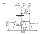
- FIG. 6 is a diagram illustrating the frequency relationship of communication bands A, B, and C applied to a high-frequency circuit according to the third modified embodiment, and the pass characteristics of filters 11 and 22.
- communication band A is an example of a first communication band
- communication band B is an example of a second communication band.
- Communication bands A and B are a band combination that allows simultaneous communication.
- the transmission band (A-Tx) of communication band A and the reception band (B-Rx) of communication band B partially overlap in frequency.
- the transmission band (C-Tx) of communication band C overlaps with sub-band Y of the transmission band of communication band A, but does not overlap with sub-band X.
- Filter 11 is an example of a first filter, and has a passband that includes the transmission band of communication band A (first frequency band) and the transmission band of communication band C.
- the high-frequency circuit according to variant 3 can execute (1) a first mode in which a transmission signal of subband Y of communication band A and a reception signal of subband Z of communication band B are simultaneously transmitted; (2) a second mode in which a transmission signal of communication band A is transmitted but a reception signal of communication band B is not transmitted; (3) a third mode in which a reception signal of communication band B is transmitted but a transmission signal of communication band A is not transmitted; and (4) a fourth mode in which a transmission signal of communication band C is transmitted.
- the signal quality of the transmission signal of communication band C that passes through filter 11 can be improved by setting filter 11 to the second passband.
- the transmission band of the communication band C may overlap with the sub-band X.
- the transmission signal of the communication band C can be transmitted using the entire transmission band of the communication band C by setting the filter 11 to the first passband.
- the transmission band of communication band A it is possible for the transmission band of communication band A to overlap with the reception band of communication band C, rather than the transmission band of communication band C.
- the filter 11 when transmitting a reception signal of communication band C, the filter 11 can be set to the second passband to suppress deterioration of the reception sensitivity of communication band C.
- the passband of the filter 22 may include one of the transmission band and reception band of the communication band C (third communication band).
- the quality of the transmission signal of the communication band C can be improved or the deterioration of the reception sensitivity of the communication band C can be suppressed by setting the filter 22 to the third passband or the fourth passband.
- the passband of filter 11 or the passband of filter 22 may include one of the transmission band and reception band of communication band C (third communication band).
- the passband of filter 11 or the passband of filter 22 may include one of the transmission band and reception band of communication band C (third communication band).
- the quality of the transmission signal of communication band C can be improved, or the deterioration of the reception sensitivity of communication band C can be suppressed.
- communication band A is, for example, either band 8 for 4G-LTE or band n8 for 5G-NR
- communication band B is, for example, either band 5 for 4G-LTE or band n5 for 5G-NR
- communication band C is, for example, band n106 for 5G-NR (transmission band: 896-901 MHz, reception band: 935-940 MHz).
- FIG. 7A is a circuit diagram showing a first connection state of the high-frequency circuit 1A according to Modification 4.
- FIG. 7B is a diagram showing an example of the frequency relationship of each communication band applied to the high-frequency circuit 1A according to Modification 4, and the pass characteristics of each filter in the first connection state.
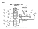
- FIG. 8A is a circuit diagram showing a second connection state of the high-frequency circuit 1A according to Modification 4.
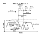
- FIG. 8B is a diagram showing an example of the frequency relationship of each communication band applied to the high-frequency circuit 1A according to Modification 4, and the pass characteristics of each filter in the second connection state.
- the high-frequency circuit 1A according to the fourth modification includes filters 11, 12, 13, 21, and 22, a switch 51, a matching circuit 75, power amplifiers 31, 33, and 41, low-noise amplifiers 32 and 42, antenna terminals 101 and 102, high-frequency input terminals 110, 130, and 150, and high-frequency output terminals 120 and 140.
- the high-frequency circuit 1A according to this modification differs from the high-frequency circuit 1 according to the embodiment in that a circuit element for transmitting signals of communication band D is added.
- a description of the configuration of the high-frequency circuit 1A according to this modification that is the same as that of the high-frequency circuit 1 according to the embodiment will be omitted, and the different configuration will be mainly described.
- Antenna terminal 101 is connected to antenna 2a and terminal 51a of switch 51.
- Antenna terminal 102 is connected to antenna 2b and terminal 51b of switch 51.
- High frequency input terminal 150 is connected to power amplifier 33 and is a terminal for receiving a transmission signal.
- communication band A is an example of a first communication band
- communication band B is an example of a second communication band
- communication band D is an example of a fourth communication band.
- Communication band A, communication band B, and communication band D are a band combination that allows simultaneous communication.
- the transmission band (A-Tx) of communication band A and the reception band (B-Rx) of communication band B partially overlap in frequency.
- the transmission band (D-Tx) of communication band D does not overlap in frequency with the transmission band (A-Tx) of communication band A and the reception band (B-Rx) of communication band B.
- the transmission band of communication band A is an example of a first frequency band
- the reception band of communication band B is an example of a second frequency band
- the transmission band of communication band D is an example of a third frequency band.
- the transmission band of communication band A includes subband X (first subband) that overlaps with the reception band of communication band B, and subband Y (second subband) that does not overlap with the reception band of communication band B.
- the reception band of communication band B includes subband X (first subband) that overlaps with the transmission band of communication band A, and subband Z (third subband) that does not overlap with the transmission band of communication band A.
- Filter 11 is an example of a first filter, and varies a first passband including subband X and subband Y, and a second passband including subband Y and narrower than the first passband. In other words, filter 11 varies a first characteristic having a first passband, and a second characteristic having a second passband.
- One end of filter 11 is connected to terminal 51c (first terminal) of switch 51 (first switch), and the other end of filter 11 is connected to the output terminal of power amplifier 31.
- Filter 22 is an example of a second filter, and has a passband that includes the reception band (second frequency band) of communication band B.
- One end of filter 22 is connected to terminal 51d (second terminal) of switch 51 (first switch), and the other end of filter 22 is connected to the input terminal of low-noise amplifier 42.
- the filter 12 has a pass band that includes the reception band of the communication band A.
- One end of the filter 12 is connected to the terminal 51c of the switch 51, and the other end of the filter 12 is connected to the input terminal of the low-noise amplifier 32.
- the filter 21 has a pass band that includes the transmission band of the communication band B. One end of the filter 21 is connected to the terminal 51d of the switch 51, and the other end of the filter 21 is connected to the output terminal of the power amplifier 41.
- Filter 13 is an example of a third filter, and has a passband that includes the transmission band (third frequency band) of communication band D.
- One end of filter 13 is connected to terminal 51c (first terminal) of switch 51 (first switch), and the other end of filter 13 is connected to the output terminal of power amplifier 33.
- Matching circuit 75 is an example of an impedance matching circuit, and is connected between terminal 51e and ground.
- Matching circuit 75 is composed of, for example, at least one of an inductor, a capacitor, and an elastic wave resonator.
- Switch 51 is an example of a first switch and a second switch, and has terminal 51a (first antenna connection terminal), terminal 51b (second antenna connection terminal), terminal 51c (first terminal), terminal 51d (second terminal), and terminal 51e.
- Terminals 51a, 51b, 51c, and 51d of switch 51 constitute a first switch
- terminals 51a and 51e of switch 51 constitute a second switch.
- Switch 51 switches between connection and non-connection between terminals 51a and 51c, between connection and non-connection between terminals 51a and 51d, between connection and non-connection between terminals 51b and 51c, and between connection and non-connection between terminals 51b and 51c, and between connection and non-connection between terminals 51b and 51d.
- Switch 51 also switches between connection and non-connection between terminals 51a and 51e.
- switch 51 may be a switch circuit composed of a first switch having terminals 51a, 51b, 51c, and 51d, and a second switch having terminals 51a and 51e.
- Terminal 51a is connected to antenna terminal 101
- terminal 51b is connected to antenna terminal 102
- terminal 51c is connected to filters 11, 12 and 13
- terminal 51d is connected to filters 21 and 22,
- terminal 51e is connected to matching circuit 75.
- switch 51 switches between connection and disconnection between antenna 2a and filters 11 to 13, between connection and disconnection between antenna 2a and filters 21 and 22, between connection and disconnection between antenna 2b and filters 11 to 13, between connection and disconnection between antenna 2b and filters 21 and 22, and between connection and disconnection between antenna 2a and matching circuit 75.
- switch 51 may switch between connection and disconnection between terminal 51c and terminal 51e. In this case, instead of switching between connecting and disconnecting the antenna 2a and the matching circuit 75, the switch 51 switches between connecting and disconnecting the filters 11 to 13 and the matching circuit 75.
- the output terminal of the power amplifier 33 is connected to the filter 13, and the input terminal is connected to the radio frequency input terminal 150.
- the power amplifier 33 amplifies the transmission signal of the communication band D input from the radio frequency input terminal 150.
- the high frequency circuit 1A can execute (1) a fifth mode in which a transmission signal of subband Y of communication band A, a reception signal of subband Z of communication band B, and a transmission signal of communication band D are simultaneously transmitted, (2) a sixth mode in which a transmission signal of communication band A and a transmission signal of communication band D are simultaneously transmitted, but a reception signal of communication band B is not transmitted, and (3) a third mode in which a reception signal of communication band B is transmitted, but a transmission signal of communication band A is not transmitted.
- the filter 11 is set to the first passband, so that the transmission signal of communication band A can be transmitted using the entire transmission band of communication band A.
- terminal 51a is connected to terminal 51c, and terminal 51d is not connected to terminals 51a and 51b. Furthermore, terminal 51a is not connected to terminal 51e.
- the filter 11 when the fifth mode is executed, the filter 11 is set to the second passband. At this time, terminals 51a and 51c are connected, and terminals 51b and 51d are connected. This improves the isolation between the transmission signal of communication band A that passes through filter 11 and the reception signal of communication band B that passes through filter 22, and suppresses deterioration of the reception sensitivity of communication band B.
- the passband of filter 11 is changed from the first passband to the second passband, and the attenuation characteristics of filter 11 in the transmission band of communication band D change (the attenuation characteristics are shown by the dashed line in Fig. 8B (matching circuit 75 not connected)).
- matching circuit 75 is connected to filters 11, 12, and 13 by further connecting terminals 51a and 51e. This makes it possible to adjust the attenuation characteristics of filter 11 when the passband changes, and improves the attenuation characteristics of filter 11 in the transmission band of communication band D (the attenuation characteristics are shown by the solid line in Fig. 8B (matching circuit 75 connected)).
- the communication band A is, for example, either band 8 for 4G-LTE or band n8 for 5G-NR
- the communication band B is, for example, either band 5 for 4G-LTE or band n5 for 5G-NR
- the communication band D is, for example, either band 28 (transmit band: 703-748MHz, receive band: 758-803MHz) and band 12 (transmit band: 699-716MHz, receive band: 729-746MHz) for 4G-LTE
- band n28 transmit band: 703-748MHz, receive band: 758-803MHz
- band n12 transmit band: 699-716MHz, receive band: 729-746MHz for 5G-NR.
- FIG. 9A is a circuit diagram of a high-frequency circuit 1B and a diver circuit 5B according to Modification 5.
- the high-frequency circuit 1B is an example of a high-frequency circuit according to the present invention, and is connected to the diver circuit 5B.
- the high-frequency circuit 1B according to this modification includes filters 11, 12, 13, 21, 22, and 23, a switch 52, and a matching circuit 75.
- Filter 11 is an example of a first filter and has a passband that includes the transmission band of band n8 (communication band A) for 5G-NR.
- Band n8 for 5G-NR is an example of a first communication band.
- Filter 12 has a passband that includes the reception band of band n8 for 5G-NR.
- Filter 21 has a passband that includes the transmission band of band n5 (communication band B) for 5G-NR and the transmission band of band n26 (transmission band: 814-849 MHz, reception band: 859-894 MHz).
- Band n5 for 5G-NR is an example of a second communication band.
- Filter 22 is an example of a second filter and has a passband that includes the reception band of band n5 and the reception band of band n26 for 5G-NR.
- Filter 13 has a passband that includes the transmission band of band n28 (communication band D) for 5G-NR or the transmission band of band n12 (communication band D) for 5G-NR.
- Filter 23 has a passband that includes the receiving band of band n28 for 5G-NR or the receiving band of band n12 for 5G-NR.
- band n8 and band n5 are a band combination that allows simultaneous communication.
- the transmission band of band n8 and the reception band of band n5 partially overlap in frequency.
- the transmission band of band n8 is an example of a first frequency band
- the reception band of band n5 is an example of a second frequency band.
- the transmission band of band n8 includes subband X (first subband) that overlaps with the reception band of band n5, and subband Y (second subband) that does not overlap with the reception band of band n5.
- the reception band of band n5 includes subband X (first subband) that overlaps with the transmission band of band n8, and subband Z (third subband) that does not overlap with the transmission band of band n8.
- Filter 11 varies between a first passband that includes subband X and subband Y, and a second passband that includes subband Y and is narrower than the first passband.
- One end of filter 11 is connected to a first selection terminal of switch 52.
- Filter 22 has a passband that includes subband X and subband Z. One end of filter 22 is connected to the second selection terminal of switch 52.
- Matching circuit 75 is an example of an impedance matching circuit, and is connected between the third selection terminal of switch 52 and ground.
- Switch 52 is an example of a first switch, and switches between the connection and disconnection of the first antenna and filters 11 and 12, between the connection and disconnection of the first antenna and filters 21 and 22, between the connection and disconnection of the first antenna and filters 13 and 23, between the connection and disconnection of the first antenna and diverter circuit 5B, between the connection and disconnection of the second antenna and filters 11 and 12, between the connection and disconnection of the second antenna and filters 21 and 22, between the connection and disconnection of the second antenna and filters 13 and 23, between the connection and disconnection of the second antenna and diverter circuit 5B, and between the connection and disconnection of the second antenna and matching circuit 75.
- the diver circuit 5B also includes filters 82 and 92 and a switch 53.
- Filter 92 has a passband that includes the reception band of band n5 and the reception band of band n26 for 5G-NR.
- Filter 82 has a passband that includes the receive band of band n8 for 5G-NR.
- the switch 53 switches between the connection and disconnection between the third antenna and the filter 92, between the connection and disconnection between the third antenna and the filter 82, between the connection and disconnection between the third antenna and the high-frequency circuit 1B, between the connection and disconnection between the fourth antenna and the filter 92, between the connection and disconnection between the fourth antenna and the filter 82, and between the connection and disconnection between the fourth antenna and the high-frequency circuit 1B.
- the high frequency circuit 1B and the diver circuit 5B can execute (1) a first mode in which a transmission signal of sub-band Y of communication band A and a reception signal of sub-band Z of communication band B are simultaneously transmitted, (2) a second mode in which a transmission signal of communication band A is transmitted but a reception signal of communication band B is not transmitted, and (3) a third mode in which a reception signal of communication band B is transmitted but a transmission signal of communication band A is not transmitted.
- the filter 11 when the second mode is executed, the filter 11 is set to the first passband, so that the transmission signal of the communication band A can be transmitted using the entire transmission band of the communication band A. Also, when the second mode is executed, the filter 11 is connected to the first antenna or the second antenna.
- the received signal of the communication band B can be transmitted using the filter 22.
- the filter 22 is connected to the first antenna or the second antenna.
- the filter 11 When the first mode is executed, the filter 11 is set to the second passband, and as shown in FIG. 9A, the filter 11 is connected to the second antenna, and the filter 22 is connected to the first antenna.
- the first antenna or the second antenna may also be connected to a matching circuit 75. This improves the isolation between the transmission signal of communication band A that passes through the filter 11 and the reception signal of communication band B that passes through the filter 22, and suppresses deterioration of the reception sensitivity of communication band B.
- the filter 82 may be connected to the fourth antenna, and the filter 92 may be connected to the third antenna. This allows the reception signal of communication band A and the reception signal of communication band B to be received by the diver circuit 5B.
- 9B is a circuit configuration diagram of a high-frequency circuit 1C and a primary circuit 5C according to Modification 6.
- the high-frequency circuit 1C is an example of a high-frequency circuit according to the present invention, and is connected to the primary circuit 5C.
- the high-frequency circuit 1C according to this modification includes filters 11, 12, 22, and 23, a switch 55, and a matching circuit 75.
- Filter 11 is an example of a first filter and has a passband that includes the transmission band of band n8 (communication band A) for 5G-NR.
- Band n8 for 5G-NR is an example of a first communication band.
- Filter 12 has a passband that includes the reception band of band n8 for 5G-NR.
- Filter 22 is an example of a second filter and has a passband that includes the reception band of band n5 (communication band B) for 5G-NR and the reception band of band n26.
- Filter 23 has a passband that includes the reception band of band n28 (communication band D) for 5G-NR or the reception band of band n12 for 5G-NR.
- band n8 and band n5 are a band combination that allows simultaneous communication.
- the transmission band of band n8 and the reception band of band n5 partially overlap in frequency.
- the transmission band of band n8 is an example of a first frequency band
- the reception band of band n5 is an example of a second frequency band.
- the transmission band of band n8 includes subband X (first subband) that overlaps with the reception band of band n5, and subband Y (second subband) that does not overlap with the reception band of band n5.
- the reception band of band n5 includes subband X (first subband) that overlaps with the transmission band of band n8, and subband Z (third subband) that does not overlap with the transmission band of band n8.
- Filter 11 varies between a first passband that includes subband X and subband Y, and a second passband that includes subband Y and is narrower than the first passband.
- One end of filter 11 is connected to a first selection terminal of switch 55.
- Filter 22 has a passband that includes subband X and subband Z. One end of filter 22 is connected to the second selection terminal of switch 55.
- the matching circuit 75 is an example of an impedance matching circuit, and is connected between the third selection terminal of the switch 55 and ground.
- Switch 55 is an example of a first switch, and switches between the connection and disconnection of the first antenna and filters 11 and 12, between the connection and disconnection of the first antenna and filter 22, between the connection and disconnection of the first antenna and filter 23, between the connection and disconnection of the first antenna and primary circuit 5C, between the connection and disconnection of the second antenna and filters 11 and 12, between the connection and disconnection of the second antenna and filter 22, between the connection and disconnection of the second antenna and filter 23, between the connection and disconnection of the second antenna and primary circuit 5C, and between the connection and disconnection of the second antenna and matching circuit 75.
- the primary circuit 5C includes filters 82, 83, 84, 91, and 92, and a switch 54.
- Filter 82 has a passband that includes the receive band of band n8 for 5G-NR.
- Filter 83 has a passband that includes the transmission band of band n28 for 5G-NR or the transmission band of band n12 for 5G-NR.
- Filter 84 has a passband that includes the receiving band of band n28 for 5G-NR or the receiving band of band n12 for 5G-NR.
- Filter 91 has a passband that includes the transmission band of band n5 and the transmission band of band n26 for 5G-NR.
- Filter 92 has a passband that includes the reception band of band n5 and the reception band of band n26 for 5G-NR.
- Switch 54 switches between connection and disconnection between the third antenna and filter 82, between connection and disconnection between the third antenna and filters 83 and 84, between connection and disconnection between the third antenna and filters 91 and 92, between connection and disconnection between the third antenna and high-frequency circuit 1C, between connection and disconnection between the fourth antenna and filter 82, between connection and disconnection between the fourth antenna and filters 83 and 84, between connection and disconnection between the fourth antenna and filters 91 and 92, and between connection and disconnection between the fourth antenna and high-frequency circuit 1C.
- the high-frequency circuit 1C and the primary circuit 5C can execute (1) a first mode in which a transmission signal of subband Y of communication band A and a reception signal of subband Z of communication band B are simultaneously transmitted, (2) a second mode in which a transmission signal of communication band A is transmitted but a reception signal of communication band B is not transmitted, and (3) a third mode in which a reception signal of communication band B is transmitted but a transmission signal of communication band A is not transmitted.
- the filter 11 when the second mode is executed, the filter 11 is set to the first passband, so that the transmission signal of the communication band A can be transmitted using the entire transmission band of the communication band A. Also, when the second mode is executed, the filter 11 is connected to the first antenna or the second antenna.
- the received signal of the communication band B can be transmitted using the filter 22.
- the filter 22 is connected to the first antenna or the second antenna.
- filter 11 When the first mode is executed, filter 11 is set to the second passband, and as shown in FIG. 9B, filter 11 is connected to the second antenna, and filter 22 is connected to the first antenna. Also, the first antenna or the second antenna may be connected to matching circuit 75. This improves the isolation between the transmission signal of communication band A that passes through filter 11 and the reception signal of communication band B that passes through filter 22, and suppresses deterioration of the reception sensitivity of communication band B.
- filter 82 may be connected to the fourth antenna, and filters 91 and 92 may be connected to the third antenna. This allows the received signal of communication band A and the received signal of communication band B to be transmitted simultaneously by primary circuit 5C.
- the high-frequency circuit 1 includes the filter 11 having a pass band including a first frequency band which is one of the transmission band and reception band of the communication band A, and the filter 22 having a pass band including a second frequency band which is the other of the transmission band and reception band of the communication band B, the communication band A and the communication band B are a band combination enabling simultaneous communication, the first frequency band includes a sub-band X which overlaps with the second frequency band and a sub-band Y which does not overlap with the second frequency band, the second frequency band includes sub-band X and a sub-band Z which does not overlap with the first frequency band, and the pass band of the filter 11 is variable to a first pass band which includes sub-band X and sub-band Y, and a second pass band which includes sub-band Y and is narrower than the first pass band.
- the signal when a signal in the first frequency band is transmitted alone, the signal can be transmitted using the entire bandwidth of the first frequency band by setting filter 11 to the first passband.
- the isolation between the two signals can be improved by setting filter 11 to the second passband, so that deterioration of reception sensitivity when signals in subband Y and signals in subband Z are transmitted simultaneously can be suppressed.
- a small-sized high-frequency circuit 1 can be provided that can simultaneously transmit signals in communication band A and communication band B while suppressing deterioration of isolation and reception sensitivity.
- the passband of the filter 11 becomes the first passband, and when the first frequency band signal and the second frequency band signal are transmitted simultaneously, the passband of the filter 11 becomes the second passband.
- the first frequency band is the transmission band of communication band A
- the second frequency band is the reception band of communication band B.
- the transmission signal when a transmission signal of communication band A is transmitted alone, the transmission signal can be transmitted using the entire bandwidth of the transmission band of communication band A by setting filter 11 to the first pass band.
- a transmission signal of communication band A when a transmission signal of communication band A is passed through filter 11 and a reception signal of communication band B is passed through filter 22 for simultaneous transmission, even if filter 11 and filter 22 are arranged close to each other, isolation between the two signals can be improved by setting filter 11 to the second pass band, so that deterioration of reception sensitivity can be suppressed when a transmission signal of communication band A and a reception signal of communication band B are transmitted simultaneously. Therefore, a small-sized high-frequency circuit 1 can be provided that can simultaneously transmit a transmission signal of communication band A and a reception signal of communication band B while suppressing deterioration of isolation and reception sensitivity.
- the first frequency band is the receiving band of communication band B
- the second frequency band is the transmitting band of communication band A
- filter 22 varies between a first passband that includes subband X and subband Z, and a second passband that includes subband Z and is narrower than the first passband.
- the received signal of communication band B when the received signal of communication band B is transmitted alone, the received signal can be transmitted using the entire bandwidth of the received band of communication band B by setting filter 22 to the first passband.
- the received signal of communication band B when the received signal of communication band B is passed through filter 22 and the transmitted signal of communication band A is passed through filter 11 for simultaneous transmission, the isolation of both signals can be improved by setting filter 22 to the second passband, thereby suppressing deterioration of the receiving sensitivity of communication band B when transmitted simultaneously.
- subband Y overlaps with at least one of the transmission band and reception band of communication band C
- subband X does not overlap with at least one of the transmission band and reception band of communication band C
- the passband of filter 11 becomes the second passband
- the quality of the signal of communication band C passing through filter 11 can be improved by setting filter 11 to the second passband.
- communication band C is band n106 for 5G-NR.
- filter 11 varies a first passband including subband X and subband Y and a second passband including subband Y and narrower than the first passband
- filter 22 varies a third passband including subband X and subband Z and a fourth passband including subband Z and narrower than the third passband.
- the passbands of filters 11 and 22 are variable, so that even if filters 11 and 22 are placed close to each other, isolation between signals in communication band A and signals in communication band B can be ensured. This makes it possible to suppress deterioration of reception sensitivity when signals in subband Y and subband Z are transmitted simultaneously.
- the passband of filter 11 when only the first frequency band signal of the first frequency band signal and the second frequency band signal is transmitted, the passband of filter 11 is the first passband, when only the second frequency band signal of the first frequency band signal and the second frequency band signal is transmitted, the passband of filter 22 is the third passband, and when the first frequency band signal and the second frequency band signal are transmitted simultaneously, the passband of filter 11 is the second passband and the passband of filter 22 is the fourth passband.
- the high frequency circuit 1 further includes a switch 50 having a terminal 50a connected to an antenna, a terminal 50b connected to an antenna, a terminal 50c connected to the filter 11, and a terminal 50d connected to the filter 22.
- the terminal 50c when transmitting only the first frequency band signal out of the first frequency band signal and the second frequency band signal, the terminal 50c is connected to the terminal 50a and the terminal 50d is connected to neither the terminal 50a nor the terminal 50b, and when transmitting the first frequency band signal and the second frequency band signal simultaneously, the terminal 50c is connected to the terminal 50a and the terminal 50d is connected to the terminal 50b.
- the high-frequency circuit 1A according to the fourth modification further includes a filter 13 connected to the terminal 51c and having a passband including a third frequency band, which is one of the transmission band and reception band of the communication band D, a matching circuit 75, and a switch 51 for switching between connection and disconnection between the terminal 51c and the matching circuit 75, and the third frequency band does not overlap with the first frequency band and the second frequency band.
- the high frequency circuit 1A can execute (1) a fifth mode in which signals of communication band A, communication band B, and communication band D are transmitted simultaneously, (2) a sixth mode in which signals of communication band A and communication band D are transmitted simultaneously, but signals of communication band B are not transmitted, and (3) a third mode in which signals of communication band B are transmitted, but signals of communication band A are not transmitted.
- the matching circuit 75 can be switched between connected and disconnected when switching between modes, making it possible to improve the attenuation characteristics of the filter 11 in the communication band D.
- terminal 51c when transmitting only the first frequency band signal out of the first frequency band signal and the second frequency band signal, terminal 51c is connected to terminal 51a, terminal 51d is connected to neither terminal 51a nor 51b, and matching circuit 75 is connected to terminals 51c and 51e, whereas when transmitting the first frequency band signal and the second frequency band signal simultaneously, terminal 51c is connected to terminal 51a, terminal 51d is connected to terminal 51b, and matching circuit 75 is connected to terminal 51c.
- the passband of the filter 11 When switching from the sixth mode to the fifth mode, the passband of the filter 11 is changed from the first passband to the second passband, thereby changing the attenuation characteristics of the filter 11 in the communication band D.
- a matching circuit 75 when switching to the fifth mode, by further connecting a matching circuit 75 to the filter 11, it is possible to adjust the attenuation characteristics of the filter 11 when the passband is changed, and to improve the attenuation characteristics of the filter 11 in the communication band D. Therefore, in the simultaneous transmission of signals of two communication bands A and B, which have partially overlapping frequency bands, it is possible to suppress deterioration of isolation and receiving sensitivity, and it is possible to transmit the communication band D, which is transmitted simultaneously with the communication bands A and B, with low loss.
- the communication band D is either band 28 or band 12 for 4G-LTE, or band n28 or band n12 for 5G-NR.
- a first switch of the SPDT type is provided that has an antenna connection terminal, a first terminal connected to the filter 11, and a second terminal connected to the filter 22.
- the first terminal when transmitting only the first frequency band signal out of the first frequency band signal and the second frequency band signal, the first terminal is connected to the antenna connection terminal and the second terminal is not connected to the antenna connection terminal, and when transmitting the first frequency band signal and the second frequency band signal simultaneously, the first terminal is connected to the antenna connection terminal and the second terminal is connected to the antenna connection terminal.
- the communication band A is either band 8 for 4G-LTE or band n8 for 5G-NR
- the communication band B is either band 5 for 4G-LTE or band n5 for 5G-NR.
- the communication device 4 also includes an RFIC 3 that processes high-frequency signals, and a high-frequency circuit 1 that transmits high-frequency signals between the RFIC 3 and the antennas 2a and 2b.
- the effects of the high-frequency circuit 1 can be realized in the communication device 4.
- the high-frequency circuit and communication device according to the present invention have been described above based on the embodiments and modifications, the high-frequency circuit and communication device according to the present invention are not limited to the above-mentioned embodiments and modifications.
- the present invention also includes other embodiments realized by combining any of the components in the above-mentioned embodiments and modifications, modifications obtained by applying various modifications to the above-mentioned embodiments and modifications that would come to mind by a person skilled in the art without departing from the spirit of the present invention, and various devices incorporating the above-mentioned high-frequency circuit and communication device.
- circuit elements and wiring etc. may be inserted between the paths connecting the circuit elements and signal paths shown in the drawings.
- a cellular band for 5G-NR or LTE is used, but a communication band for another radio access technology may be used in addition to or instead of 5G-NR or LTE.
- a communication band for a wireless local area network may be used.
- a first filter having a passband that includes a first frequency band, the first frequency band being one of a transmit band and a receive band of a first communications band; a second filter having a passband that includes a second frequency band that is the other of the transmission band and the reception band of the second communications band; the first communication band and the second communication band are a band combination capable of simultaneous communication, the first frequency band includes a first sub-band that overlaps with the second frequency band and a second sub-band that does not overlap with the second frequency band; the second frequency band includes the first sub-band and a third sub-band that does not overlap with the first communications band;
- a high-frequency circuit wherein the passband of the first filter is variable to a first passband including the first subband and the second subband, and a second passband including the second subband and narrower than the first passband.
- the pass band of the first filter is the first pass band
- the first frequency band is a transmission band of the first communications band;
- the first frequency band is a reception band of the first communication band;
- the second subband overlaps with at least one of a transmission band and a reception band of a third communications band; the first sub-band does not overlap with at least one of a transmission band and a reception band of the third communications band;
- the high-frequency circuit according to any one of ⁇ 1> to ⁇ 4>, wherein, when transmitting at least one signal of a transmission band and a reception band of the third communication band, a pass band of the first filter becomes the second pass band.
- ⁇ 6> The high-frequency circuit according to ⁇ 5>, wherein the third communication band is band n106 for 5G-NR.
- ⁇ 7> The high-frequency circuit according to any one of ⁇ 1> to ⁇ 6>, wherein the second filter varies a third passband including the first subband and the third subband, and a fourth passband including the third subband and narrower than the third passband.
- ⁇ 8> When transmitting only the first frequency band signal of the first frequency band signal and the second frequency band signal, the pass band of the first filter becomes the first pass band, When transmitting only the second frequency band signal of the first frequency band signal and the second frequency band signal, the pass band of the second filter becomes the third pass band,
- the high-frequency circuit according to ⁇ 7> wherein, when a signal of the first frequency band and a signal of the second frequency band are simultaneously transmitted, a pass band of the first filter is the second pass band, and a pass band of the second filter is the fourth pass band.
- the high-frequency circuit according to any one of ⁇ 1> to ⁇ 8>, comprising a first switch having a first antenna connecting terminal, a second antenna connecting terminal, a first terminal connected to the first filter, and a second terminal connected to the second filter.
- ⁇ 10> when transmitting only the first frequency band signal of the first frequency band signal and the second frequency band signal, the first terminal is connected to one of the first antenna connecting terminal and the second antenna connecting terminal, and the second terminal is connected to neither the first antenna connecting terminal nor the second antenna connecting terminal,
- the high-frequency circuit according to ⁇ 9> wherein, when a signal of the first frequency band and a signal of the second frequency band are simultaneously transmitted, the first terminal is connected to the first antenna connection terminal or the second antenna connection terminal, and the second terminal is connected to the first antenna connection terminal or the second antenna connection terminal.
- a third filter connected to the first terminal and having a passband that includes a third frequency band, the third frequency band being one of a transmit band and a receive band of a fourth communications band;
- An impedance matching circuit An impedance matching circuit; a second switch that switches between connection and disconnection between the first terminal and the impedance matching circuit, The high-frequency circuit according to ⁇ 9> or ⁇ 10>, wherein the third frequency band does not overlap with the first frequency band and the second frequency band.
- ⁇ 12> when transmitting only the first frequency band signal of the first frequency band signal and the second frequency band signal, the first terminal is connected to one of the first antenna connecting terminal and the second antenna connecting terminal, the second terminal is connected to neither the first antenna connecting terminal nor the second antenna connecting terminal, and the impedance matching circuit is not connected to the first terminal,
- the high-frequency circuit according to ⁇ 11> wherein, when a signal in the first frequency band and a signal in the second frequency band are simultaneously transmitted, the first terminal is connected to the first antenna connection terminal or the second antenna connection terminal, the second terminal is connected to the first antenna connection terminal or the second antenna connection terminal, and the impedance matching circuit is connected to the first terminal.
- the fourth communication band is any one of band 28 and band 12 for 4G-LTE, and band n28 and band n12 for 5G-NR.
- the high-frequency circuit according to any one of ⁇ 1> to ⁇ 8> further comprising a first switch having an antenna connection terminal, a first terminal connected to the first filter, and a second terminal connected to the second filter.
- ⁇ 15> When transmitting only the first frequency band signal among the first frequency band signal and the second frequency band signal, the first terminal is connected to the antenna connection terminal and the second terminal is not connected to the antenna connection terminal;
- the high-frequency circuit according to ⁇ 14> wherein, when a signal of the first frequency band and a signal of the second frequency band are simultaneously transmitted, the first terminal is connected to the antenna connection terminal, and the second terminal is connected to the antenna connection terminal.
- a third filter connected to the first terminal and having a passband that includes a third frequency band, the third frequency band being one of a transmit band and a receive band of a fourth communications band;
- An impedance matching circuit An impedance matching circuit; a second switch that switches between connection and disconnection between the first terminal and the impedance matching circuit, The high-frequency circuit according to ⁇ 14> or ⁇ 15>, wherein the third frequency band does not overlap with the first frequency band and the second frequency band.
- ⁇ 17> when transmitting only the first frequency band signal of the first frequency band signal and the second frequency band signal, the first terminal is connected to the antenna connection terminal, the second terminal is not connected to the antenna connection terminal, and the impedance matching circuit is not connected to the first terminal;
- the high-frequency circuit according to ⁇ 16> wherein, when a signal in the first frequency band and a signal in the second frequency band are simultaneously transmitted, the first terminal is connected to the antenna connection terminal, the second terminal is connected to the antenna connection terminal, and the impedance matching circuit is connected to the first terminal.
- the fourth communication band is any one of band 28 and band 12 for 4G-LTE, and band n28 and band n12 for 5G-NR.
- the first communication band is either band 8 for 4G-LTE or band n8 for 5G-NR;
- the radio frequency circuit according to any one of ⁇ 1> to ⁇ 18>, wherein the second communication band is either band 5 for 4G-LTE or band n5 for 5G-NR.
- a signal processing circuit for processing a high frequency signal A communication device comprising: a high-frequency circuit according to any one of ⁇ 1> to ⁇ 19>, which transmits the high-frequency signal between the signal processing circuit and an antenna.
- the present invention can be widely used as a high-frequency circuit placed in the front end of communication devices such as mobile phones.
Landscapes
- Engineering & Computer Science (AREA)
- Computer Networks & Wireless Communication (AREA)
- Signal Processing (AREA)
- Transceivers (AREA)
Abstract
Description
本発明は、高周波回路および通信装置に関する。 The present invention relates to high-frequency circuits and communication devices.
マルチバンドに対応したフロントエンド回路に対して、複数の高周波信号を低損失かつ高アイソレーションで送受信することが求められている。 Multiband front-end circuits are required to transmit and receive multiple high-frequency signals with low loss and high isolation.
特許文献1には、通過帯域の異なる複数のフィルタがマルチプレクサ(スイッチ)を介してアンテナに接続された構成を有する高周波モジュール(高周波回路)が開示されている。
3GPP(登録商標)(3rd Generation Partnership Project)では、周波数帯域が一部重複する2つの通信バンドの信号の同時伝送が検討されている。 3GPP (registered trademark) (3rd Generation Partnership Project) is considering simultaneous transmission of signals in two communication bands with partially overlapping frequency bands.
本発明は、周波数帯域が一部重複する2つの通信バンドの信号の同時伝送を、アイソレーションおよび受信感度の劣化を抑制して実行できる小型の高周波回路および通信装置を提供することを目的とする。 The present invention aims to provide a small high-frequency circuit and communication device that can simultaneously transmit signals in two communication bands with partially overlapping frequency bands while minimizing degradation of isolation and reception sensitivity.
上記目的を達成するために、本発明の一態様に係る高周波回路は、第1通信バンドの送信バンドおよび受信バンドの一方である第1周波数バンドを含む通過帯域を有する第1フィルタと、第2通信バンドの送信バンドおよび受信バンドの他方である第2周波数バンドを含む通過帯域を有する第2フィルタと、を備え、第1通信バンドと第2通信バンドとは、同時通信可能なバンドコンビネーションであり、第1周波数バンドは、第2周波数バンドと重複する第1サブバンド、および、第2周波数バンドと重複しない第2サブバンドを含み、第2周波数バンドは、第1サブバンド、および、第1通信バンドと重複しない第3サブバンドを含み、第1フィルタの通過帯域は、第1サブバンドおよび第2サブバンドを含む第1通過帯域、および、第2サブバンドを含み第1通過帯域よりも狭い第2通過帯域に可変である。 In order to achieve the above object, a high-frequency circuit according to one embodiment of the present invention comprises a first filter having a passband including a first frequency band, which is one of the transmission band and reception band of a first communication band, and a second filter having a passband including a second frequency band, which is the other of the transmission band and reception band of a second communication band, the first communication band and the second communication band being a band combination capable of simultaneous communication, the first frequency band including a first subband that overlaps with the second frequency band and a second subband that does not overlap with the second frequency band, the second frequency band including the first subband and a third subband that does not overlap with the first communication band, and the passband of the first filter is variable to a first passband including the first subband and the second subband, and a second passband including the second subband and narrower than the first passband.
本発明によれば、周波数帯域が一部重複する2つの通信バンドの信号の同時伝送を、アイソレーションおよび受信感度の劣化を抑制して実行できる小型の高周波回路および通信装置を提供することが可能となる。 The present invention makes it possible to provide a small high-frequency circuit and communication device that can simultaneously transmit signals in two communication bands with partially overlapping frequency bands while minimizing degradation of isolation and reception sensitivity.
以下、本発明の実施の形態について、図面を用いて詳細に説明する。なお、以下で説明する実施の形態は、いずれも包括的または具体的な例を示すものである。以下の実施の形態で示される数値、形状、材料、構成要素、構成要素の配置および接続形態などは、一例であり、本発明を限定する主旨ではない。 Below, the embodiments of the present invention will be described in detail with reference to the drawings. Note that the embodiments described below are all comprehensive or specific examples. The numerical values, shapes, materials, components, arrangements and connection forms of the components shown in the following embodiments are merely examples and are not intended to limit the present invention.
なお、各図は、本発明を示すために適宜強調、省略、または比率の調整を行った模式図であり、必ずしも厳密に図示されたものではなく、実際の形状、位置関係、および比率とは異なる場合がある。各図において、実質的に同一の構成に対しては同一の符号を付しており、重複する説明は省略または簡素化される場合がある。 Note that each figure is a schematic diagram in which emphasis, omissions, or adjustments to the ratio have been made as appropriate to illustrate the present invention, and is not necessarily an exact illustration, and may differ from the actual shape, positional relationship, and ratio. In each figure, the same reference numerals are used for substantially the same configuration, and duplicate explanations may be omitted or simplified.
本開示において、「接続される」とは、接続端子および/または配線導体で直接接続される場合だけでなく、他の回路素子を介して電気的に接続される場合も含むことを意味する。また、「AとBとの間に接続される」とは、AおよびBを結ぶ経路上でAおよびBと接続されることを意味する。 In this disclosure, "connected" refers not only to direct connection by a connection terminal and/or wiring conductor, but also to electrical connection via other circuit elements. Additionally, "connected between A and B" refers to connection to A and B on the path connecting A and B.
また、本開示において、「送信経路」とは、高周波送信信号が伝搬する配線、当該配線に直接接続された電極、および当該配線または当該電極に直接接続された端子等で構成された伝送線路であることを意味する。また、「受信経路」とは、高周波受信信号が伝搬する配線、当該配線に直接接続された電極、および当該配線または当該電極に直接接続された端子等で構成された伝送線路であることを意味する。 In addition, in this disclosure, a "transmission path" refers to a transmission line that is composed of a wiring through which a high-frequency transmission signal propagates, an electrode directly connected to the wiring, and a terminal directly connected to the wiring or the electrode. Also, a "reception path" refers to a transmission line that is composed of a wiring through which a high-frequency reception signal propagates, an electrode directly connected to the wiring, and a terminal directly connected to the wiring or the electrode.
また、本開示において、フィルタの通過帯域は、当該通過帯域内における挿入損失の最小値から3dB大きい2つの周波数間の周波数帯域と定義される。 Furthermore, in this disclosure, the passband of a filter is defined as the frequency band between two frequencies that are 3 dB greater than the minimum insertion loss within the passband.
(実施の形態)
[1 高周波回路1および通信装置4の回路構成]
本実施の形態に係る高周波回路1および通信装置4の回路構成について、図1を参照しながら説明する。図1は、実施の形態に係る高周波回路1および通信装置4の回路構成図である。
(Embodiment)
[1. Circuit configuration of
The circuit configuration of a high-
[1.1 通信装置4の回路構成]
まず、通信装置4の回路構成について説明する。図1に示すように、本実施の形態に係る通信装置4は、高周波回路1と、アンテナ2aおよび2bと、RF信号処理回路(RFIC)3と、を備える。
[1.1 Circuit configuration of communication device 4]
First, a description will be given of the circuit configuration of the
高周波回路1は、アンテナ2aおよび2bとRFIC3との間で高周波信号を伝送する。高周波回路1の詳細な回路構成については後述する。
The high-
アンテナ2aは、高周波回路1のアンテナ端子101に接続され、高周波回路1から出力された高周波信号を送信し、また、外部から高周波信号を受信して高周波回路1へ出力する。アンテナ2bは、高周波回路1のアンテナ端子102に接続され、高周波回路1から出力された高周波信号を送信し、また、外部から高周波信号を受信して高周波回路1へ出力する。
RFIC3は、高周波信号を処理する信号処理回路の一例である。具体的には、RFIC3は、高周波回路1の受信経路を介して入力された高周波受信信号を、ダウンコンバート等により信号処理し、当該信号処理して生成された受信信号をベースバンド信号処理回路(BBIC:図示せず)へ出力する。また、RFIC3は、BBICから入力された送信信号をアップコンバート等により信号処理し、当該信号処理して生成された高周波送信信号を、高周波回路1の送信経路に出力する。また、RFIC3は、高周波回路1が有するスイッチおよび増幅器等を制御する制御部を有する。なお、RFIC3の制御部としての機能の一部または全部は、RFIC3の外部に実装されてもよく、例えば、BBICまたは高周波回路1に実装されてもよい。
The RFIC3 is an example of a signal processing circuit that processes high-frequency signals. Specifically, the RFIC3 processes the high-frequency received signal input via the receiving path of the high-
なお、本実施の形態に係る通信装置4において、アンテナ2aおよび2bは、必須の構成要素ではない。
In addition,
[1.2 高周波回路1の回路構成]
次に、高周波回路1の回路構成について説明する。図1に示すように、高周波回路1は、フィルタ11、12、21および22と、スイッチ50と、電力増幅器31および41と、低雑音増幅器32および42と、アンテナ端子101および102と、高周波入力端子110および130と、高周波出力端子120および140と、を備える。
[1.2 Circuit configuration of high-frequency circuit 1]
Next, a description will be given of the circuit configuration of the high-
アンテナ端子101は、アンテナ2aおよびスイッチ50の端子50aに接続される。アンテナ端子102は、アンテナ2bおよびスイッチ50の端子50bに接続される。高周波入力端子110は、RFIC3および電力増幅器31に接続され、RFIC3から高周波送信信号を受けるための端子である。高周波入力端子130は、RFIC3および電力増幅器41に接続され、RFIC3から高周波送信信号を受けるための端子である。高周波出力端子120は、RFIC3および低雑音増幅器32に接続され、RFIC3に高周波受信信号を出力するための端子である。高周波出力端子140は、RFIC3および低雑音増幅器42に接続され、RFIC3に高周波受信信号を出力するための端子である。
The
図2は、実施の形態に係る高周波回路1に適用される通信バンドAおよび通信バンドBの周波数関係、および、フィルタ11および22の通過特性を例示した図である。
FIG. 2 illustrates the frequency relationship between communication band A and communication band B applied to high-
本実施の形態において、通信バンドAは第1通信バンドの一例であり、通信バンドBは第2通信バンドの一例である。通信バンドAと通信バンドBとは同時通信可能なバンドコンビネーションである。図2に示すように、通信バンドAの送信バンド(A-Tx)と通信バンドBの受信バンド(B-Rx)とは、周波数が一部重複している。 In this embodiment, communication band A is an example of a first communication band, and communication band B is an example of a second communication band. Communication band A and communication band B are a band combination that allows simultaneous communication. As shown in FIG. 2, the transmission band (A-Tx) of communication band A and the reception band (B-Rx) of communication band B partially overlap in frequency.
また、本実施の形態において、通信バンドAの送信バンドは、第1周波数バンドの一例であり、通信バンドBの受信バンドは、第2周波数バンドの一例である。図2に示すように、通信バンドAの送信バンドは、通信バンドBの受信バンドと重複するサブバンドX(第1サブバンド)、および、通信バンドBの受信バンドと重複しないサブバンドY(第2サブバンド)を含む。また、通信バンドBの受信バンドは、通信バンドAの送信バンドと重複するサブバンドX(第1サブバンド)、および、通信バンドAの送信バンドと重複しないサブバンドZ(第3サブバンド)を含む。 In addition, in this embodiment, the transmission band of communication band A is an example of a first frequency band, and the reception band of communication band B is an example of a second frequency band. As shown in FIG. 2, the transmission band of communication band A includes subband X (first subband) that overlaps with the reception band of communication band B, and subband Y (second subband) that does not overlap with the reception band of communication band B. Furthermore, the reception band of communication band B includes subband X (first subband) that overlaps with the transmission band of communication band A, and subband Z (third subband) that does not overlap with the transmission band of communication band A.
なお、本開示において、一のバンドと他のバンドとが一部重複する、とは、一のバンドのうちの一部の周波数範囲と他のバンドのうちの一部の周波数範囲とが重複することだけではなく、一のバンドの低周波端または高周波端の一点と、他のバンドの高周波端または低周波端の一点とが一致し、その他の周波数では一致しないことを含むものとする。 In this disclosure, "one band partially overlaps with another band" does not only mean that a portion of the frequency range of one band overlaps with a portion of the frequency range of the other band, but also means that a point at the low frequency end or high frequency end of one band coincides with a point at the high frequency end or low frequency end of the other band, but does not coincide at other frequencies.
すなわち、本実施の形態において、サブバンドXは所定の周波数一点のみで構成されてもよい。 In other words, in this embodiment, subband X may be composed of only one predetermined frequency point.
なお、本開示において、通信バンドA、通信バンドB、後述する通信バンドCおよび通信バンドDのそれぞれは、無線アクセス技術(RAT:Radio Access Technology)を用いて構築される通信システムのために、標準化団体など(例えば3GPP(登録商標)、IEEE(Institute of Electrical and Electronics Engineers)等)によって予め定義された周波数バンドを意味する。通信システムとしては、例えばLTE(Long Term Evolution)システム、5G(5th Generation)-NR(New Radio)システム、およびWLAN(Wireless Local Area Network)システム等を用いることができるが、これらに限定されない。 In this disclosure, each of communication band A, communication band B, and communication band C and communication band D described below means a frequency band predefined by a standardization organization (e.g., 3GPP (registered trademark), IEEE (Institute of Electrical and Electronics Engineers), etc.) for a communication system constructed using radio access technology (RAT). Examples of communication systems that can be used include, but are not limited to, an LTE (Long Term Evolution) system, a 5G (5th Generation)-NR (New Radio) system, and a WLAN (Wireless Local Area Network) system.
フィルタ11は、第1フィルタの一例であり、通信バンドAの送信バンド(第1周波数バンド)を含む通過帯域を有する。より具体的には、フィルタ11の通過帯域は、サブバンドXおよびサブバンドYを含む第1通過帯域、および、サブバンドYを含み第1通過帯域よりも狭い第2通過帯域に可変である。言い換えると、フィルタ11は、例えばRFIC3から出力される制御信号により、第1通過帯域を有する第1特性と、第2通過帯域を有する第2特性とを可変する。フィルタ11の一端はスイッチ50(第1スイッチ)の端子50c(第1端子)に接続され、フィルタ11の他端は電力増幅器31の出力端に接続される。
フィルタ22は、第2フィルタの一例であり、通信バンドBの受信バンド(第2周波数バンド)を含む通過帯域を有する。フィルタ22の一端はスイッチ50(第1スイッチ)の端子50d(第2端子)に接続され、フィルタ22の他端は低雑音増幅器42の入力端に接続される。
フィルタ12は、通信バンドAの受信バンドを含む通過帯域を有する。フィルタ12の一端はスイッチ50の端子50cに接続され、フィルタ12の他端は低雑音増幅器32の入力端に接続される。
The
フィルタ21は、通信バンドBの送信バンドを含む通過帯域を有する。フィルタ21の一端はスイッチ50の端子50dに接続され、フィルタ21の他端は電力増幅器41の出力端に接続される。
The
スイッチ50は、第1スイッチの一例であり、端子50a(第1アンテナ接続端子)、端子50b(第2アンテナ接続端子)、端子50c(第1端子)および端子50d(第2端子)を有する。スイッチ50は、DPDT(Double Pole Double Throw)型スイッチであり、端子50aと端子50cとの接続および非接続を切り替え、端子50aと端子50dとの接続および非接続を切り替え、端子50bと端子50cとの接続および非接続を切り替え、端子50bと端子50dとの接続および非接続を切り替える。端子50aはアンテナ端子101に接続され、端子50bはアンテナ端子102に接続され、端子50cはフィルタ11および12に接続され、端子50dはフィルタ21および22に接続される。上記接続構成により、スイッチ50は、アンテナ2aとフィルタ11および12との接続および非接続を切り替え、アンテナ2aとフィルタ21および22との接続および非接続を切り替え、アンテナ2bとフィルタ11および12との接続および非接続を切り替え、アンテナ2bとフィルタ21および22との接続および非接続を切り替える。
電力増幅器31は、出力端がフィルタ11に接続され、入力端が高周波入力端子110に接続される。電力増幅器31は、高周波入力端子110から入力された通信バンドAの高周波送信信号(以下、送信信号と記す)を増幅する。
The
電力増幅器41は、出力端がフィルタ21に接続され、入力端が高周波入力端子130に接続される。電力増幅器41は、高周波入力端子130から入力された通信バンドBの送信信号を増幅する。
The output terminal of the
低雑音増幅器32は、入力端がフィルタ12に接続され、出力端が高周波出力端子120に接続される。低雑音増幅器32は、アンテナ端子101または102から入力された通信バンドAの高周波受信信号(以下、受信信号と記す)を増幅する。
The input terminal of the low-
低雑音増幅器42は、入力端がフィルタ22に接続され、出力端が高周波出力端子140に接続される。低雑音増幅器42は、アンテナ端子101または102から入力された通信バンドBの受信信号を増幅する。
The input terminal of the
上記構成において、高周波回路1は、(1)通信バンドAのサブバンドYの送信信号と通信バンドBのサブバンドZの受信信号とを同時伝送する第1モード、(2)通信バンドAの送信信号を伝送し、通信バンドBの受信信号を伝送しない第2モード、および(3)通信バンドBの受信信号を伝送し、通信バンドAの送信信号を伝送しない第3モード、を実行できる。
In the above configuration, the
図3Aは、実施の形態に係る高周波回路1において通信バンドAの信号を単独伝送する場合のスイッチ50の接続状態を示す回路図である。図3Bは、実施の形態に係る高周波回路1において通信バンドAの送信信号および通信バンドBの受信信号を同時伝送する場合のスイッチ50の接続状態を示す回路図である。
FIG. 3A is a circuit diagram showing the connection state of the
上記構成において、第2モードを実行する場合には、フィルタ11を第1通過帯域に設定することで、通信バンドAの送信バンドの全域を用いて通信バンドAの送信信号を伝送できる。また、第2モードを実行する場合には、図3Aに示すように、スイッチ50の端子50aと端子50cとを接続する。さらに、第2モードを実行する場合には、スイッチ50の端子50bと端子50dとを非接続とすることが望ましい。これにより、フィルタ11を通過する通信バンドAの送信信号を、低損失で伝送できる。
In the above configuration, when the second mode is executed, the
また、第3モードを実行する場合には、フィルタ22を用いて通信バンドBの受信信号を伝送できる。また、第3モードを実行する場合には、スイッチ50の端子50bと端子50dとを接続する。さらに、第3モードを実行する場合には、スイッチ50の端子50aと端子50cとを非接続とすることが望ましい。これにより、フィルタ22を通過する通信バンドBの受信信号を、低損失で伝送できる。
Furthermore, when the third mode is executed, the received signal of communication band B can be transmitted using
また、第1モードを実行する場合には、フィルタ11を第2通過帯域に設定し、図3Bに示すように、スイッチ50の端子50aと端子50cとを接続し、端子50bと端子50dとを接続する。これにより、フィルタ11を通過する通信バンドAの送信信号とフィルタ22を通過する通信バンドBの受信信号とのアイソレーションを向上でき、通信バンドBの受信感度の劣化を抑制できる。
When the first mode is executed, the
なお、第1モードを実行する従来の構成の第一例としては、一部重複する通信バンドAの送信バンドおよび通信バンドBの受信バンドを包含する通過帯域を有する、いわゆる1つのコバンドフィルタを用いることが挙げられる。しかしこの場合、通信バンドAの送信信号が、上記コバンドフィルタを介して通信バンドBの受信経路へ漏洩することを抑制できず、通信バンドBの受信感度が劣化してしまう。 As a first example of a conventional configuration for implementing the first mode, a so-called coband filter is used that has a passband that includes the partially overlapping transmission band of communication band A and the reception band of communication band B. In this case, however, it is not possible to prevent the transmission signal of communication band A from leaking into the reception path of communication band B via the coband filter, resulting in a deterioration in the reception sensitivity of communication band B.
また、第1モードを実行する従来の構成の第二例としては、通信バンドAの送信信号を伝送する第1高周波回路と、通信バンドBの受信信号を伝送する第2高周波回路とを備え、第1高周波回路と第2高周波回路とを完全に分離することが挙げられる。しかしこの場合、第1高周波回路と第2高周波回路とが近接すると、通信バンドAの送信信号と通信バンドBの受信信号との相互干渉が強くなり、アイソレーションが劣化してしまう。また、アイソレーションを確保すべく、第1高周波回路と第2高周波回路との距離を確保すると、回路が大型化してしまう。 A second example of a conventional configuration for implementing the first mode is one that includes a first high-frequency circuit for transmitting a transmission signal in communication band A and a second high-frequency circuit for transmitting a reception signal in communication band B, with the first and second high-frequency circuits being completely separated. However, in this case, if the first and second high-frequency circuits are close to each other, the mutual interference between the transmission signal in communication band A and the reception signal in communication band B will become stronger, resulting in poor isolation. Furthermore, if a certain distance is maintained between the first and second high-frequency circuits in order to ensure isolation, the circuit will become larger.
これに対して、本実施の形態に係る高周波回路1によれば、フィルタ11の通過帯域が可変するので、フィルタ11とフィルタ22とが近接配置されても、第1モード実行時の通信バンドAの送信信号と通信バンドBの受信信号との相互干渉を抑制でき、アイソレーションを確保できる。よって、通信バンドAの送信信号および通信バンドBの受信信号の同時伝送を、アイソレーションおよび受信感度の劣化を抑制して実行できる小型の高周波回路1を提供できる。
In contrast, with the high-
なお、本実施の形態に係る高周波回路1において、スイッチ50(第1スイッチ)はDPDT型のスイッチではなく、SPDT(Single Pole Double Throw)型のスイッチであってもよい。この場合、高周波回路1に接続されるアンテナは1つとなる。つまり、第1スイッチは、1つのアンテナ接続端子、第1端子および第2端子を有し、アンテナ接続端子と第1端子との接続および非接続を切り替え、アンテナ接続端子と第2端子との接続および非接続を切り替える。アンテナ接続端子は1つのアンテナに接続され、第1端子はフィルタ11および12に接続され、第2端子はフィルタ21および22に接続される。
In addition, in the high-
第1スイッチがSPDT型のスイッチである場合、第2モードを実行する場合には、フィルタ11を第1通過帯域に設定することで、通信バンドAの送信バンドの全域を用いて通信バンドAの送信信号を伝送できる。また、第2モードを実行する場合には、第1スイッチのアンテナ接続端子と第1端子とを接続する。さらに、第2モードを実行する場合には、第1スイッチのアンテナ接続端子と第2端子とを非接続とすることが望ましい。これにより、フィルタ11を通過する通信バンドAの送信信号を、低損失で伝送できる。
If the first switch is an SPDT type switch, when the second mode is executed, the
また、第1スイッチがSPDT型のスイッチである場合、第3モードを実行する場合には、フィルタ22を用いて通信バンドBの受信信号を伝送できる。また、第3モードを実行する場合には、第1スイッチのアンテナ接続端子と第2端子とを接続する。さらに、第3モードを実行する場合には、第1スイッチのアンテナ接続端子と第1端子とを非接続とすることが望ましい。これにより、フィルタ22を通過する通信バンドBの受信信号を、低損失で伝送できる。
Furthermore, if the first switch is an SPDT type switch, when the third mode is executed, the received signal of communication band B can be transmitted using
また、第1スイッチがSPDT型のスイッチである場合、第1モードを実行する場合には、フィルタ11を第2通過帯域に設定し、第1スイッチのアンテナ接続端子と第1端子とを接続し、アンテナ接続端子と第2端子とを接続する。これにより、フィルタ11を通過する通信バンドAの送信信号とフィルタ22を通過する通信バンドBの受信信号とのアイソレーションを向上でき、通信バンドBの受信感度の劣化を抑制できる。
In addition, when the first switch is an SPDT type switch, when the first mode is executed, the
なお、本実施の形態に係る高周波回路1において、フィルタ11および22は必須の構成要素であり、その他の回路素子はなくてもよい。
In addition, in the high-
本実施の形態に係る高周波回路1において、通信バンドAは、例えば、4G-LTEのためのバンド8(送信バンド:880-915MHz、受信バンド:925-960MHz)、および、5G-NRのためのバンドn8(送信バンド:880-915MHz、受信バンド:925-960MHz)のいずれかであり、通信バンドBは、例えば、4G-LTEのためのバンド5(送信バンド:824-849MHz、受信バンド:869-894MHz)、および、5G-NRのためのバンドn5(送信バンド:824-849MHz、受信バンド:869-894MHz)のいずれかである。
In the
[1.3 変形例1に係る高周波回路の回路構成]
なお、フィルタ11は通過帯域を可変せず、フィルタ22が通過帯域を可変してもよい。
[1.3 Circuit configuration of high-frequency circuit according to modification 1]
Alternatively, the
変形例1に係る高周波回路は、フィルタ11、12、21および22と、スイッチ50と、電力増幅器31および41と、低雑音増幅器32および42と、アンテナ端子101および102と、高周波入力端子110および130と、高周波出力端子120および140と、を備える。本変形例に係る高周波回路は、実施の形態に係る高周波回路1と比較して、フィルタ11は通過帯域が可変しないフィルタであり、フィルタ22は通過帯域が可変するフィルタである点のみが構成として異なる。以下、本変形例に係る高周波回路について、実施の形態に係る高周波回路1と同じ構成については説明を省略し、異なる構成を中心に説明する。
The high frequency circuit according to the first modification includes
図4Aは、実施の形態の変形例1に係る高周波回路に適用される通信バンドAおよび通信バンドBの周波数関係、ならびに、フィルタ11および22の通過特性を例示した図である。本変形例において、通信バンドAは第2通信バンドの一例であり、通信バンドBは第1通信バンドの一例である。通信バンドAと通信バンドBとは同時通信可能なバンドコンビネーションである。図4Aに示すように、通信バンドAの送信バンド(A-Tx)と通信バンドBの受信バンド(B-Rx)とは、周波数が一部重複している。
FIG. 4A is a diagram illustrating the frequency relationship between communication band A and communication band B applied to a high-frequency circuit according to the first variation of the embodiment, and the pass characteristics of
本変形例において、通信バンドBの受信バンドは、第1周波数バンドの一例であり、通信バンドAの送信バンドは、第2周波数バンドの一例である。図4Aに示すように、通信バンドBの受信バンドは、通信バンドAの送信バンドと重複するサブバンドX(第1サブバンド)、および、通信バンドAの送信バンドと重複しないサブバンドZ(第2サブバンド)を含む。また、通信バンドAの送信バンドは、通信バンドBの受信バンドと重複するサブバンドX(第1サブバンド)、および、通信バンドBの受信バンドと重複しないサブバンドY(第3サブバンド)を含む。 In this modified example, the reception band of communication band B is an example of a first frequency band, and the transmission band of communication band A is an example of a second frequency band. As shown in FIG. 4A, the reception band of communication band B includes subband X (first subband) that overlaps with the transmission band of communication band A, and subband Z (second subband) that does not overlap with the transmission band of communication band A. In addition, the transmission band of communication band A includes subband X (first subband) that overlaps with the reception band of communication band B, and subband Y (third subband) that does not overlap with the reception band of communication band B.
フィルタ22は、第1フィルタの一例であり、通信バンドBの受信バンド(第1周波数バンド)を含む通過帯域を有する。より具体的には、フィルタ22は、サブバンドXおよびサブバンドZを含む第1通過帯域と、サブバンドZを含み第1通過帯域よりも狭い第2通過帯域と、を可変する。言い換えると、フィルタ22は、第1通過帯域を有する第3特性と、第2通過帯域を有する第4特性とを可変する。フィルタ22の一端はスイッチ50(第1スイッチ)の端子50d(第1端子)に接続され、フィルタ22の他端は低雑音増幅器42の入力端に接続される。
フィルタ11は、第2フィルタの一例であり、通信バンドAの送信バンド(第2周波数バンド)を含む通過帯域を有する。フィルタ11の一端はスイッチ50(第1スイッチ)の端子50c(第2端子)に接続され、フィルタ11の他端は電力増幅器31の入力端に接続される。
スイッチ50は、第1スイッチの一例であり、端子50a(第1アンテナ接続端子)、端子50b(第2アンテナ接続端子)、端子50c(第2端子)および端子50d(第1端子)を有する。
上記構成において、本変形例に係る高周波回路は、(1)通信バンドAのサブバンドYの送信信号と通信バンドBのサブバンドZの受信信号とを同時伝送する第1モード、(2)通信バンドAの送信信号を伝送し、通信バンドBの受信信号を伝送しない第2モード、および(3)通信バンドBの受信信号を伝送し、通信バンドAの送信信号を伝送しない第3モード、を実行できる。 In the above configuration, the high-frequency circuit according to this modified example can execute (1) a first mode in which a transmit signal in subband Y of communication band A and a receive signal in subband Z of communication band B are simultaneously transmitted, (2) a second mode in which a transmit signal in communication band A is transmitted but a receive signal in communication band B is not transmitted, and (3) a third mode in which a receive signal in communication band B is transmitted but a transmit signal in communication band A is not transmitted.
上記構成によれば、第3モードを実行する場合には、フィルタ22を第1通過帯域に設定することで、通信バンドBの受信バンドの全域を用いて通信バンドBの受信信号を伝送できる。また、第2モードを実行する場合には、フィルタ11を用いて通信バンドAの送信信号を伝送できる。また、第1モードを実行する場合には、フィルタ22を第2通過帯域に設定することで、フィルタ22を通過する通信バンドBの受信信号とフィルタ11を通過する通信バンドAの送信信号とのアイソレーションを向上でき、通信バンドBの受信感度の劣化を抑制できる。
With the above configuration, when the third mode is executed, the
本変形例に係る高周波回路によれば、フィルタ22の通過帯域が可変するので、フィルタ11とフィルタ22とが近接配置されていても、第1モード実行時の通信バンドAの送信信号と通信バンドBの受信信号との相互干渉を抑制でき、アイソレーションを確保できる。よって、通信バンドAの送信信号および通信バンドBの受信信号の同時伝送を、アイソレーションおよび受信感度の劣化を抑制して実行できる小型の高周波回路を提供できる。
In the high-frequency circuit of this modified example, the passband of
本変形例に係る高周波回路において、通信バンドAは、例えば、4G-LTEのためのバンド8、および、5G-NRのためのバンドn8のいずれかであり、通信バンドBは、例えば、4G-LTEのためのバンド5、および、5G-NRのためのバンドn5のいずれかである。 In the radio frequency circuit of this modified example, communication band A is, for example, either band 8 for 4G-LTE or band n8 for 5G-NR, and communication band B is, for example, either band 5 for 4G-LTE or band n5 for 5G-NR.
[1.4 変形例2に係る高周波回路の回路構成]
なお、フィルタ11および22の双方が通過帯域を可変してもよい。
[1.4 Circuit configuration of high-frequency circuit according to modification 2]
It should be noted that both the
変形例2に係る高周波回路は、フィルタ11、12、21および22と、スイッチ50と、電力増幅器31および41と、低雑音増幅器32および42と、アンテナ端子101および102と、高周波入力端子110および130と、高周波出力端子120および140と、を備える。本変形例に係る高周波回路は、実施の形態に係る高周波回路1と比較して、フィルタ11および22の双方が通過帯域を可変するフィルタである点のみが構成として異なる。以下、本変形例に係る高周波回路について、実施の形態に係る高周波回路1と同じ構成については説明を省略し、異なる構成を中心に説明する。
The high-frequency circuit according to the second modification includes
図4Bは、実施の形態の変形例2に係る高周波回路に適用される通信バンドAおよび通信バンドBの周波数関係、ならびに、フィルタ11および22の通過特性を例示した図である。本変形例において、通信バンドAは第1通信バンドの一例であり、通信バンドBは第2通信バンドの一例である。通信バンドAと通信バンドBとは同時通信可能なバンドコンビネーションである。図4Bに示すように、通信バンドAの送信バンド(A-Tx)と通信バンドBの受信バンド(B-Rx)とは、周波数が一部重複している。
FIG. 4B is a diagram illustrating the frequency relationship between communication band A and communication band B applied to the high-frequency circuit according to the second modification of the embodiment, and the pass characteristics of
本変形例において、通信バンドAの送信バンドは、第1周波数バンドの一例であり、通信バンドBの受信バンドは、第2周波数バンドの一例である。図4Bに示すように、通信バンドAの送信バンドは、通信バンドBの受信バンドと重複するサブバンドX(第1サブバンド)、および、通信バンドBの受信バンドと重複しないサブバンドY(第2サブバンド)を含む。また、通信バンドBの受信バンドは、通信バンドAの送信バンドと重複するサブバンドX(第1サブバンド)、および、通信バンドAの送信バンドと重複しないサブバンドZ(第3サブバンド)を含む。 In this modified example, the transmission band of communication band A is an example of a first frequency band, and the reception band of communication band B is an example of a second frequency band. As shown in FIG. 4B, the transmission band of communication band A includes subband X (first subband) that overlaps with the reception band of communication band B, and subband Y (second subband) that does not overlap with the reception band of communication band B. In addition, the reception band of communication band B includes subband X (first subband) that overlaps with the transmission band of communication band A, and subband Z (third subband) that does not overlap with the transmission band of communication band A.
フィルタ11は、第1フィルタの一例であり、通信バンドAの送信バンド(第1周波数バンド)を含む通過帯域を有する。より具体的には、フィルタ11は、サブバンドXおよびサブバンドYを含む第1通過帯域と、サブバンドYを含み第1通過帯域よりも狭い第2通過帯域と、を可変する。言い換えると、フィルタ11は、第1通過帯域を有する第1特性と、第2通過帯域を有する第2特性とを可変する。フィルタ11の一端はスイッチ50(第1スイッチ)の端子50c(第1端子)に接続され、フィルタ11の他端は電力増幅器31の出力端に接続される。
フィルタ22は、第2フィルタの一例であり、通信バンドBの受信バンド(第2周波数バンド)を含む通過帯域を有する。より具体的には、フィルタ22は、サブバンドXおよびサブバンドZを含む第3通過帯域と、サブバンドZを含み第3通過帯域よりも狭い第4通過帯域と、を可変する。言い換えると、フィルタ22は、第3通過帯域を有する第3特性と、第4通過帯域を有する第4特性とを可変する。フィルタ22の一端はスイッチ50(第1スイッチ)の端子50d(第2端子)に接続され、フィルタ22の他端は低雑音増幅器42の入力端に接続される。
上記構成において、本変形例に係る高周波回路は、(1)通信バンドAのサブバンドYの送信信号と通信バンドBのサブバンドZの受信信号とを同時伝送する第1モード、(2)通信バンドAの送信信号を伝送し、通信バンドBの受信信号を伝送しない第2モード、および(3)通信バンドBの受信信号を伝送し、通信バンドAの送信信号を伝送しない第3モード、を実行できる。 In the above configuration, the high-frequency circuit according to this modified example can execute (1) a first mode in which a transmit signal in subband Y of communication band A and a receive signal in subband Z of communication band B are simultaneously transmitted, (2) a second mode in which a transmit signal in communication band A is transmitted but a receive signal in communication band B is not transmitted, and (3) a third mode in which a receive signal in communication band B is transmitted but a transmit signal in communication band A is not transmitted.
上記構成によれば、第2モードを実行する場合には、フィルタ11を第1通過帯域に設定することで、通信バンドAの送信バンドの全域を用いて通信バンドAの送信信号を伝送できる。また、第3モードを実行する場合には、フィルタ22を用いて通信バンドBの受信信号を伝送できる。また、第1モードを実行する場合には、フィルタ11を第2通過帯域に設定し、かつ、フィルタ22を第4通過帯域に設定することで、フィルタ11を通過する通信バンドAの送信信号とフィルタ22を通過する通信バンドBの受信信号との相互干渉をより抑制してアイソレーションを向上でき、通信バンドBの受信信号の受信感度の劣化を抑制できる。
With the above configuration, when the second mode is executed, the
本変形例に係る高周波回路によれば、フィルタ11および22の通過帯域が可変するので、フィルタ11とフィルタ22とが近接配置されていても、第1モード実行時の通信バンドAの送信信号と通信バンドBの受信信号とのアイソレーションを高く確保できる。よって、通信バンドAの送信信号および通信バンドBの受信信号の同時伝送を、アイソレーションおよび受信感度の劣化を抑制して実行できる小型の高周波回路を提供できる。
In the high-frequency circuit of this modified example, the passbands of
本変形例に係る高周波回路において、通信バンドAは、例えば、4G-LTEのためのバンド8、および、5G-NRのためのバンドn8のいずれかであり、通信バンドBは、例えば、4G-LTEのためのバンド5、および、5G-NRのためのバンドn5のいずれかである。 In the radio frequency circuit of this modified example, communication band A is, for example, either band 8 for 4G-LTE or band n8 for 5G-NR, and communication band B is, for example, either band 5 for 4G-LTE or band n5 for 5G-NR.
[1.5 フィルタ11の回路構成例]
次に、通過帯域を可変するフィルタ11の回路構成例を例示する。
[1.5 Example of circuit configuration of filter 11]
Next, an example of the circuit configuration of the
図5Aは、実施の形態に係るフィルタ11の回路構成の第1例を示す図である。図5Bは、実施の形態に係るフィルタ11の回路構成の第2例を示す図である。図5Cは、実施の形態に係るフィルタ11の回路構成の第3例を示す図である。
FIG. 5A is a diagram showing a first example of the circuit configuration of a
図5Aに示されたフィルタ11は、回路素子71、72および73と、スイッチ56と、弾性波共振子60と、を備える。回路素子71および72は、端子111および112を結ぶ直列腕経路上で直列接続される。弾性波共振子60は回路素子71および72の接続点とグランドとの間に接続される。スイッチ56は、上記接続点とグランドとを結ぶ並列腕経路上で弾性波共振子60と直列接続される。回路素子73は、スイッチ56に並列接続される。回路素子71、72および73のそれぞれは、例えば、インダクタ、キャパシタおよび弾性波共振子のいずれかである。弾性波共振子60の共振帯域幅(反共振周波数と共振周波数との周波数差)は、スイッチ51の導通および非導通により可変する。これにより、本例のフィルタ11の通過帯域は、スイッチ56の導通および非導通により可変する。
The
図5Bに示されたフィルタ11は、回路素子71、72および73と、スイッチ56と、弾性波共振子60と、を備える。回路素子71および72は、端子111および112を結ぶ直列腕経路上で直列接続される。弾性波共振子60は回路素子71および72の接続点とグランドとの間に接続される。スイッチ56と回路素子73との直列接続回路は、弾性波共振子60と並列接続される。回路素子71、72および73のそれぞれは、例えば、インダクタ、キャパシタおよび弾性波共振子のいずれかである。弾性波共振子60の共振帯域幅は、スイッチ56の導通および非導通により可変する。これにより、本例のフィルタ11の通過帯域は、スイッチ56の導通および非導通により可変する。
The
図5Cに示されたフィルタ11は、回路素子71および72と、可変回路素子74と、弾性波共振子60と、を備える。回路素子71および72は、端子111および112を結ぶ直列腕経路上で直列接続される。弾性波共振子60は回路素子71および72の接続点とグランドとの間に接続される。可変回路素子74は回路素子71および72の接続点とグランドとの間に接続される。回路素子71および72のそれぞれは、例えば、インダクタ、キャパシタおよび弾性波共振子のいずれかである。可変回路素子74は、例えば、可変インダクタおよび可変キャパシタのいずれかである。なお、可変回路素子74は、インダクタ、キャパシタおよび弾性波共振子のいずれかとスイッチとで構成されてもよい。弾性波共振子60の共振帯域幅は、可変回路素子74の物理量(インダクタンス値またはキャパシタンス値)が可変することで可変する。これにより、本例のフィルタ11の通過帯域は、可変回路素子74の物理量が可変することで可変する。
The
[1.6 変形例3に係る高周波回路の回路構成]
なお、フィルタ11の通過帯域が通信バンドC(第3通信バンド)の送信バンドおよび受信バンドの一方を含んでもよい。
[1.6 Circuit configuration of high-frequency circuit according to modification 3]
The passband of the
変形例3に係る高周波回路は、フィルタ11、12、21および22と、スイッチ50と、電力増幅器31および41と、低雑音増幅器32および42と、アンテナ端子101および102と、高周波入力端子110および130と、高周波出力端子120および140と、を備える。本変形例に係る高周波回路は、実施の形態に係る高周波回路1と比較して、フィルタ11の通過帯域が通信バンドC(第3通信バンド)の送信バンドを含む点のみが異なる。以下、本変形例に係る高周波回路について、実施の形態に係る高周波回路1と同じ構成については説明を省略し、異なる構成を中心に説明する。
The high frequency circuit according to the third modification includes
図6は、実施の形態の変形例3に係る高周波回路に適用される通信バンドA、通信バンドBおよび通信バンドCの周波数関係、ならびに、フィルタ11および22の通過特性を例示した図である。本変形例において、通信バンドAは第1通信バンドの一例であり、通信バンドBは第2通信バンドの一例である。通信バンドAと通信バンドBとは同時通信可能なバンドコンビネーションである。図6に示すように、通信バンドAの送信バンド(A-Tx)と通信バンドBの受信バンド(B-Rx)とは、周波数が一部重複している。また、通信バンドCの送信バンド(C-Tx)は、通信バンドAの送信バンドのサブバンドYと重複し、サブバンドXと重複していない。
FIG. 6 is a diagram illustrating the frequency relationship of communication bands A, B, and C applied to a high-frequency circuit according to the third modified embodiment, and the pass characteristics of
フィルタ11は、第1フィルタの一例であり、通信バンドAの送信バンド(第1周波数バンド)および通信バンドCの送信バンドを含む通過帯域を有する。
上記構成において、変形例3に係る高周波回路は、(1)通信バンドAのサブバンドYの送信信号と通信バンドBのサブバンドZの受信信号とを同時伝送する第1モード、(2)通信バンドAの送信信号を伝送し、通信バンドBの受信信号を伝送しない第2モード、(3)通信バンドBの受信信号を伝送し、通信バンドAの送信信号を伝送しない第3モード、および(4)通信バンドCの送信信号を伝送する第4モードを実行できる。
In the above configuration, the high-frequency circuit according to
第4モードを実行する場合には、フィルタ11を第2通過帯域に設定することで、フィルタ11を通過する通信バンドCの送信信号の信号品質を高めることができる。
When the fourth mode is executed, the signal quality of the transmission signal of communication band C that passes through
なお、本変形例に係る高周波回路において、通信バンドCの送信バンドは、サブバンドXと重複してもよい。この場合、第4モードを実行する場合には、フィルタ11を第1通過帯域に設定することで、通信バンドCの送信信号を通信バンドCの送信バンド全域を用いて伝送することができる。
In addition, in the high-frequency circuit according to this modified example, the transmission band of the communication band C may overlap with the sub-band X. In this case, when the fourth mode is executed, the transmission signal of the communication band C can be transmitted using the entire transmission band of the communication band C by setting the
また、本変形例に係る高周波回路において、通信バンドAの送信バンドと重複するのは通信バンドCの送信バンドではなく、通信バンドCの受信バンドであってもよい。この場合、通信バンドCの受信信号を伝送する場合には、フィルタ11を第2通過帯域に設定することで、通信バンドCの受信感度の劣化を抑制することができる。
Furthermore, in the high-frequency circuit according to this modified example, it is possible for the transmission band of communication band A to overlap with the reception band of communication band C, rather than the transmission band of communication band C. In this case, when transmitting a reception signal of communication band C, the
また、変形例1に係る高周波回路において、フィルタ22の通過帯域が通信バンドC(第3通信バンド)の送信バンドおよび受信バンドの一方を含んでもよい。この場合、通信バンドCの送信信号または受信信号を伝送する場合には、フィルタ22を第3通過帯域または第4通過帯域に設定することで、通信バンドCの送信信号の品質を向上でき、または、通信バンドCの受信感度の劣化を抑制することができる。
Furthermore, in the high-frequency circuit according to the first modification, the passband of the
また、変形例2に係る高周波回路において、フィルタ11の通過帯域またはフィルタ22の通過帯域が通信バンドC(第3通信バンド)の送信バンドおよび受信バンドの一方を含んでもよい。この場合、通信バンドCの送信信号または受信信号を伝送する場合には、フィルタ11を第1通過帯域もしくは第2通過帯域に設定、または、フィルタ22を第3通過帯域もしくは第4通過帯域に設定することで、通信バンドCの送信信号の品質を向上でき、または、通信バンドCの受信感度の劣化を抑制することができる。
Furthermore, in the high-frequency circuit according to the second modification, the passband of
本変形例に係る高周波回路において、通信バンドAは、例えば、4G-LTEのためのバンド8、および、5G-NRのためのバンドn8のいずれかであり、通信バンドBは、例えば、4G-LTEのためのバンド5、および、5G-NRのためのバンドn5のいずれかであり、通信バンドCは、例えば、5G-NRのためのバンドn106(送信バンド:896-901MHz、受信バンド:935-940MHz)である。 In the high-frequency circuit of this modified example, communication band A is, for example, either band 8 for 4G-LTE or band n8 for 5G-NR, communication band B is, for example, either band 5 for 4G-LTE or band n5 for 5G-NR, and communication band C is, for example, band n106 for 5G-NR (transmission band: 896-901 MHz, reception band: 935-940 MHz).
[1.7 変形例4に係る高周波回路1Aの回路構成]
本変形例では、通信バンドAとおよび通信バンドBと重複しない通信バンドDの信号を、通信バンドAおよび通信バンドBと同時伝送する回路について説明する。
[1.7 Circuit configuration of high-
In this modification, a circuit that transmits a signal of a communication band D, which does not overlap with the communication bands A and B, simultaneously with the communication bands A and B will be described.
図7Aは、変形例4に係る高周波回路1Aの第1の接続状態を表す回路構成図である。図7Bは、変形例4に係る高周波回路1Aに適用される各通信バンドの周波数関係、および、第1の接続状態における各フィルタの通過特性を例示した図である。
FIG. 7A is a circuit diagram showing a first connection state of the high-
図8Aは、変形例4に係る高周波回路1Aの第2の接続状態を表す回路構成図である。図8Bは、変形例4に係る高周波回路1Aに適用される各通信バンドの周波数関係、および、第2の接続状態における各フィルタの通過特性を例示した図である。
FIG. 8A is a circuit diagram showing a second connection state of the high-
図7Aおよび図8Aに示すように、変形例4に係る高周波回路1Aは、フィルタ11、12、13、21および22と、スイッチ51と、整合回路75と、電力増幅器31、33および41と、低雑音増幅器32および42と、アンテナ端子101および102と、高周波入力端子110、130および150と、高周波出力端子120および140と、を備える。本変形例に係る高周波回路1Aは、実施の形態に係る高周波回路1と比較して、通信バンドDの信号を伝送するための回路素子が付加されている点が異なる。以下、本変形例に係る高周波回路1Aについて、実施の形態に係る高周波回路1と同じ構成については説明を省略し、異なる構成を中心に説明する。
As shown in Figures 7A and 8A, the high-
アンテナ端子101は、アンテナ2aおよびスイッチ51の端子51aに接続される。アンテナ端子102は、アンテナ2bおよびスイッチ51の端子51bに接続される。高周波入力端子150は、電力増幅器33に接続され、送信信号を受けるための端子である。
本変形例において、通信バンドAは第1通信バンドの一例であり、通信バンドBは第2通信バンドの一例であり、通信バンドDは第4通信バンドの一例である。通信バンドAと通信バンドBと通信バンドDとは同時通信可能なバンドコンビネーションである。図7Bおよび図8Bに示すように、通信バンドAの送信バンド(A-Tx)と通信バンドBの受信バンド(B-Rx)とは、周波数が一部重複している。また、通信バンドDの送信バンド(D-Tx)は、通信バンドAの送信バンド(A-Tx)および通信バンドBの受信バンド(B-Rx)と周波数が重複していない。 In this modified example, communication band A is an example of a first communication band, communication band B is an example of a second communication band, and communication band D is an example of a fourth communication band. Communication band A, communication band B, and communication band D are a band combination that allows simultaneous communication. As shown in Figures 7B and 8B, the transmission band (A-Tx) of communication band A and the reception band (B-Rx) of communication band B partially overlap in frequency. In addition, the transmission band (D-Tx) of communication band D does not overlap in frequency with the transmission band (A-Tx) of communication band A and the reception band (B-Rx) of communication band B.
また、本変形例において、通信バンドAの送信バンドは、第1周波数バンドの一例であり、通信バンドBの受信バンドは、第2周波数バンドの一例であり、通信バンドDの送信バンドは、第3周波数バンドの一例である。図7Bおよび図8Bに示すように、通信バンドAの送信バンドは、通信バンドBの受信バンドと重複するサブバンドX(第1サブバンド)、および、通信バンドBの受信バンドと重複しないサブバンドY(第2サブバンド)を含む。また、通信バンドBの受信バンドは、通信バンドAの送信バンドと重複するサブバンドX(第1サブバンド)、および、通信バンドAの送信バンドと重複しないサブバンドZ(第3サブバンド)を含む。 In addition, in this modified example, the transmission band of communication band A is an example of a first frequency band, the reception band of communication band B is an example of a second frequency band, and the transmission band of communication band D is an example of a third frequency band. As shown in Figures 7B and 8B, the transmission band of communication band A includes subband X (first subband) that overlaps with the reception band of communication band B, and subband Y (second subband) that does not overlap with the reception band of communication band B. Furthermore, the reception band of communication band B includes subband X (first subband) that overlaps with the transmission band of communication band A, and subband Z (third subband) that does not overlap with the transmission band of communication band A.
フィルタ11は、第1フィルタの一例であり、サブバンドXおよびサブバンドYを含む第1通過帯域と、サブバンドYを含み第1通過帯域よりも狭い第2通過帯域と、を可変する。言い換えると、フィルタ11は、第1通過帯域を有する第1特性と、第2通過帯域を有する第2特性とを可変する。フィルタ11の一端はスイッチ51(第1スイッチ)の端子51c(第1端子)に接続され、フィルタ11の他端は電力増幅器31の出力端に接続される。
フィルタ22は、第2フィルタの一例であり、通信バンドBの受信バンド(第2周波数バンド)を含む通過帯域を有する。フィルタ22の一端はスイッチ51(第1スイッチ)の端子51d(第2端子)に接続され、フィルタ22の他端は低雑音増幅器42の入力端に接続される。
フィルタ12は、通信バンドAの受信バンドを含む通過帯域を有する。フィルタ12の一端はスイッチ51の端子51cに接続され、フィルタ12の他端は低雑音増幅器32の入力端に接続される。
The
フィルタ21は、通信バンドBの送信バンドを含む通過帯域を有する。フィルタ21の一端はスイッチ51の端子51dに接続され、フィルタ21の他端は電力増幅器41の出力端に接続される。
The
フィルタ13は、第3フィルタの一例であり、通信バンドDの送信バンド(第3周波数バンド)を含む通過帯域を有する。フィルタ13の一端はスイッチ51(第1スイッチ)の端子51c(第1端子)に接続され、フィルタ13の他端は電力増幅器33の出力端に接続される。
整合回路75は、インピーダンス整合回路の一例であり、端子51eとグランドとの間に接続される。整合回路75は、例えば、インダクタ、キャパシタおよび弾性波共振子の少なくともいずれかで構成される。
スイッチ51は、第1スイッチおよび第2スイッチの一例であり、端子51a(第1アンテナ接続端子)、端子51b(第2アンテナ接続端子)、端子51c(第1端子)、端子51d(第2端子)および端子51eを有する。スイッチ51の端子51a、51b、51cおよび51dは第1スイッチを構成し、スイッチ51の端子51aおよび51eは第2スイッチを構成する。スイッチ51は、端子51aと端子51cとの接続および非接続を切り替え、端子51aと端子51dとの接続および非接続を切り替え、端子51bと端子51cとの接続および非接続を切り替え、端子51bと端子51dとの接続および非接続を切り替える。また、スイッチ51は、端子51aと端子51eとの接続および非接続を切り替える。なお、スイッチ51は、端子51a、51b、51cおよび51dを有する第1スイッチと、端子51aおよび51eを有する第2スイッチとで構成されたスイッチ回路であってもよい。
端子51aはアンテナ端子101に接続され、端子51bはアンテナ端子102に接続され、端子51cはフィルタ11、12および13に接続され、端子51dはフィルタ21および22に接続され、端子51eは整合回路75に接続される。上記接続構成により、スイッチ51は、アンテナ2aとフィルタ11~13との接続および非接続を切り替え、アンテナ2aとフィルタ21および22との接続および非接続を切り替え、アンテナ2bとフィルタ11~13との接続および非接続を切り替え、アンテナ2bとフィルタ21および22との接続および非接続を切り替え、アンテナ2aと整合回路75との接続および非接続を切り替える。なお、スイッチ51は、端子51aと端子51eとの接続および非接続を切り替える代わりに、端子51cと端子51eとの接続および非接続を切り替えてもよい。この場合には、スイッチ51は、アンテナ2aと整合回路75との接続および非接続を切り替える代わりに、フィルタ11~13と整合回路75との接続および非接続を切り替える。
Terminal 51a is connected to
電力増幅器33は、出力端がフィルタ13に接続され、入力端が高周波入力端子150に接続される。電力増幅器33は、高周波入力端子150から入力された通信バンドDの送信信号を増幅する。
The output terminal of the
上記構成において、高周波回路1Aは、(1)通信バンドAのサブバンドYの送信信号と通信バンドBのサブバンドZの受信信号と通信バンドDの送信信号とを同時伝送する第5モード、(2)通信バンドAの送信信号と通信バンドDの送信信号とを同時伝送し、通信バンドBの受信信号を伝送しない第6モード、および(3)通信バンドBの受信信号を伝送し、通信バンドAの送信信号を伝送しない第3モード、を実行できる。
In the above configuration, the
図7Aおよび図7Bに示すように、第6モードを実行する場合には、フィルタ11を第1通過帯域に設定することで、通信バンドAの送信帯域の全域を用いて通信バンドAの送信信号を伝送できる。このとき、端子51aと端子51cとが接続され、端子51dは、端子51aおよび51bとは接続されない。また、端子51aと端子51eとは接続されない。
As shown in Figures 7A and 7B, when the sixth mode is executed, the
また、図8Aおよび図8Bに示すように、第5モードを実行する場合には、フィルタ11を第2通過帯域に設定する。このとき、端子51aと端子51cとを接続し、端子51bと端子51dとを接続する。これにより、フィルタ11を通過する通信バンドAの送信信号とフィルタ22を通過する通信バンドBの受信信号とのアイソレーションを向上でき、通信バンドBの受信感度の劣化を抑制できる。
Also, as shown in Figures 8A and 8B, when the fifth mode is executed, the
ただし、第6モードから第5モードに切り替わる場合、図7Bおよび図8Bに示すように、フィルタ11の通過帯域を第1通過帯域から第2通過帯域へと変化させることで、フィルタ11の通信バンドDの送信バンドにおける減衰特性が変化する(図8Bにおける破線(整合回路75非接続)の減衰特性となる)。これに対して、第5モードとなる場合に、さらに、端子51aと端子51eとを接続することで、フィルタ11、12および13に整合回路75を接続する。これによれば、通過帯域が変化した場合のフィルタ11の減衰特性を調整でき、フィルタ11の通信バンドDの送信バンドにおける減衰特性を改善できる(図8Bにおける実線(整合回路75接続)の減衰特性となる)。
However, when switching from the sixth mode to the fifth mode, as shown in Figs. 7B and 8B, the passband of
よって、周波数帯域が一部重複する2つの通信バンドAおよびBの信号の同時伝送において、アイソレーションおよび受信感度の劣化を抑制できるとともに、通信バンドAおよび通信バンドBと同時伝送する通信バンドDを低損失で伝送できる。 As a result, in simultaneous transmission of signals of two communication bands A and B, which have partially overlapping frequency bands, it is possible to suppress deterioration of isolation and reception sensitivity, and to transmit communication band D, which transmits simultaneously with communication band A and communication band B, with low loss.
本変形例に係る高周波回路において、通信バンドAは、例えば、4G-LTEのためのバンド8、および、5G-NRのためのバンドn8のいずれかであり、通信バンドBは、例えば、4G-LTEのためのバンド5、および、5G-NRのためのバンドn5のいずれかであり、通信バンドDは、例えば、4G-LTEのためのバンド28(送信バンド:703-748MHz、受信バンド:758-803MHz)およびバンド12(送信バンド:699-716MHz、受信バンド:729-746MHz)、ならびに、5G-NRのためのバンドn28(送信バンド:703-748MHz、受信バンド:758-803MHz)およびバンドn12(送信バンド:699-716MHz、受信バンド:729-746MHz)のいずれかである。 In the high frequency circuit according to this modified example, the communication band A is, for example, either band 8 for 4G-LTE or band n8 for 5G-NR, the communication band B is, for example, either band 5 for 4G-LTE or band n5 for 5G-NR, and the communication band D is, for example, either band 28 (transmit band: 703-748MHz, receive band: 758-803MHz) and band 12 (transmit band: 699-716MHz, receive band: 729-746MHz) for 4G-LTE, and band n28 (transmit band: 703-748MHz, receive band: 758-803MHz) and band n12 (transmit band: 699-716MHz, receive band: 729-746MHz) for 5G-NR.
[1.8 変形例5に係る高周波回路1Bの回路構成]
図9Aは、変形例5に係る高周波回路1Bおよびダイバー回路5Bの回路構成図である。高周波回路1Bは、本発明に係る高周波回路の一例であり、ダイバー回路5Bと接続される。図9Aに示すように、本変形例に係る高周波回路1Bは、フィルタ11、12、13、21、22、および23と、スイッチ52と、整合回路75と、を備える。
[1.8 Circuit configuration of high-
9A is a circuit diagram of a high-
フィルタ11は、第1フィルタの一例であり、5G-NRのためのバンドn8(通信バンドA)の送信バンドを含む通過帯域を有する。5G-NRのためのバンドn8は、第1通信バンドの一例である。
フィルタ12は、5G-NRのためのバンドn8の受信バンドを含む通過帯域を有する。
フィルタ21は、5G-NRのためのバンドn5(通信バンドB)の送信バンドおよびバンドn26(送信バンド:814-849MHz、受信バンド:859-894MHz)の送信バンドを含む通過帯域を有する。5G-NRのためのバンドn5は、第2通信バンドの一例である。
フィルタ22は、第2フィルタの一例であり、5G-NRのためのバンドn5の受信バンドおよびバンドn26の受信バンドを含む通過帯域を有する。
フィルタ13は、5G-NRのためのバンドn28(通信バンドD)の送信バンドまたは5G-NRのためのバンドn12(通信バンドD)の送信バンドを含む通過帯域を有する。
フィルタ23は、5G-NRのためのバンドn28の受信バンドまたは5G-NRのためのバンドn12の受信バンドを含む通過帯域を有する。
本変形例において、バンドn8とバンドn5とは同時通信可能なバンドコンビネーションである。バンドn8の送信バンドとバンドn5の受信バンドとは、周波数が一部重複している。バンドn8の送信バンドは、第1周波数バンドの一例であり、バンドn5の受信バンドは、第2周波数バンドの一例である。バンドn8の送信バンドは、バンドn5の受信バンドと重複するサブバンドX(第1サブバンド)、および、バンドn5の受信バンドと重複しないサブバンドY(第2サブバンド)を含む。また、バンドn5の受信バンドは、バンドn8の送信バンドと重複するサブバンドX(第1サブバンド)、および、バンドn8の送信バンドと重複しないサブバンドZ(第3サブバンド)を含む。 In this modified example, band n8 and band n5 are a band combination that allows simultaneous communication. The transmission band of band n8 and the reception band of band n5 partially overlap in frequency. The transmission band of band n8 is an example of a first frequency band, and the reception band of band n5 is an example of a second frequency band. The transmission band of band n8 includes subband X (first subband) that overlaps with the reception band of band n5, and subband Y (second subband) that does not overlap with the reception band of band n5. In addition, the reception band of band n5 includes subband X (first subband) that overlaps with the transmission band of band n8, and subband Z (third subband) that does not overlap with the transmission band of band n8.
フィルタ11は、サブバンドXおよびサブバンドYを含む第1通過帯域と、サブバンドYを含み第1通過帯域よりも狭い第2通過帯域と、を可変する。フィルタ11の一端はスイッチ52の第1選択端子に接続される。
フィルタ22は、サブバンドXおよびサブバンドZを含む通過帯域を有する。フィルタ22の一端はスイッチ52の第2選択端子に接続される。
整合回路75は、インピーダンス整合回路の一例であり、スイッチ52の第3選択端子とグランドとの間に接続される。
スイッチ52は、第1スイッチの一例であり、第1アンテナとフィルタ11および12との接続および非接続を切り替え、第1アンテナとフィルタ21および22との接続および非接続を切り替え、第1アンテナとフィルタ13および23との接続および非接続を切り替え、第1アンテナとダイバー回路5Bとの接続および非接続を切り替え、第2アンテナとフィルタ11および12との接続および非接続を切り替え、第2アンテナとフィルタ21および22との接続および非接続を切り替え、第2アンテナとフィルタ13および23との接続および非接続を切り替え、第2アンテナとダイバー回路5Bとの接続および非接続を切り替え、第2アンテナと整合回路75との接続および非接続を切り替える。
また、図9Aに示すように、ダイバー回路5Bは、フィルタ82および92と、スイッチ53と、を備える。
As shown in FIG. 9A, the
フィルタ92は、5G-NRのためのバンドn5の受信バンドおよびバンドn26の受信バンドを含む通過帯域を有する。
フィルタ82は、5G-NRのためのバンドn8の受信バンドを含む通過帯域を有する。
スイッチ53は、第3アンテナとフィルタ92との接続および非接続を切り替え、第3アンテナとフィルタ82との接続および非接続を切り替え、第3アンテナと高周波回路1Bとの接続および非接続を切り替え、第4アンテナとフィルタ92との接続および非接続を切り替え、第4アンテナとフィルタ82との接続および非接続を切り替え、第4アンテナと高周波回路1Bとの接続および非接続を切り替える。
The
上記構成において、高周波回路1Bおよびダイバー回路5Bは、(1)通信バンドAのサブバンドYの送信信号と通信バンドBのサブバンドZの受信信号とを同時伝送する第1モード、(2)通信バンドAの送信信号を伝送し、通信バンドBの受信信号を伝送しない第2モード、および(3)通信バンドBの受信信号を伝送し、通信バンドAの送信信号を伝送しない第3モード、を実行できる。
In the above configuration, the
上記構成において、第2モードを実行する場合には、フィルタ11を第1通過帯域に設定することで、通信バンドAの送信バンドの全域を用いて通信バンドAの送信信号を伝送できる。また、第2モードを実行する場合には、フィルタ11と第1アンテナまたは第2アンテナとを接続する。
In the above configuration, when the second mode is executed, the
また、第3モードを実行する場合には、フィルタ22を用いて通信バンドBの受信信号を伝送できる。また、第3モードを実行する場合には、フィルタ22と第1アンテナまたは第2アンテナとを接続する。
Furthermore, when the third mode is executed, the received signal of the communication band B can be transmitted using the
また、第1モードを実行する場合には、フィルタ11を第2通過帯域に設定し、図9Aに示すように、フィルタ11と第2アンテナとを接続し、フィルタ22と第1アンテナとを接続する。また、第1アンテナまたは第2アンテナと整合回路75とを接続してもよい。これにより、フィルタ11を通過する通信バンドAの送信信号とフィルタ22を通過する通信バンドBの受信信号とのアイソレーションを向上でき、通信バンドBの受信感度の劣化を抑制できる。
When the first mode is executed, the
なお、第1モードを実行する場合には、図9Aに示すように、フィルタ82と第4アンテナとを接続し、フィルタ92と第3アンテナとを接続してもよい。これにより、通信バンドAの受信信号および通信バンドBの受信信号をダイバー回路5Bにて受信できる。
When the first mode is executed, as shown in FIG. 9A, the
[1.9 変形例6に係る高周波回路1Cの回路構成]
図9Bは、変形例6に係る高周波回路1Cおよびプライマリ回路5Cの回路構成図である。高周波回路1Cは、本発明に係る高周波回路の一例であり、プライマリ回路5Cと接続される。図9Bに示すように、本変形例に係る高周波回路1Cは、フィルタ11、12、22および23と、スイッチ55と、整合回路75と、を備える。
[1.9 Circuit configuration of high-
9B is a circuit configuration diagram of a high-
フィルタ11は、第1フィルタの一例であり、5G-NRのためのバンドn8(通信バンドA)の送信バンドを含む通過帯域を有する。5G-NRのためのバンドn8は、第1通信バンドの一例である。
フィルタ12は、5G-NRのためのバンドn8の受信バンドを含む通過帯域を有する。
フィルタ22は、第2フィルタの一例であり、5G-NRのためのバンドn5(通信バンドB)の受信バンドおよびバンドn26の受信バンドを含む通過帯域を有する。
フィルタ23は、5G-NRのためのバンドn28(通信バンドD)の受信バンドまたは5G-NRのためのバンドn12の受信バンドを含む通過帯域を有する。
本変形例において、バンドn8とバンドn5とは同時通信可能なバンドコンビネーションである。バンドn8の送信バンドとバンドn5の受信バンドとは、周波数が一部重複している。バンドn8の送信バンドは、第1周波数バンドの一例であり、バンドn5の受信バンドは、第2周波数バンドの一例である。バンドn8の送信バンドは、バンドn5の受信バンドと重複するサブバンドX(第1サブバンド)、および、バンドn5の受信バンドと重複しないサブバンドY(第2サブバンド)を含む。また、バンドn5の受信バンドは、バンドn8の送信バンドと重複するサブバンドX(第1サブバンド)、および、バンドn8の送信バンドと重複しないサブバンドZ(第3サブバンド)を含む。 In this modified example, band n8 and band n5 are a band combination that allows simultaneous communication. The transmission band of band n8 and the reception band of band n5 partially overlap in frequency. The transmission band of band n8 is an example of a first frequency band, and the reception band of band n5 is an example of a second frequency band. The transmission band of band n8 includes subband X (first subband) that overlaps with the reception band of band n5, and subband Y (second subband) that does not overlap with the reception band of band n5. In addition, the reception band of band n5 includes subband X (first subband) that overlaps with the transmission band of band n8, and subband Z (third subband) that does not overlap with the transmission band of band n8.
フィルタ11は、サブバンドXおよびサブバンドYを含む第1通過帯域と、サブバンドYを含み第1通過帯域よりも狭い第2通過帯域と、を可変する。フィルタ11の一端はスイッチ55の第1選択端子に接続される。
フィルタ22は、サブバンドXおよびサブバンドZを含む通過帯域を有する。フィルタ22の一端はスイッチ55の第2選択端子に接続される。
整合回路75は、インピーダンス整合回路の一例であり、スイッチ55の第3選択端子とグランドとの間に接続される。
The matching
スイッチ55は、第1スイッチの一例であり、第1アンテナとフィルタ11および12との接続および非接続を切り替え、第1アンテナとフィルタ22との接続および非接続を切り替え、第1アンテナとフィルタ23との接続および非接続を切り替え、第1アンテナとプライマリ回路5Cとの接続および非接続を切り替え、第2アンテナとフィルタ11および12との接続および非接続を切り替え、第2アンテナとフィルタ22との接続および非接続を切り替え、第2アンテナとフィルタ23との接続および非接続を切り替え、第2アンテナとプライマリ回路5Cとの接続および非接続を切り替え、第2アンテナと整合回路75との接続および非接続を切り替える。
また、図9Bに示すように、プライマリ回路5Cは、フィルタ82、83、84、91および92と、スイッチ54と、を備える。
Also, as shown in FIG. 9B, the
フィルタ82は、5G-NRのためのバンドn8の受信バンドを含む通過帯域を有する。
フィルタ83は、5G-NRのためのバンドn28の送信バンドまたは5G-NRのためのバンドn12の送信バンドを含む通過帯域を有する。
フィルタ84は、5G-NRのためのバンドn28の受信バンドまたは5G-NRのためのバンドn12の受信バンドを含む通過帯域を有する。
フィルタ91は、5G-NRのためのバンドn5の送信バンドおよびバンドn26の送信バンドを含む通過帯域を有する。
フィルタ92は、5G-NRのためのバンドn5の受信バンドおよびバンドn26の受信バンドを含む通過帯域を有する。
スイッチ54は、第3アンテナとフィルタ82との接続および非接続を切り替え、第3アンテナとフィルタ83および84との接続および非接続を切り替え、第3アンテナとフィルタ91および92との接続および非接続を切り替え、第3アンテナと高周波回路1Cとの接続および非接続を切り替え、第4アンテナとフィルタ82との接続および非接続を切り替え、第4アンテナとフィルタ83および84との接続および非接続を切り替え、第4アンテナとフィルタ91および92との接続および非接続を切り替え、第4アンテナと高周波回路1Cとの接続および非接続を切り替える。
上記構成において、高周波回路1Cおよびプライマリ回路5Cは、(1)通信バンドAのサブバンドYの送信信号と通信バンドBのサブバンドZの受信信号とを同時伝送する第1モード、(2)通信バンドAの送信信号を伝送し、通信バンドBの受信信号を伝送しない第2モード、および(3)通信バンドBの受信信号を伝送し、通信バンドAの送信信号を伝送しない第3モード、を実行できる。
In the above configuration, the high-
上記構成において、第2モードを実行する場合には、フィルタ11を第1通過帯域に設定することで、通信バンドAの送信バンドの全域を用いて通信バンドAの送信信号を伝送できる。また、第2モードを実行する場合には、フィルタ11と第1アンテナまたは第2アンテナとを接続する。
In the above configuration, when the second mode is executed, the
また、第3モードを実行する場合には、フィルタ22を用いて通信バンドBの受信信号を伝送できる。また、第3モードを実行する場合には、フィルタ22と第1アンテナまたは第2アンテナとを接続する。
Furthermore, when the third mode is executed, the received signal of the communication band B can be transmitted using the
また、第1モードを実行する場合には、フィルタ11を第2通過帯域に設定し、図9Bに示すように、フィルタ11と第2アンテナとを接続し、フィルタ22と第1アンテナとを接続する。また、第1アンテナまたは第2アンテナと整合回路75とを接続してもよい。これにより、フィルタ11を通過する通信バンドAの送信信号とフィルタ22を通過する通信バンドBの受信信号とのアイソレーションを向上でき、通信バンドBの受信感度の劣化を抑制できる。
When the first mode is executed,
なお、第1モードを実行する場合には、図9Bに示すように、フィルタ82と第4アンテナとを接続し、フィルタ91および92と第3アンテナとを接続してもよい。これにより、通信バンドAの受信信号および通信バンドBの受信信号をプライマリ回路5Cにて同時伝送できる。
When the first mode is executed, as shown in FIG. 9B, filter 82 may be connected to the fourth antenna, and filters 91 and 92 may be connected to the third antenna. This allows the received signal of communication band A and the received signal of communication band B to be transmitted simultaneously by
[2 効果など]
以上のように、本実施の形態に係る高周波回路1は、通信バンドAの送信バンドおよび受信バンドの一方である第1周波数バンドを含む通過帯域を有するフィルタ11と、通信バンドBの送信バンドおよび受信バンドの他方である第2周波数バンドを含む通過帯域を有するフィルタ22と、を備え、通信バンドAと通信バンドBとは、同時通信可能なバンドコンビネーションであり、第1周波数バンドは、第2周波数バンドと重複するサブバンドX、および、第2周波数バンドと重複しないサブバンドYを含み、第2周波数バンドは、サブバンドX、および第1周波数バンドと重複しないサブバンドZを含み、フィルタ11の通過帯域は、サブバンドXおよびサブバンドYを含む第1通過帯域、および、サブバンドYを含み第1通過帯域よりも狭い第2通過帯域に可変である。
[2 Effects, etc.]
As described above, the high-
これによれば、第1周波数バンドの信号を単独で伝送する場合には、フィルタ11を第1通過帯域に設定することで、第1周波数バンドの全帯域を用いて当該信号を伝送できる。一方、サブバンドYの信号をフィルタ11を通過させ、サブバンドZの信号をフィルタ22を通過させて同時伝送する場合、フィルタ11とフィルタ22とが近接配置されていても、フィルタ11を第2通過帯域に設定することで両信号のアイソレーションを向上できるので、サブバンドYの信号およびサブバンドZの信号を同時伝送した場合の受信感度の劣化を抑制できる。よって、通信バンドAの信号および通信バンドBの信号の同時伝送を、アイソレーションおよび受信感度の劣化を抑制して実行できる小型の高周波回路1を提供できる。
Accordingly, when a signal in the first frequency band is transmitted alone, the signal can be transmitted using the entire bandwidth of the first frequency band by setting
また例えば、高周波回路1において、第1周波数バンドの信号および第2周波数バンドの信号のうちの第1周波数バンドの信号のみを伝送する場合、フィルタ11の通過帯域は第1通過帯域となり、第1周波数バンドの信号と第2周波数バンドの信号とを同時伝送する場合、フィルタ11の通過帯域は第2通過帯域となる。
For example, in the high-
これによれば、第1周波数バンドの信号と第2周波数バンドの信号とのアイソレーションが向上し、受信感度の劣化が抑制される。 This improves isolation between signals in the first frequency band and signals in the second frequency band, and reduces degradation of reception sensitivity.
また例えば、高周波回路1において、第1周波数バンドは、通信バンドAの送信バンドであり、第2周波数バンドは、通信バンドBの受信バンドである。
For example, in the high-
これによれば、通信バンドAの送信信号を単独で伝送する場合には、フィルタ11を第1通過帯域に設定することで、通信バンドAの送信バンドの全帯域を用いて当該送信信号を伝送できる。一方、通信バンドAの送信信号をフィルタ11を通過させ、通信バンドBの受信信号をフィルタ22を通過させて同時伝送する場合、フィルタ11とフィルタ22とが近接配置されていても、フィルタ11を第2通過帯域に設定することで両信号のアイソレーションを向上できるので、通信バンドAの送信信号および通信バンドBの受信信号を同時伝送した場合の受信感度の劣化を抑制できる。よって、通信バンドAの送信信号および通信バンドBの受信信号の同時伝送を、アイソレーションおよび受信感度の劣化を抑制して実行できる小型の高周波回路1を提供できる。
Accordingly, when a transmission signal of communication band A is transmitted alone, the transmission signal can be transmitted using the entire bandwidth of the transmission band of communication band A by setting
また例えば、変形例1に係る高周波回路において、第1周波数バンドは、通信バンドBの受信バンドであり、第2周波数バンドは、通信バンドAの送信バンドであり、フィルタ22は、サブバンドXおよびサブバンドZを含む第1通過帯域と、サブバンドZを含み第1通過帯域よりも狭い第2通過帯域と、を可変する。
For example, in the high-frequency circuit of
これによれば、通信バンドBの受信信号を単独で伝送する場合には、フィルタ22を第1通過帯域に設定することで、通信バンドBの受信バンドの全帯域を用いて当該受信信号を伝送できる。一方、通信バンドBの受信信号をフィルタ22を通過させ、通信バンドAの送信信号をフィルタ11を通過させて同時伝送する場合、フィルタ22を第2通過帯域に設定することで、両信号のアイソレーションを向上できるので、同時伝送した場合の通信バンドBの受信感度の劣化を抑制できる。
Accordingly, when the received signal of communication band B is transmitted alone, the received signal can be transmitted using the entire bandwidth of the received band of communication band B by setting
また例えば、変形例3に係る高周波回路において、サブバンドYは、通信バンドCの送信バンドおよび受信バンドの少なくとも一方と重複し、サブバンドXは、通信バンドCの送信バンドおよび受信バンドの少なくとも一方と重複せず、通信バンドCの送信バンドおよび受信バンドの少なくとも一方の信号を伝送する場合、フィルタ11の通過帯域は第2通過帯域となる。
For example, in the high-frequency circuit of variant example 3, subband Y overlaps with at least one of the transmission band and reception band of communication band C, and subband X does not overlap with at least one of the transmission band and reception band of communication band C, and when transmitting a signal of at least one of the transmission band and reception band of communication band C, the passband of
これによれば、通信バンドCの信号を伝送する場合には、フィルタ11を第2通過帯域に設定することで、フィルタ11を通過する通信バンドCの信号品質を高めることができる。
As a result, when transmitting a signal of communication band C, the quality of the signal of communication band C passing through
また例えば、変形例3に係る高周波回路において、通信バンドCは、5G-NRのためのバンドn106である。 For example, in the high-frequency circuit according to variant example 3, communication band C is band n106 for 5G-NR.
また例えば、変形例2に係る高周波回路において、フィルタ11は、サブバンドXおよびサブバンドYを含む第1通過帯域と、サブバンドYを含み第1通過帯域よりも狭い第2通過帯域と、を可変し、フィルタ22は、サブバンドXおよびサブバンドZを含む第3通過帯域と、サブバンドZを含み第3通過帯域よりも狭い第4通過帯域と、を可変する。 For example, in the high-frequency circuit according to variant example 2, filter 11 varies a first passband including subband X and subband Y and a second passband including subband Y and narrower than the first passband, and filter 22 varies a third passband including subband X and subband Z and a fourth passband including subband Z and narrower than the third passband.
これによれば、フィルタ11および22の通過帯域が可変するので、フィルタ11とフィルタ22とが近接配置されていても、通信バンドAの信号と通信バンドBの信号とのアイソレーションを確保できる。よって、サブバンドYの信号およびサブバンドZの信号を同時伝送した場合の受信感度の劣化を抑制できる。
As a result, the passbands of
また例えば、変形例2に係る高周波回路において、第1周波数バンドの信号および第2周波数バンドの信号のうちの第1周波数バンドの信号のみを伝送する場合、フィルタ11の通過帯域は第1通過帯域となり、第1周波数バンドの信号および第2周波数バンドの信号のうちの第2周波数バンドの信号のみを伝送する場合、フィルタ22の通過帯域は第3通過帯域となり、第1周波数バンドの信号と第2周波数バンドの信号とを同時伝送する場合、フィルタ11の通過帯域は第2通過帯域となり、フィルタ22の通過帯域は第4通過帯域となる。
For example, in the high-frequency circuit according to variant example 2, when only the first frequency band signal of the first frequency band signal and the second frequency band signal is transmitted, the passband of
これによれば、第1周波数バンドの信号と第2周波数バンドの信号とのアイソレーションが向上し、受信感度の劣化が抑制される。 This improves isolation between signals in the first frequency band and signals in the second frequency band, and reduces degradation of reception sensitivity.
また例えば、高周波回路1は、さらに、アンテナに接続される端子50a、アンテナに接続される端子50b、フィルタ11に接続される端子50c、およびフィルタ22に接続される端子50dを有するスイッチ50を備える。
For example, the
これによれば、フィルタ11を通過する第1周波数バンドの信号の単独伝送、フィルタ22を通過する第2周波数バンドの信号の単独伝送、およびフィルタ11を通過する第1周波数バンドの信号とフィルタ22を通過する第2周波数バンドの信号との同時伝送、を実現することが可能となる。
This makes it possible to achieve independent transmission of a signal in the first frequency band passing through
また例えば、高周波回路1において、第1周波数バンドの信号および第2周波数バンドの信号のうちの第1周波数バンドの信号のみを伝送する場合、端子50cは端子50aと接続され、端子50dは端子50aおよび50bのいずれとも接続されず、第1周波数バンドの信号と第2周波数バンドの信号とを同時伝送する場合、端子50cは端子50aと接続され、端子50dは端子50bと接続される。
For example, in the high-
これによれば、フィルタ11を通過する第1周波数バンドの信号の単独伝送、フィルタ22を通過する第2周波数バンドの信号の単独伝送、およびフィルタ11を通過する第1周波数バンドの信号とフィルタ22を通過する第2周波数バンドの信号との同時伝送、をアイソレーションを確保しつつ実現することが可能となる。
This makes it possible to achieve independent transmission of a signal in the first frequency band passing through
また例えば、変形例4に係る高周波回路1Aは、さらに、端子51cに接続され、通信バンドDの送信バンドおよび受信バンドの一方である第3周波数バンドを含む通過帯域を有するフィルタ13と、整合回路75と、端子51cと整合回路75との接続および非接続を切り替えるスイッチ51と、を備え、第3周波数バンドは、第1周波数バンドおよび第2周波数バンドと重複しない。
Also, for example, the high-
上記構成により、高周波回路1Aは、(1)通信バンドAの信号と通信バンドBの信号と通信バンドDの信号とを同時伝送する第5モード、(2)通信バンドAの信号と通信バンドDの信号とを同時伝送し、通信バンドBの信号を伝送しない第6モード、および(3)通信バンドBの信号を伝送し、通信バンドAの信号を伝送しない第3モード、を実行できる。
With the above configuration, the
これに対して上記構成によれば、各モードの切り替え時に、整合回路75の接続および非接続を切り替えることができるので、フィルタ11の通信バンドDにおける減衰特性を改善することが可能となる。
In contrast, with the above configuration, the matching
また例えば、高周波回路1Aにおいて、第1周波数バンドの信号および第2周波数バンドの信号のうちの第1周波数バンドの信号のみを伝送する場合、端子51cは端子51aと接続され、端子51dは端子51aおよび51bのいずれとも接続されず、整合回路75は端子51cおよび51eと接続されず、第1周波数バンドの信号と第2周波数バンドの信号とを同時伝送する場合、端子51cは端子51aと接続され、端子51dは端子51bと接続され、整合回路75は端子51cと接続される。
For example, in the high-
第6モードから第5モードに切り替わる場合、フィルタ11の通過帯域を第1通過帯域から第2通過帯域へと変化させることで、フィルタ11の通信バンドDにおける減衰特性が変化する。これに対して、第5モードとなる場合に、さらに、整合回路75をフィルタ11に接続することで、通過帯域が変化した場合のフィルタ11の減衰特性を調整でき、フィルタ11の通信バンドDにおける減衰特性を改善できる。よって、周波数帯域が一部重複する2つの通信バンドAおよびBの信号の同時伝送において、アイソレーションおよび受信感度の劣化を抑制できるとともに、通信バンドAおよびBと同時伝送する通信バンドDを低損失で伝送できる。
When switching from the sixth mode to the fifth mode, the passband of the
また例えば、高周波回路1Aにおいて、通信バンドDは、4G-LTEのためのバンド28およびバンド12、ならびに、5G-NRのためのバンドn28およびバンドn12のいずれかである。
For example, in the high-
また例えば、高周波回路1、1Aおよび1Bにおいて、スイッチ50および51の代わりに、アンテナ接続端子、フィルタ11に接続される第1端子、およびフィルタ22に接続される第2端子を有するSPDT型の第1スイッチを備える。
Also, for example, in the high-
これによれば、フィルタ11を通過する第1周波数バンドの信号の単独伝送、フィルタ22を通過する第2周波数バンドの信号の単独伝送、およびフィルタ11を通過する第1周波数バンドの信号とフィルタ22を通過する第2周波数バンドの信号との同時伝送、を実現することが可能となる。
This makes it possible to achieve independent transmission of a signal in the first frequency band passing through
また例えば、高周波回路1、1Aおよび1Bにおいて、第1周波数バンドの信号および第2周波数バンドの信号のうちの第1周波数バンドの信号のみを伝送する場合、第1端子はアンテナ接続端子と接続され、第2端子はアンテナ接続端子と接続されず、第1周波数バンドの信号と第2周波数バンドの信号とを同時伝送する場合、第1端子はアンテナ接続端子と接続され、第2端子はアンテナ接続端子と接続される。
For example, in the high-
これによれば、フィルタ11を通過する第1周波数バンドの信号の単独伝送、フィルタ22を通過する第2周波数バンドの信号の単独伝送、およびフィルタ11を通過する第1周波数バンドの信号とフィルタ22を通過する第2周波数バンドの信号との同時伝送、をアイソレーションを確保しつつ実現することが可能となる。
This makes it possible to achieve independent transmission of a signal in the first frequency band passing through
また例えば、高周波回路1、1Aおよび1Bにおいて、通信バンドAは、4G-LTEのためのバンド8、および、5G-NRのためのバンドn8のいずれかであり、通信バンドBは、4G-LTEのためのバンド5、および、5G-NRのためのバンドn5のいずれかである。
For example, in the high-
また例えば、通信装置4は、高周波信号を処理するRFIC3と、RFIC3とアンテナ2aおよび2bとの間で高周波信号を伝送する高周波回路1と、を備える。
For example, the
これによれば、高周波回路1の効果を通信装置4で実現することができる。
As a result, the effects of the high-
(その他の実施の形態)
以上、本発明に係る高周波回路および通信装置について、実施の形態および変形例に基づいて説明したが、本発明に係る高周波回路および通信装置は、上記実施の形態および変形例に限定されるものではない。上記実施の形態および変形例における任意の構成要素を組み合わせて実現される別の実施の形態や、上記実施の形態および変形例に対して本発明の主旨を逸脱しない範囲で当業者が思いつく各種変形を施して得られる変形例や、上記高周波回路および通信装置を内蔵した各種機器も本発明に含まれる。
Other Embodiments
Although the high-frequency circuit and communication device according to the present invention have been described above based on the embodiments and modifications, the high-frequency circuit and communication device according to the present invention are not limited to the above-mentioned embodiments and modifications. The present invention also includes other embodiments realized by combining any of the components in the above-mentioned embodiments and modifications, modifications obtained by applying various modifications to the above-mentioned embodiments and modifications that would come to mind by a person skilled in the art without departing from the spirit of the present invention, and various devices incorporating the above-mentioned high-frequency circuit and communication device.
例えば、上記実施の形態および変形例に係る高周波回路および通信装置の回路構成において、図面に表された各回路素子および信号経路を接続する経路の間に、別の回路素子および配線などが挿入されてもよい。 For example, in the circuit configurations of the high-frequency circuits and communication devices according to the above embodiments and modifications, other circuit elements and wiring etc. may be inserted between the paths connecting the circuit elements and signal paths shown in the drawings.
また、上記実施の形態において、5G-NRまたはLTEのためのセルラーバンドが用いられていたが、5G-NRまたはLTEに加えてまたは代わりに、他の無線アクセス技術のための通信バンドが用いられてもよい。例えば、無線ローカルエリアネットワークのための通信バンドが用いられてもよい。 In addition, in the above embodiment, a cellular band for 5G-NR or LTE is used, but a communication band for another radio access technology may be used in addition to or instead of 5G-NR or LTE. For example, a communication band for a wireless local area network may be used.
以下に、上記実施の形態および変形例に基づいて説明した高周波回路および通信装置の特徴を示す。 The following describes the features of the high-frequency circuit and communication device described based on the above embodiment and modified examples.
<1>
第1通信バンドの送信バンドおよび受信バンドの一方である第1周波数バンドを含む通過帯域を有する第1フィルタと、
第2通信バンドの送信バンドおよび受信バンドの他方である第2周波数バンドを含む通過帯域を有する第2フィルタと、を備え、
前記第1通信バンドと前記第2通信バンドとは、同時通信可能なバンドコンビネーションであり、
前記第1周波数バンドは、前記第2周波数バンドと重複する第1サブバンド、および、前記第2周波数バンドと重複しない第2サブバンドを含み、
前記第2周波数バンドは、前記第1サブバンド、および、前記第1通信バンドと重複しない第3サブバンドを含み、
前記第1フィルタの通過帯域は、前記第1サブバンドおよび前記第2サブバンドを含む第1通過帯域、および、前記第2サブバンドを含み前記第1通過帯域よりも狭い第2通過帯域に可変である、高周波回路。
<1>
a first filter having a passband that includes a first frequency band, the first frequency band being one of a transmit band and a receive band of a first communications band;
a second filter having a passband that includes a second frequency band that is the other of the transmission band and the reception band of the second communications band;
the first communication band and the second communication band are a band combination capable of simultaneous communication,
the first frequency band includes a first sub-band that overlaps with the second frequency band and a second sub-band that does not overlap with the second frequency band;
the second frequency band includes the first sub-band and a third sub-band that does not overlap with the first communications band;
A high-frequency circuit, wherein the passband of the first filter is variable to a first passband including the first subband and the second subband, and a second passband including the second subband and narrower than the first passband.
<2>
前記第1周波数バンドの信号および第2周波数バンドの信号のうちの前記第1周波数バンドの信号のみを伝送する場合、前記第1フィルタの通過帯域は、前記第1通過帯域となり、
前記第1周波数バンドの信号と第2周波数バンドの信号とを同時伝送する場合、前記第1フィルタの通過帯域は、前記第2通過帯域となる、<1>に記載の高周波回路。
<2>
When transmitting only the first frequency band signal among the first frequency band signal and the second frequency band signal, the pass band of the first filter is the first pass band,
The high-frequency circuit according to <1>, wherein, when a signal in the first frequency band and a signal in the second frequency band are simultaneously transmitted, a passband of the first filter becomes the second passband.
<3>
前記第1周波数バンドは、前記第1通信バンドの送信バンドであり、
前記第2周波数バンドは、前記第2通信バンドの受信バンドである、<1>または<2>に記載の高周波回路。
<3>
the first frequency band is a transmission band of the first communications band;
The high-frequency circuit according to <1> or <2>, wherein the second frequency band is a reception band of the second communication band.
<4>
前記第1周波数バンドは、前記第1通信バンドの受信バンドであり、
前記第2周波数バンドは、前記第2通信バンドの送信バンドである、<1>または<2>に記載の高周波回路。
<4>
the first frequency band is a reception band of the first communication band;
The high-frequency circuit according to <1> or <2>, wherein the second frequency band is a transmission band of the second communication band.
<5>
前記第2サブバンドは、第3通信バンドの送信バンドおよび受信バンドの少なくとも一方と重複し、
前記第1サブバンドは、前記第3通信バンドの送信バンドおよび受信バンドの前記少なくとも一方と重複せず、
前記第3通信バンドの送信バンドおよび受信バンドの前記少なくとも一方の信号を伝送する場合、前記第1フィルタの通過帯域は、前記第2通過帯域となる、<1>~<4>のいずれかに記載の高周波回路。
<5>
the second subband overlaps with at least one of a transmission band and a reception band of a third communications band;
the first sub-band does not overlap with at least one of a transmission band and a reception band of the third communications band;
The high-frequency circuit according to any one of <1> to <4>, wherein, when transmitting at least one signal of a transmission band and a reception band of the third communication band, a pass band of the first filter becomes the second pass band.
<6>
前記第3通信バンドは、5G-NRのためのバンドn106である、<5>に記載の高周波回路。
<6>
The high-frequency circuit according to <5>, wherein the third communication band is band n106 for 5G-NR.
<7>
前記第2フィルタは、前記第1サブバンドおよび前記第3サブバンドを含む第3通過帯域と、前記第3サブバンドを含み前記第3通過帯域よりも狭い第4通過帯域と、を可変する、<1>~<6>のいずれかに記載の高周波回路。
<7>
The high-frequency circuit according to any one of <1> to <6>, wherein the second filter varies a third passband including the first subband and the third subband, and a fourth passband including the third subband and narrower than the third passband.
<8>
前記第1周波数バンドの信号および前記第2周波数バンドの信号のうちの前記第1周波数バンドの信号のみを伝送する場合、前記第1フィルタの通過帯域は、前記第1通過帯域となり、
前記第1周波数バンドの信号および前記第2周波数バンドの信号のうちの前記第2周波数バンドの信号のみを伝送する場合、前記第2フィルタの通過帯域は、前記第3通過帯域となり、
前記第1周波数バンドの信号と前記第2周波数バンドの信号とを同時伝送する場合、前記第1フィルタの通過帯域は、前記第2通過帯域となり、前記第2フィルタの通過帯域は、前記第4通過帯域となる、<7>に記載の高周波回路。
<8>
When transmitting only the first frequency band signal of the first frequency band signal and the second frequency band signal, the pass band of the first filter becomes the first pass band,
When transmitting only the second frequency band signal of the first frequency band signal and the second frequency band signal, the pass band of the second filter becomes the third pass band,
The high-frequency circuit according to <7>, wherein, when a signal of the first frequency band and a signal of the second frequency band are simultaneously transmitted, a pass band of the first filter is the second pass band, and a pass band of the second filter is the fourth pass band.
<9>
さらに、
第1アンテナ接続端子、第2アンテナ接続端子、前記第1フィルタに接続される第1端子、および前記第2フィルタに接続される第2端子を有する第1スイッチを備える、<1>~<8>のいずれかに記載の高周波回路。
<9>
moreover,
The high-frequency circuit according to any one of <1> to <8>, comprising a first switch having a first antenna connecting terminal, a second antenna connecting terminal, a first terminal connected to the first filter, and a second terminal connected to the second filter.
<10>
前記第1周波数バンドの信号および前記第2周波数バンドの信号のうちの前記第1周波数バンドの信号のみを伝送する場合、前記第1端子は前記第1アンテナ接続端子および前記第2アンテナ接続端子の一方と接続され、前記第2端子は前記第1アンテナ接続端子および前記第2アンテナ接続端子のいずれとも接続されず、
前記第1周波数バンドの信号と前記第2周波数バンドの信号とを同時伝送する場合、前記第1端子は前記第1アンテナ接続端子または前記第2アンテナ接続端子と接続され、前記第2端子は前記第1アンテナ接続端子または前記第2アンテナ接続端子と接続される、<9>に記載の高周波回路。
<10>
when transmitting only the first frequency band signal of the first frequency band signal and the second frequency band signal, the first terminal is connected to one of the first antenna connecting terminal and the second antenna connecting terminal, and the second terminal is connected to neither the first antenna connecting terminal nor the second antenna connecting terminal,
The high-frequency circuit according to <9>, wherein, when a signal of the first frequency band and a signal of the second frequency band are simultaneously transmitted, the first terminal is connected to the first antenna connection terminal or the second antenna connection terminal, and the second terminal is connected to the first antenna connection terminal or the second antenna connection terminal.
<11>
さらに、
前記第1端子に接続され、第4通信バンドの送信バンドおよび受信バンドの一方である第3周波数バンドを含む通過帯域を有する第3フィルタと、
インピーダンス整合回路と、
前記第1端子と前記インピーダンス整合回路との接続および非接続を切り替える第2スイッチと、を備え、
前記第3周波数バンドは、前記第1周波数バンドおよび前記第2周波数バンドと重複しない、<9>または<10>に記載の高周波回路。
<11>
moreover,
a third filter connected to the first terminal and having a passband that includes a third frequency band, the third frequency band being one of a transmit band and a receive band of a fourth communications band;
An impedance matching circuit;
a second switch that switches between connection and disconnection between the first terminal and the impedance matching circuit,
The high-frequency circuit according to <9> or <10>, wherein the third frequency band does not overlap with the first frequency band and the second frequency band.
<12>
前記第1周波数バンドの信号および前記第2周波数バンドの信号のうちの前記第1周波数バンドの信号のみを伝送する場合、前記第1端子は前記第1アンテナ接続端子および前記第2アンテナ接続端子の一方と接続され、前記第2端子は前記第1アンテナ接続端子および前記第2アンテナ接続端子のいずれとも接続されず、前記インピーダンス整合回路は前記第1端子と接続されず、
前記第1周波数バンドの信号と前記第2周波数バンドの信号とを同時伝送する場合、前記第1端子は前記第1アンテナ接続端子または前記第2アンテナ接続端子と接続され、前記第2端子は前記第1アンテナ接続端子または前記第2アンテナ接続端子と接続され、前記インピーダンス整合回路は前記第1端子と接続される、<11>に記載の高周波回路。
<12>
when transmitting only the first frequency band signal of the first frequency band signal and the second frequency band signal, the first terminal is connected to one of the first antenna connecting terminal and the second antenna connecting terminal, the second terminal is connected to neither the first antenna connecting terminal nor the second antenna connecting terminal, and the impedance matching circuit is not connected to the first terminal,
The high-frequency circuit according to <11>, wherein, when a signal in the first frequency band and a signal in the second frequency band are simultaneously transmitted, the first terminal is connected to the first antenna connection terminal or the second antenna connection terminal, the second terminal is connected to the first antenna connection terminal or the second antenna connection terminal, and the impedance matching circuit is connected to the first terminal.
<13>
前記第4通信バンドは、4G-LTEのためのバンド28およびバンド12、ならびに、5G-NRのためのバンドn28およびバンドn12のいずれかである、<11>または<12>に記載の高周波回路。
<13>
The fourth communication band is any one of band 28 and
<14>
さらに、
アンテナ接続端子、前記第1フィルタに接続される第1端子、および前記第2フィルタに接続される第2端子を有する第1スイッチを備える、<1>~<8>のいずれかに記載の高周波回路。
<14>
moreover,
The high-frequency circuit according to any one of <1> to <8>, further comprising a first switch having an antenna connection terminal, a first terminal connected to the first filter, and a second terminal connected to the second filter.
<15>
前記第1周波数バンドの信号および前記第2周波数バンドの信号のうちの前記第1周波数バンドの信号のみを伝送する場合、前記第1端子は前記アンテナ接続端子と接続され、前記第2端子は前記アンテナ接続端子と接続されず、
前記第1周波数バンドの信号と前記第2周波数バンドの信号とを同時伝送する場合、前記第1端子は前記アンテナ接続端子と接続され、前記第2端子は前記アンテナ接続端子と接続される、<14>に記載の高周波回路。
<15>
When transmitting only the first frequency band signal among the first frequency band signal and the second frequency band signal, the first terminal is connected to the antenna connection terminal and the second terminal is not connected to the antenna connection terminal;
The high-frequency circuit according to <14>, wherein, when a signal of the first frequency band and a signal of the second frequency band are simultaneously transmitted, the first terminal is connected to the antenna connection terminal, and the second terminal is connected to the antenna connection terminal.
<16>
さらに、
前記第1端子に接続され、第4通信バンドの送信バンドおよび受信バンドの一方である第3周波数バンドを含む通過帯域を有する第3フィルタと、
インピーダンス整合回路と、
前記第1端子と前記インピーダンス整合回路との接続および非接続を切り替える第2スイッチと、を備え、
前記第3周波数バンドは、前記第1周波数バンドおよび前記第2周波数バンドと重複しない、<14>または<15>に記載の高周波回路。
<16>
moreover,
a third filter connected to the first terminal and having a passband that includes a third frequency band, the third frequency band being one of a transmit band and a receive band of a fourth communications band;
An impedance matching circuit;
a second switch that switches between connection and disconnection between the first terminal and the impedance matching circuit,
The high-frequency circuit according to <14> or <15>, wherein the third frequency band does not overlap with the first frequency band and the second frequency band.
<17>
前記第1周波数バンドの信号および前記第2周波数バンドの信号のうちの前記第1周波数バンドの信号のみを伝送する場合、前記第1端子は前記アンテナ接続端子と接続され、前記第2端子は前記アンテナ接続端子と接続されず、前記インピーダンス整合回路は前記第1端子と接続されず、
前記第1周波数バンドの信号と前記第2周波数バンドの信号とを同時伝送する場合、前記第1端子は前記アンテナ接続端子と接続され、前記第2端子は前記アンテナ接続端子と接続され、前記インピーダンス整合回路は前記第1端子と接続される、<16>に記載の高周波回路。
<17>
when transmitting only the first frequency band signal of the first frequency band signal and the second frequency band signal, the first terminal is connected to the antenna connection terminal, the second terminal is not connected to the antenna connection terminal, and the impedance matching circuit is not connected to the first terminal;
The high-frequency circuit according to <16>, wherein, when a signal in the first frequency band and a signal in the second frequency band are simultaneously transmitted, the first terminal is connected to the antenna connection terminal, the second terminal is connected to the antenna connection terminal, and the impedance matching circuit is connected to the first terminal.
<18>
前記第4通信バンドは、4G-LTEのためのバンド28およびバンド12、ならびに、5G-NRのためのバンドn28およびバンドn12のいずれかである、<16>または<17>に記載の高周波回路。
<18>
The fourth communication band is any one of band 28 and
<19>
前記第1通信バンドは、4G-LTEのためのバンド8、および、5G-NRのためのバンドn8のいずれかであり、
前記第2通信バンドは、4G-LTEのためのバンド5、および、5G-NRのためのバンドn5のいずれかである、<1>~<18>のいずれかに記載の高周波回路。
<19>
The first communication band is either band 8 for 4G-LTE or band n8 for 5G-NR;
The radio frequency circuit according to any one of <1> to <18>, wherein the second communication band is either band 5 for 4G-LTE or band n5 for 5G-NR.
<20>
高周波信号を処理する信号処理回路と、
前記信号処理回路とアンテナとの間で前記高周波信号を伝送する、<1>~<19>のいずれかに記載の高周波回路と、を備える、通信装置。
<20>
A signal processing circuit for processing a high frequency signal;
A communication device comprising: a high-frequency circuit according to any one of <1> to <19>, which transmits the high-frequency signal between the signal processing circuit and an antenna.
本発明は、フロントエンド部に配置される高周波回路として、携帯電話などの通信機器に広く利用できる。 The present invention can be widely used as a high-frequency circuit placed in the front end of communication devices such as mobile phones.
1、1A、1B、1C 高周波回路
2a、2b アンテナ
3 RFIC
4 通信装置
5B ダイバー回路
5C プライマリ回路
11、12、13、21、22、23、82、83、84、91、92 フィルタ
31、33、41 電力増幅器
32、42 低雑音増幅器
50、51、52、53、54、55、56 スイッチ
50a、50b、50c、50d、51a、51b、51c、51d、51e、111、112 端子
60 弾性波共振子
71、72、73 回路素子
74 可変回路素子
75 整合回路
101、102 アンテナ端子
110、130、150 高周波入力端子
120、140 高周波出力端子
1, 1A, 1B, 1C
4
Claims (20)
第2通信バンドの送信バンドおよび受信バンドの他方である第2周波数バンドを含む通過帯域を有する第2フィルタと、を備え、
前記第1通信バンドと前記第2通信バンドとは、同時通信可能なバンドコンビネーションであり、
前記第1周波数バンドは、前記第2周波数バンドと重複する第1サブバンド、および、前記第2周波数バンドと重複しない第2サブバンドを含み、
前記第2周波数バンドは、前記第1サブバンド、および、前記第1通信バンドと重複しない第3サブバンドを含み、
前記第1フィルタの通過帯域は、前記第1サブバンドおよび前記第2サブバンドを含む第1通過帯域、および、前記第2サブバンドを含み前記第1通過帯域よりも狭い第2通過帯域に可変である、
高周波回路。 a first filter having a passband that includes a first frequency band, the first frequency band being one of a transmit band and a receive band of a first communications band;
a second filter having a passband that includes a second frequency band that is the other of the transmission band and the reception band of the second communications band;
the first communication band and the second communication band are a band combination capable of simultaneous communication,
the first frequency band includes a first sub-band that overlaps with the second frequency band and a second sub-band that does not overlap with the second frequency band;
the second frequency band includes the first sub-band and a third sub-band that does not overlap with the first communications band;
a passband of the first filter is variable to a first passband including the first subband and the second subband, and a second passband including the second subband and narrower than the first passband;
High frequency circuits.
前記第1周波数バンドの信号と第2周波数バンドの信号とを同時伝送する場合、前記第1フィルタの通過帯域は、前記第2通過帯域となる、
請求項1に記載の高周波回路。 When transmitting only the first frequency band signal among the first frequency band signal and the second frequency band signal, the pass band of the first filter is the first pass band,
When a signal of the first frequency band and a signal of the second frequency band are simultaneously transmitted, the pass band of the first filter becomes the second pass band.
The high frequency circuit according to claim 1 .
前記第2周波数バンドは、前記第2通信バンドの受信バンドである、
請求項1または2に記載の高周波回路。 the first frequency band is a transmission band of the first communications band;
the second frequency band is a reception band of the second communication band;
3. The high-frequency circuit according to claim 1 or 2.
前記第2周波数バンドは、前記第2通信バンドの送信バンドである、
請求項1または2に記載の高周波回路。 the first frequency band is a reception band of the first communication band;
the second frequency band is a transmission band of the second communications band;
3. The high-frequency circuit according to claim 1 or 2.
前記第1サブバンドは、前記第3通信バンドの送信バンドおよび受信バンドの前記少なくとも一方と重複せず、
前記第3通信バンドの送信バンドおよび受信バンドの前記少なくとも一方の信号を伝送する場合、前記第1フィルタの通過帯域は、前記第2通過帯域となる、
請求項1~4のいずれか1項に記載の高周波回路。 the second subband overlaps with at least one of a transmission band and a reception band of a third communications band;
the first sub-band does not overlap with at least one of a transmission band and a reception band of the third communications band;
When transmitting at least one signal of a transmission band and a reception band of the third communication band, the pass band of the first filter becomes the second pass band.
The high-frequency circuit according to any one of claims 1 to 4.
請求項5に記載の高周波回路。 The third communication band is band n106 for 5G-NR;
The high frequency circuit according to claim 5.
請求項1~6のいずれか1項に記載の高周波回路。 the second filter varies a third passband including the first subband and the third subband, and a fourth passband including the third subband and narrower than the third passband.
The high-frequency circuit according to any one of claims 1 to 6.
前記第1周波数バンドの信号および前記第2周波数バンドの信号のうちの前記第2周波数バンドの信号のみを伝送する場合、前記第2フィルタの通過帯域は、前記第3通過帯域となり、
前記第1周波数バンドの信号と前記第2周波数バンドの信号とを同時伝送する場合、前記第1フィルタの通過帯域は、前記第2通過帯域となり、前記第2フィルタの通過帯域は、前記第4通過帯域となる、
請求項7に記載の高周波回路。 When transmitting only the first frequency band signal of the first frequency band signal and the second frequency band signal, the pass band of the first filter becomes the first pass band,
When transmitting only the second frequency band signal of the first frequency band signal and the second frequency band signal, the pass band of the second filter becomes the third pass band,
When a signal of the first frequency band and a signal of the second frequency band are simultaneously transmitted, a pass band of the first filter is the second pass band, and a pass band of the second filter is the fourth pass band.
The high frequency circuit according to claim 7.
第1アンテナ接続端子、第2アンテナ接続端子、前記第1フィルタに接続される第1端子、および前記第2フィルタに接続される第2端子を有する第1スイッチを備える、
請求項1~8のいずれか1項に記載の高周波回路。 moreover,
a first switch having a first antenna connecting terminal, a second antenna connecting terminal, a first terminal connected to the first filter, and a second terminal connected to the second filter;
The high-frequency circuit according to any one of claims 1 to 8.
前記第1周波数バンドの信号と前記第2周波数バンドの信号とを同時伝送する場合、前記第1端子は前記第1アンテナ接続端子または前記第2アンテナ接続端子と接続され、前記第2端子は前記第1アンテナ接続端子または前記第2アンテナ接続端子と接続される、
請求項9に記載の高周波回路。 when transmitting only the first frequency band signal of the first frequency band signal and the second frequency band signal, the first terminal is connected to one of the first antenna connecting terminal and the second antenna connecting terminal, and the second terminal is connected to neither the first antenna connecting terminal nor the second antenna connecting terminal,
When simultaneously transmitting a signal of the first frequency band and a signal of the second frequency band, the first terminal is connected to the first antenna connection terminal or the second antenna connection terminal, and the second terminal is connected to the first antenna connection terminal or the second antenna connection terminal.
The high frequency circuit according to claim 9.
前記第1端子に接続され、第4通信バンドの送信バンドおよび受信バンドの一方である第3周波数バンドを含む通過帯域を有する第3フィルタと、
インピーダンス整合回路と、
前記第1端子と前記インピーダンス整合回路との接続および非接続を切り替える第2スイッチと、を備え、
前記第3周波数バンドは、前記第1周波数バンドおよび前記第2周波数バンドと重複しない、
請求項9または10に記載の高周波回路。 moreover,
a third filter connected to the first terminal and having a passband that includes a third frequency band, the third frequency band being one of a transmit band and a receive band of a fourth communications band;
An impedance matching circuit;
a second switch that switches between connection and disconnection between the first terminal and the impedance matching circuit,
the third frequency band does not overlap with the first frequency band and the second frequency band;
The high-frequency circuit according to claim 9 or 10.
前記第1周波数バンドの信号と前記第2周波数バンドの信号とを同時伝送する場合、前記第1端子は前記第1アンテナ接続端子または前記第2アンテナ接続端子と接続され、前記第2端子は前記第1アンテナ接続端子または前記第2アンテナ接続端子と接続され、前記インピーダンス整合回路は前記第1端子と接続される、
請求項11に記載の高周波回路。 when transmitting only the first frequency band signal of the first frequency band signal and the second frequency band signal, the first terminal is connected to one of the first antenna connecting terminal and the second antenna connecting terminal, the second terminal is connected to neither the first antenna connecting terminal nor the second antenna connecting terminal, and the impedance matching circuit is not connected to the first terminal,
When a signal of the first frequency band and a signal of the second frequency band are simultaneously transmitted, the first terminal is connected to the first antenna connection terminal or the second antenna connection terminal, the second terminal is connected to the first antenna connection terminal or the second antenna connection terminal, and the impedance matching circuit is connected to the first terminal.
The high frequency circuit according to claim 11.
請求項11または12に記載の高周波回路。 The fourth communication band is any one of band 28 and band 12 for 4G-LTE, and band n28 and band n12 for 5G-NR;
The high frequency circuit according to claim 11 or 12.
アンテナ接続端子、前記第1フィルタに接続される第1端子、および前記第2フィルタに接続される第2端子を有する第1スイッチを備える、
請求項1~8のいずれか1項に記載の高周波回路。 moreover,
a first switch having an antenna connection terminal, a first terminal connected to the first filter, and a second terminal connected to the second filter;
The high-frequency circuit according to any one of claims 1 to 8.
前記第1周波数バンドの信号と前記第2周波数バンドの信号とを同時伝送する場合、前記第1端子は前記アンテナ接続端子と接続され、前記第2端子は前記アンテナ接続端子と接続される、
請求項14に記載の高周波回路。 When transmitting only the first frequency band signal among the first frequency band signal and the second frequency band signal, the first terminal is connected to the antenna connection terminal and the second terminal is not connected to the antenna connection terminal;
When a signal in the first frequency band and a signal in the second frequency band are simultaneously transmitted, the first terminal is connected to the antenna connection terminal, and the second terminal is connected to the antenna connection terminal.
The high frequency circuit according to claim 14.
前記第1端子に接続され、第4通信バンドの送信バンドおよび受信バンドの一方である第3周波数バンドを含む通過帯域を有する第3フィルタと、
インピーダンス整合回路と、
前記第1端子と前記インピーダンス整合回路との接続および非接続を切り替える第2スイッチと、を備え、
前記第3周波数バンドは、前記第1周波数バンドおよび前記第2周波数バンドと重複しない、
請求項14または15に記載の高周波回路。 moreover,
a third filter connected to the first terminal and having a passband that includes a third frequency band, the third frequency band being one of a transmit band and a receive band of a fourth communications band;
An impedance matching circuit;
a second switch that switches between connection and disconnection between the first terminal and the impedance matching circuit,
the third frequency band does not overlap with the first frequency band and the second frequency band;
The high-frequency circuit according to claim 14 or 15.
前記第1周波数バンドの信号と前記第2周波数バンドの信号とを同時伝送する場合、前記第1端子は前記アンテナ接続端子と接続され、前記第2端子は前記アンテナ接続端子と接続され、前記インピーダンス整合回路は前記第1端子と接続される、
請求項16に記載の高周波回路。 when transmitting only the first frequency band signal of the first frequency band signal and the second frequency band signal, the first terminal is connected to the antenna connection terminal, the second terminal is not connected to the antenna connection terminal, and the impedance matching circuit is not connected to the first terminal;
When a signal in the first frequency band and a signal in the second frequency band are simultaneously transmitted, the first terminal is connected to the antenna connection terminal, the second terminal is connected to the antenna connection terminal, and the impedance matching circuit is connected to the first terminal.
The high frequency circuit according to claim 16.
請求項16または17に記載の高周波回路。 The fourth communication band is any one of band 28 and band 12 for 4G-LTE, and band n28 and band n12 for 5G-NR;
18. The high-frequency circuit according to claim 16 or 17.
前記第2通信バンドは、4G-LTEのためのバンド5、および、5G-NRのためのバンドn5のいずれかである、
請求項1~18のいずれか1項に記載の高周波回路。 The first communication band is either band 8 for 4G-LTE or band n8 for 5G-NR;
The second communication band is either band 5 for 4G-LTE or band n5 for 5G-NR;
The high-frequency circuit according to any one of claims 1 to 18.
前記信号処理回路とアンテナとの間で前記高周波信号を伝送する、請求項1~19のいずれか1項に記載の高周波回路と、を備える、
通信装置。 A signal processing circuit for processing a high frequency signal;
and a high-frequency circuit according to any one of claims 1 to 19, which transmits the high-frequency signal between the signal processing circuit and an antenna.
Communications equipment.
Priority Applications (1)
| Application Number | Priority Date | Filing Date | Title |
|---|---|---|---|
| US19/412,880 US20260095200A1 (en) | 2023-06-16 | 2025-12-09 | Radio-frequency circuit and communication device |
Applications Claiming Priority (2)
| Application Number | Priority Date | Filing Date | Title |
|---|---|---|---|
| JP2023-099393 | 2023-06-16 | ||
| JP2023099393 | 2023-06-16 |
Related Child Applications (1)
| Application Number | Title | Priority Date | Filing Date |
|---|---|---|---|
| US19/412,880 Continuation US20260095200A1 (en) | 2023-06-16 | 2025-12-09 | Radio-frequency circuit and communication device |
Publications (1)
| Publication Number | Publication Date |
|---|---|
| WO2024257419A1 true WO2024257419A1 (en) | 2024-12-19 |
Family
ID=93851772
Family Applications (1)
| Application Number | Title | Priority Date | Filing Date |
|---|---|---|---|
| PCT/JP2024/008975 Ceased WO2024257419A1 (en) | 2023-06-16 | 2024-03-08 | High-frequency circuit and communication device |
Country Status (2)
| Country | Link |
|---|---|
| US (1) | US20260095200A1 (en) |
| WO (1) | WO2024257419A1 (en) |
Citations (2)
| Publication number | Priority date | Publication date | Assignee | Title |
|---|---|---|---|---|
| WO2018037967A1 (en) * | 2016-08-23 | 2018-03-01 | 株式会社村田製作所 | Filter device, high-frequency front end circuit, and communication device |
| WO2022044580A1 (en) * | 2020-08-28 | 2022-03-03 | 株式会社村田製作所 | High frequency circuit and communication device |
-
2024
- 2024-03-08 WO PCT/JP2024/008975 patent/WO2024257419A1/en not_active Ceased
-
2025
- 2025-12-09 US US19/412,880 patent/US20260095200A1/en active Pending
Patent Citations (2)
| Publication number | Priority date | Publication date | Assignee | Title |
|---|---|---|---|---|
| WO2018037967A1 (en) * | 2016-08-23 | 2018-03-01 | 株式会社村田製作所 | Filter device, high-frequency front end circuit, and communication device |
| WO2022044580A1 (en) * | 2020-08-28 | 2022-03-03 | 株式会社村田製作所 | High frequency circuit and communication device |
Also Published As
| Publication number | Publication date |
|---|---|
| US20260095200A1 (en) | 2026-04-02 |
Similar Documents
| Publication | Publication Date | Title |
|---|---|---|
| KR102140190B1 (en) | Device including a switching unit and applications thereof | |
| US10277191B2 (en) | Composite filter apparatus, high-frequency front end circuit, and communication apparatus | |
| CN213937873U (en) | High-frequency module and communication device | |
| US12088538B2 (en) | Radio frequency module and communication device | |
| EP1532745A1 (en) | High frequency module | |
| US11539381B2 (en) | Radio frequency circuit, antenna module, and communication device | |
| US11121694B2 (en) | Multiplexer | |
| JP2020167445A (en) | Front-end circuit and communication device | |
| JP2020205477A (en) | Multiplexer and communication device | |
| WO2019187773A1 (en) | High-frequency front-end circuit and communication device | |
| JP2008522533A (en) | Distributed diplexer | |
| WO2022145128A1 (en) | High-frequency circuit and communication device | |
| US11881844B2 (en) | Multiplexer | |
| WO2022044580A1 (en) | High frequency circuit and communication device | |
| US12592726B2 (en) | Radio frequency module and communication device | |
| JP6798521B2 (en) | Multiplexers, high frequency front-end circuits and communication equipment | |
| US12341551B2 (en) | High-frequency circuit and communication device | |
| US12132508B2 (en) | Radio-frequency circuit and communication device | |
| WO2024257419A1 (en) | High-frequency circuit and communication device | |
| WO2022264862A1 (en) | High-frequency circuit and communication device | |
| US20260074719A1 (en) | Radio-frequency circuit | |
| JP2021082975A (en) | High frequency circuit and communication device | |
| WO2024057696A1 (en) | High frequency circuit and communication apparatus | |
| JP2025020577A (en) | High frequency filter, high frequency circuit and communication device | |
| JP2024083885A (en) | High-frequency circuit and communication device |
Legal Events
| Date | Code | Title | Description |
|---|---|---|---|
| 121 | Ep: the epo has been informed by wipo that ep was designated in this application |
Ref document number: 24823042 Country of ref document: EP Kind code of ref document: A1 |
|
| NENP | Non-entry into the national phase |
Ref country code: DE |