JP6869093B2 - 基板処理装置及び基板処理方法 - Google Patents
基板処理装置及び基板処理方法 Download PDFInfo
- Publication number
- JP6869093B2 JP6869093B2 JP2017088214A JP2017088214A JP6869093B2 JP 6869093 B2 JP6869093 B2 JP 6869093B2 JP 2017088214 A JP2017088214 A JP 2017088214A JP 2017088214 A JP2017088214 A JP 2017088214A JP 6869093 B2 JP6869093 B2 JP 6869093B2
- Authority
- JP
- Japan
- Prior art keywords
- substrate
- gas
- control valve
- flow rate
- rotation speed
- Prior art date
- Legal status (The legal status is an assumption and is not a legal conclusion. Google has not performed a legal analysis and makes no representation as to the accuracy of the status listed.)
- Active
Links
Images



Classifications
-
- H—ELECTRICITY
- H10—SEMICONDUCTOR DEVICES; ELECTRIC SOLID-STATE DEVICES NOT OTHERWISE PROVIDED FOR
- H10P—GENERIC PROCESSES OR APPARATUS FOR THE MANUFACTURE OR TREATMENT OF DEVICES COVERED BY CLASS H10
- H10P72/00—Handling or holding of wafers, substrates or devices during manufacture or treatment thereof
- H10P72/04—Apparatus for manufacture or treatment
- H10P72/0402—Apparatus for fluid treatment
-
- H—ELECTRICITY
- H10—SEMICONDUCTOR DEVICES; ELECTRIC SOLID-STATE DEVICES NOT OTHERWISE PROVIDED FOR
- H10P—GENERIC PROCESSES OR APPARATUS FOR THE MANUFACTURE OR TREATMENT OF DEVICES COVERED BY CLASS H10
- H10P72/00—Handling or holding of wafers, substrates or devices during manufacture or treatment thereof
- H10P72/04—Apparatus for manufacture or treatment
- H10P72/0402—Apparatus for fluid treatment
- H10P72/0406—Apparatus for fluid treatment for cleaning followed by drying, rinsing, stripping, blasting or the like
- H10P72/0411—Apparatus for fluid treatment for cleaning followed by drying, rinsing, stripping, blasting or the like for wet cleaning or washing
- H10P72/0414—Apparatus for fluid treatment for cleaning followed by drying, rinsing, stripping, blasting or the like for wet cleaning or washing using mainly spraying means, e.g. nozzles
-
- H—ELECTRICITY
- H10—SEMICONDUCTOR DEVICES; ELECTRIC SOLID-STATE DEVICES NOT OTHERWISE PROVIDED FOR
- H10P—GENERIC PROCESSES OR APPARATUS FOR THE MANUFACTURE OR TREATMENT OF DEVICES COVERED BY CLASS H10
- H10P70/00—Cleaning of wafers, substrates or parts of devices
-
- H—ELECTRICITY
- H10—SEMICONDUCTOR DEVICES; ELECTRIC SOLID-STATE DEVICES NOT OTHERWISE PROVIDED FOR
- H10P—GENERIC PROCESSES OR APPARATUS FOR THE MANUFACTURE OR TREATMENT OF DEVICES COVERED BY CLASS H10
- H10P72/00—Handling or holding of wafers, substrates or devices during manufacture or treatment thereof
- H10P72/04—Apparatus for manufacture or treatment
- H10P72/0402—Apparatus for fluid treatment
- H10P72/0404—Apparatus for fluid treatment for general liquid treatment, e.g. etching followed by cleaning
-
- H—ELECTRICITY
- H10—SEMICONDUCTOR DEVICES; ELECTRIC SOLID-STATE DEVICES NOT OTHERWISE PROVIDED FOR
- H10P—GENERIC PROCESSES OR APPARATUS FOR THE MANUFACTURE OR TREATMENT OF DEVICES COVERED BY CLASS H10
- H10P72/00—Handling or holding of wafers, substrates or devices during manufacture or treatment thereof
- H10P72/04—Apparatus for manufacture or treatment
- H10P72/0402—Apparatus for fluid treatment
- H10P72/0406—Apparatus for fluid treatment for cleaning followed by drying, rinsing, stripping, blasting or the like
-
- H—ELECTRICITY
- H10—SEMICONDUCTOR DEVICES; ELECTRIC SOLID-STATE DEVICES NOT OTHERWISE PROVIDED FOR
- H10P—GENERIC PROCESSES OR APPARATUS FOR THE MANUFACTURE OR TREATMENT OF DEVICES COVERED BY CLASS H10
- H10P72/00—Handling or holding of wafers, substrates or devices during manufacture or treatment thereof
- H10P72/04—Apparatus for manufacture or treatment
- H10P72/0402—Apparatus for fluid treatment
- H10P72/0406—Apparatus for fluid treatment for cleaning followed by drying, rinsing, stripping, blasting or the like
- H10P72/0408—Apparatus for fluid treatment for cleaning followed by drying, rinsing, stripping, blasting or the like for drying
-
- H—ELECTRICITY
- H10—SEMICONDUCTOR DEVICES; ELECTRIC SOLID-STATE DEVICES NOT OTHERWISE PROVIDED FOR
- H10P—GENERIC PROCESSES OR APPARATUS FOR THE MANUFACTURE OR TREATMENT OF DEVICES COVERED BY CLASS H10
- H10P72/00—Handling or holding of wafers, substrates or devices during manufacture or treatment thereof
- H10P72/04—Apparatus for manufacture or treatment
- H10P72/0402—Apparatus for fluid treatment
- H10P72/0418—Apparatus for fluid treatment for etching
- H10P72/0422—Apparatus for fluid treatment for etching for wet etching
- H10P72/0424—Apparatus for fluid treatment for etching for wet etching using mainly spraying means, e.g. nozzles
-
- H—ELECTRICITY
- H10—SEMICONDUCTOR DEVICES; ELECTRIC SOLID-STATE DEVICES NOT OTHERWISE PROVIDED FOR
- H10P—GENERIC PROCESSES OR APPARATUS FOR THE MANUFACTURE OR TREATMENT OF DEVICES COVERED BY CLASS H10
- H10P72/00—Handling or holding of wafers, substrates or devices during manufacture or treatment thereof
- H10P72/70—Handling or holding of wafers, substrates or devices during manufacture or treatment thereof for supporting or gripping
- H10P72/76—Handling or holding of wafers, substrates or devices during manufacture or treatment thereof for supporting or gripping using mechanical means, e.g. clamps or pinches
-
- H—ELECTRICITY
- H10—SEMICONDUCTOR DEVICES; ELECTRIC SOLID-STATE DEVICES NOT OTHERWISE PROVIDED FOR
- H10P—GENERIC PROCESSES OR APPARATUS FOR THE MANUFACTURE OR TREATMENT OF DEVICES COVERED BY CLASS H10
- H10P72/00—Handling or holding of wafers, substrates or devices during manufacture or treatment thereof
- H10P72/70—Handling or holding of wafers, substrates or devices during manufacture or treatment thereof for supporting or gripping
- H10P72/76—Handling or holding of wafers, substrates or devices during manufacture or treatment thereof for supporting or gripping using mechanical means, e.g. clamps or pinches
- H10P72/7604—Handling or holding of wafers, substrates or devices during manufacture or treatment thereof for supporting or gripping using mechanical means, e.g. clamps or pinches the wafers being placed on a susceptor, stage or support
- H10P72/7608—Handling or holding of wafers, substrates or devices during manufacture or treatment thereof for supporting or gripping using mechanical means, e.g. clamps or pinches the wafers being placed on a susceptor, stage or support characterised by a plurality of separate clamping members, e.g. clamping fingers
-
- H—ELECTRICITY
- H10—SEMICONDUCTOR DEVICES; ELECTRIC SOLID-STATE DEVICES NOT OTHERWISE PROVIDED FOR
- H10P—GENERIC PROCESSES OR APPARATUS FOR THE MANUFACTURE OR TREATMENT OF DEVICES COVERED BY CLASS H10
- H10P72/00—Handling or holding of wafers, substrates or devices during manufacture or treatment thereof
- H10P72/70—Handling or holding of wafers, substrates or devices during manufacture or treatment thereof for supporting or gripping
- H10P72/76—Handling or holding of wafers, substrates or devices during manufacture or treatment thereof for supporting or gripping using mechanical means, e.g. clamps or pinches
- H10P72/7604—Handling or holding of wafers, substrates or devices during manufacture or treatment thereof for supporting or gripping using mechanical means, e.g. clamps or pinches the wafers being placed on a susceptor, stage or support
- H10P72/7618—Handling or holding of wafers, substrates or devices during manufacture or treatment thereof for supporting or gripping using mechanical means, e.g. clamps or pinches the wafers being placed on a susceptor, stage or support characterised by a movable susceptor, stage or support, others than those only rotating on their own vertical axis, e.g. susceptors on a rotating carrousel
-
- H—ELECTRICITY
- H10—SEMICONDUCTOR DEVICES; ELECTRIC SOLID-STATE DEVICES NOT OTHERWISE PROVIDED FOR
- H10P—GENERIC PROCESSES OR APPARATUS FOR THE MANUFACTURE OR TREATMENT OF DEVICES COVERED BY CLASS H10
- H10P72/00—Handling or holding of wafers, substrates or devices during manufacture or treatment thereof
- H10P72/70—Handling or holding of wafers, substrates or devices during manufacture or treatment thereof for supporting or gripping
- H10P72/76—Handling or holding of wafers, substrates or devices during manufacture or treatment thereof for supporting or gripping using mechanical means, e.g. clamps or pinches
- H10P72/7604—Handling or holding of wafers, substrates or devices during manufacture or treatment thereof for supporting or gripping using mechanical means, e.g. clamps or pinches the wafers being placed on a susceptor, stage or support
- H10P72/7626—Handling or holding of wafers, substrates or devices during manufacture or treatment thereof for supporting or gripping using mechanical means, e.g. clamps or pinches the wafers being placed on a susceptor, stage or support characterised by the construction of the shaft
Landscapes
- Cleaning Or Drying Semiconductors (AREA)
Description
すなわち、従来の装置は、乾燥ガスの流量を切り換えるマスフローコントローラの応答性が悪いので、乾燥ガスを大流量に切り換えるのに数秒(1から2秒)程度の遅れが存在する。そのため、乾燥処理の時間を短縮することが困難であるという問題がある。さらに、基板が回転している関係上、中心側が負圧になるので、乾燥ガスの流量切り換え時に生じるその遅れにより、乾燥処理時に周囲のパーティクルが基板の中心側に巻き込まれて基板の下面の清浄度が低下するという問題がある。
すなわち、請求項1に記載の発明は、基板の下面を処理液で覆った状態で、その上面を処理する基板処理装置において、鉛直軸周りに回転可能な回転台と、前記回転台を回転させる回転駆動手段と、前記回転台に立設され、基板の周縁部と当接して、基板の下面を前記回転台の上面から離間して支持する支持手段と、前記支持手段で支持された基板の上面に作用して処理を行う処理手段と、基板の下面に処理液を供給する処理液供給手段と、前記回転台の中央から前記基板の下面に気体を供給する気体ノズルと、一端側が前記気体ノズルに連通接続された気体供給管と、気体を供給する気体供給手段と、一端側が前記気体供給手段に連通接続され、他端側が前記気体供給管の他端側に連通接続された第1の分岐配管と、一端側が前記気体供給手段に連通接続され、他端側が前記気体供給管の他端側に連通接続された第2の分岐配管と、前記第1の分岐配管における気体の流通を第1の流量に制御する第1の制御弁と、前記第2の分岐配管における気体の流通を、前記第1の流量以上の流量である第2の流量に制御する第2の制御弁と、前記処理手段で基板の上面を処理する上面処理の際には、前記回転駆動手段を操作して基板を第1の回転数で回転させつつ前記処理液供給手段から処理液を供給させ、前記第1の制御弁を操作して前記気体ノズルから第1の流量で気体を供給させ、前記上面処理が終了した後、前記回転駆動手段の回転数を上昇させて第2の回転数で基板を回転させて基板を乾燥させる乾燥処理の際には、前記第1の制御弁及び前記第2の制御弁を操作して、前記気体ノズルから前記第1の流量より大流量で気体を供給させる制御手段と、を備え、前記第1の制御弁及び第2の制御弁は、同等または異なる所望の流量に調整可能であることを特徴とするものである。
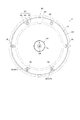
図1は、実施例に係る基板処理装置の全体構成を示した縦断面図であり、図2は、スピンチャックの平面図であり、図3は、気体ノズル及びその周辺を含む構成の縦断面図である。
1 … 基板処理装置
3 … 支持回転機構
5 … 飛散防止カップ
7 … 処理機構
9 … 処理液供給機構
11 … スピンチャック
13 … スピンベース
15 … 支持ピン
17 … 回転軸
19 … 電動モータ
57 … 気体供給管
58 … リンス液供給管
59 … 先端保持部
61 … 開口61
67 … 気体ノズル
69 … ベース部
71 … 整流部材
73 … 脚部
75 … 噴出口
h … 開口高さ
GS1 … 供給配管
GS … 不活性ガス供給源
GS3 … 第1の分岐配管
GS5 … 第2の分岐配管
GS7,GS9 … 制御弁
RS1 … 供給配管
RS3 … 開閉弁
111 … 制御部
Claims (8)
- 基板の下面を処理液で覆った状態で、その上面を処理する基板処理装置において、
鉛直軸周りに回転可能な回転台と、
前記回転台を回転させる回転駆動手段と、
前記回転台に立設され、基板の周縁部と当接して、基板の下面を前記回転台の上面から離間して支持する支持手段と、
前記支持手段で支持された基板の上面に作用して処理を行う処理手段と、
基板の下面に処理液を供給する処理液供給手段と、
前記回転台の中央から前記基板の下面に気体を供給する気体ノズルと、
一端側が前記気体ノズルに連通接続された気体供給管と、
気体を供給する気体供給手段と、
一端側が前記気体供給手段に連通接続され、他端側が前記気体供給管の他端側に連通接続された第1の分岐配管と、
一端側が前記気体供給手段に連通接続され、他端側が前記気体供給管の他端側に連通接続された第2の分岐配管と、
前記第1の分岐配管における気体の流通を第1の流量に制御する第1の制御弁と、
前記第2の分岐配管における気体の流通を、前記第1の流量以上の流量である第2の流量に制御する第2の制御弁と、
前記処理手段で基板の上面を処理する上面処理の際には、前記回転駆動手段を操作して基板を第1の回転数で回転させつつ前記処理液供給手段から処理液を供給させ、前記第1の制御弁を操作して前記気体ノズルから第1の流量で気体を供給させ、前記上面処理が終了した後、前記回転駆動手段の回転数を上昇させて第2の回転数で基板を回転させて基板を乾燥させる乾燥処理の際には、前記第1の制御弁及び前記第2の制御弁を操作して、前記気体ノズルから前記第1の流量より大流量で気体を供給させる制御手段と、
を備え、
前記第1の制御弁及び前記第2の制御弁は、同等または異なる所望の流量に調整可能であることを特徴とする基板処理装置。 - 請求項1に記載の基板処理装置において、
前記第2の流量は、前記第1の流量と同等以上であることを特徴とする基板処理装置。 - 請求項1または2に記載の基板処理装置において、
前記制御手段は、前記第1の制御弁を常時開放させていることを特徴とする基板処理装置。 - 請求項1または2に記載の基板処理装置において、
前記制御手段は、前記第1の制御弁及び前記第2の制御弁を操作する際に、前記第1の制御弁を開放させたまま前記第2の制御弁を開放させることを特徴とする基板処理装置。 - 請求項1から4のいずれかに記載の基板処理装置において、
前記制御手段は、前記第1の回転数から前記第2の回転数へ回転数を上げ始める時点から前記第2の回転数へ到達する時点の間に、前記気体ノズルから第2の流量以上で気体を供給させることを特徴とする基板処理装置。 - 請求項1から5のいずれかに記載の基板処理装置において、
前記気体ノズルは、平面視で、放射状に基板の周縁部に向けて気体を供給することを特徴とする基板処理装置。 - 請求項1から6のいずれかに記載の基板処理装置において、
前記気体ノズルは、気体を供給する開口高さが2mm以上であることを特徴とする基板処理装置。 - 基板の下面を処理液で覆った状態で、その上面を処理する基板処理方法において、
基板の周縁部を当接支持して基板の下面を回転台から離間させた状態で、前記回転台を第1の回転数で回転させ、基板の下面を処理液で覆った状態で、第1の制御弁を操作して前記回転台の中央の気体ノズルから基板の下面に第1の流量で気体を供給しつつ基板の上面を処理する上面処理過程と、
前記回転台を前記第1の回転数よりも高い第2の回転数で回転させ、第1の制御弁及び第2の制御弁を操作して気体ノズルから前記第1の流量より大流量で気体を供給させる乾燥処理過程と、
をその順に実施し、
前記第1の制御弁及び前記第2の制御弁は、同等または異なる所望の流量に調整可能であることを特徴とする基板処理方法。
Priority Applications (5)
| Application Number | Priority Date | Filing Date | Title |
|---|---|---|---|
| JP2017088214A JP6869093B2 (ja) | 2017-04-27 | 2017-04-27 | 基板処理装置及び基板処理方法 |
| TW107113970A TWI719301B (zh) | 2017-04-27 | 2018-04-25 | 基板處理裝置及基板處理方法 |
| US15/962,416 US10910235B2 (en) | 2017-04-27 | 2018-04-25 | Substrate treating apparatus and substrate treating method |
| KR1020180049225A KR102084844B1 (ko) | 2017-04-27 | 2018-04-27 | 기판 처리 장치 및 기판 처리 방법 |
| CN201810390875.5A CN108807223B (zh) | 2017-04-27 | 2018-04-27 | 基板处理装置以及基板处理方法 |
Applications Claiming Priority (1)
| Application Number | Priority Date | Filing Date | Title |
|---|---|---|---|
| JP2017088214A JP6869093B2 (ja) | 2017-04-27 | 2017-04-27 | 基板処理装置及び基板処理方法 |
Publications (2)
| Publication Number | Publication Date |
|---|---|
| JP2018186219A JP2018186219A (ja) | 2018-11-22 |
| JP6869093B2 true JP6869093B2 (ja) | 2021-05-12 |
Family
ID=63917457
Family Applications (1)
| Application Number | Title | Priority Date | Filing Date |
|---|---|---|---|
| JP2017088214A Active JP6869093B2 (ja) | 2017-04-27 | 2017-04-27 | 基板処理装置及び基板処理方法 |
Country Status (5)
| Country | Link |
|---|---|
| US (1) | US10910235B2 (ja) |
| JP (1) | JP6869093B2 (ja) |
| KR (1) | KR102084844B1 (ja) |
| CN (1) | CN108807223B (ja) |
| TW (1) | TWI719301B (ja) |
Families Citing this family (9)
| Publication number | Priority date | Publication date | Assignee | Title |
|---|---|---|---|---|
| JP6887912B2 (ja) * | 2017-08-07 | 2021-06-16 | 東京エレクトロン株式会社 | 基板処理装置、基板処理方法及び記憶媒体 |
| JP7386026B2 (ja) * | 2019-09-20 | 2023-11-24 | 株式会社Screenホールディングス | 基板処理方法および基板処理装置 |
| JP7437899B2 (ja) * | 2019-09-20 | 2024-02-26 | 株式会社Screenホールディングス | 基板処理装置 |
| KR102583342B1 (ko) | 2020-10-22 | 2023-09-26 | 세메스 주식회사 | 기판 처리 장치 |
| JP7558043B2 (ja) | 2020-11-30 | 2024-09-30 | 株式会社Screenホールディングス | 基板処理装置及び基板処理方法 |
| JP7530846B2 (ja) * | 2021-02-19 | 2024-08-08 | 東京エレクトロン株式会社 | 基板処理装置、基板処理方法及びコンピュータ読み取り可能な記録媒体 |
| JP7544625B2 (ja) * | 2021-03-04 | 2024-09-03 | 株式会社Screenホールディングス | 基板処理装置、及び基板処理方法 |
| KR102535766B1 (ko) * | 2021-08-24 | 2023-05-26 | (주)디바이스이엔지 | 백 노즐 어셈블리를 포함하는 기판 처리장치 |
| TWI812123B (zh) * | 2022-03-28 | 2023-08-11 | 辛耘企業股份有限公司 | 晶圓載台 |
Family Cites Families (16)
| Publication number | Priority date | Publication date | Assignee | Title |
|---|---|---|---|---|
| JPH0864490A (ja) | 1993-12-27 | 1996-03-08 | Motoyama Seisakusho:Kk | ガス系の流量制御装置 |
| JP3442604B2 (ja) | 1996-02-15 | 2003-09-02 | 株式会社フジキン | 混合ガスの供給方法及び混合ガス供給装置並びにこれらを備えた半導体製造装置 |
| WO2005015627A1 (en) | 2003-08-07 | 2005-02-17 | Ebara Corporation | Substrate processing apparatus, substrate processing method, and substrate holding apparatus |
| TWI286353B (en) * | 2004-10-12 | 2007-09-01 | Tokyo Electron Ltd | Substrate processing method and substrate processing apparatus |
| JP4662352B2 (ja) | 2005-08-10 | 2011-03-30 | 東京エレクトロン株式会社 | 蒸気乾燥方法及びその装置並びにその記録媒体 |
| JP4415044B2 (ja) * | 2007-12-05 | 2010-02-17 | 大日本スクリーン製造株式会社 | 基板処理方法および基板処理装置 |
| JP5156661B2 (ja) | 2009-02-12 | 2013-03-06 | 東京エレクトロン株式会社 | 液処理装置および液処理方法 |
| JP5472169B2 (ja) * | 2011-03-16 | 2014-04-16 | 東京エレクトロン株式会社 | 液処理装置、液処理方法および記憶媒体 |
| US10133173B2 (en) | 2012-09-27 | 2018-11-20 | SCREEN Holdings Co., Ltd. | Processing fluid supply device, substrate processing device, processing fluid supply method, substrate processing method, processing fluid processing device, and processing fluid processing method |
| JP6231328B2 (ja) * | 2013-08-20 | 2017-11-15 | 株式会社Screenホールディングス | 基板処理方法および基板処理装置 |
| JP6359477B2 (ja) | 2014-08-27 | 2018-07-18 | 東京エレクトロン株式会社 | 基板液処理装置 |
| JP6512554B2 (ja) | 2014-09-29 | 2019-05-15 | 株式会社Screenホールディングス | 基板処理方法および基板処理装置 |
| US10249487B2 (en) | 2015-01-23 | 2019-04-02 | SCREEN Holdings Co., Ltd. | Substrate processing method |
| JP6503194B2 (ja) | 2015-02-16 | 2019-04-17 | 株式会社Screenホールディングス | 基板処理装置 |
| TWI622091B (zh) | 2015-06-18 | 2018-04-21 | 思可林集團股份有限公司 | 基板處理裝置 |
| JP6494480B2 (ja) | 2015-09-25 | 2019-04-03 | 東京エレクトロン株式会社 | 基板液処理装置及び基板液処理装置の基板乾燥方法 |
-
2017
- 2017-04-27 JP JP2017088214A patent/JP6869093B2/ja active Active
-
2018
- 2018-04-25 TW TW107113970A patent/TWI719301B/zh active
- 2018-04-25 US US15/962,416 patent/US10910235B2/en active Active
- 2018-04-27 KR KR1020180049225A patent/KR102084844B1/ko active Active
- 2018-04-27 CN CN201810390875.5A patent/CN108807223B/zh active Active
Also Published As
| Publication number | Publication date |
|---|---|
| US20180315624A1 (en) | 2018-11-01 |
| TW201843730A (zh) | 2018-12-16 |
| KR20180120614A (ko) | 2018-11-06 |
| CN108807223A (zh) | 2018-11-13 |
| TWI719301B (zh) | 2021-02-21 |
| CN108807223B (zh) | 2022-03-01 |
| KR102084844B1 (ko) | 2020-03-04 |
| US10910235B2 (en) | 2021-02-02 |
| JP2018186219A (ja) | 2018-11-22 |
Similar Documents
| Publication | Publication Date | Title |
|---|---|---|
| JP6869093B2 (ja) | 基板処理装置及び基板処理方法 | |
| US9984903B2 (en) | Treatment cup cleaning method, substrate treatment method, and substrate treatment apparatus | |
| KR101280768B1 (ko) | 기판처리장치 및 기판처리방법 | |
| JP4976949B2 (ja) | 基板処理装置 | |
| JP2003001199A (ja) | 基板洗浄装置 | |
| KR20190006052A (ko) | 기판 처리 장치 및 기판 처리 방법 | |
| JP6718714B2 (ja) | 基板処理方法および基板処理装置 | |
| JP2004119717A (ja) | 基板処理方法および基板処理装置 | |
| TW201720542A (zh) | 基板保持旋轉裝置及具備其之基板處理裝置、暨基板處理方法 | |
| CN104517807A (zh) | 基板处理方法以及基板处理装置 | |
| US20200144081A1 (en) | Substrate processing method and substrate processing device | |
| CN103367110B (zh) | 基板处理方法以及基板处理装置 | |
| JP2015019024A (ja) | 基板処理装置 | |
| JP2017041509A (ja) | 基板処理方法および基板処理装置 | |
| JP2003092280A (ja) | 基板乾燥方法 | |
| JP5031654B2 (ja) | 基板処理装置および基板処理方法 | |
| JP6899703B2 (ja) | 基板処理装置および基板処理方法 | |
| JP2018142594A (ja) | 基板処理装置及び基板処理方法 | |
| JP6405259B2 (ja) | 基板処理装置および基板処理方法 | |
| JP2018142593A (ja) | 基板処理装置及び基板処理方法 | |
| JP2006005382A (ja) | 基板処理装置 | |
| JP2009123951A (ja) | 基板処理装置および基板処理方法 | |
| JPH11274135A (ja) | 基板処理装置 | |
| JP2007005391A (ja) | 基板処理装置および基板処理方法 |
Legal Events
| Date | Code | Title | Description |
|---|---|---|---|
| A621 | Written request for application examination |
Free format text: JAPANESE INTERMEDIATE CODE: A621 Effective date: 20191223 |
|
| A977 | Report on retrieval |
Free format text: JAPANESE INTERMEDIATE CODE: A971007 Effective date: 20200813 |
|
| A131 | Notification of reasons for refusal |
Free format text: JAPANESE INTERMEDIATE CODE: A131 Effective date: 20200825 |
|
| A521 | Request for written amendment filed |
Free format text: JAPANESE INTERMEDIATE CODE: A523 Effective date: 20201020 |
|
| TRDD | Decision of grant or rejection written | ||
| A01 | Written decision to grant a patent or to grant a registration (utility model) |
Free format text: JAPANESE INTERMEDIATE CODE: A01 Effective date: 20210330 |
|
| A61 | First payment of annual fees (during grant procedure) |
Free format text: JAPANESE INTERMEDIATE CODE: A61 Effective date: 20210413 |
|
| R150 | Certificate of patent or registration of utility model |
Ref document number: 6869093 Country of ref document: JP Free format text: JAPANESE INTERMEDIATE CODE: R150 |
|
| R250 | Receipt of annual fees |
Free format text: JAPANESE INTERMEDIATE CODE: R250 |
|
| R250 | Receipt of annual fees |
Free format text: JAPANESE INTERMEDIATE CODE: R250 |
|
| R250 | Receipt of annual fees |
Free format text: JAPANESE INTERMEDIATE CODE: R250 |