JP6870164B2 - Display device and manufacturing method of display device - Google Patents
Display device and manufacturing method of display device Download PDFInfo
- Publication number
- JP6870164B2 JP6870164B2 JP2016111987A JP2016111987A JP6870164B2 JP 6870164 B2 JP6870164 B2 JP 6870164B2 JP 2016111987 A JP2016111987 A JP 2016111987A JP 2016111987 A JP2016111987 A JP 2016111987A JP 6870164 B2 JP6870164 B2 JP 6870164B2
- Authority
- JP
- Japan
- Prior art keywords
- housing
- display device
- resin
- display
- front panel
- Prior art date
- Legal status (The legal status is an assumption and is not a legal conclusion. Google has not performed a legal analysis and makes no representation as to the accuracy of the status listed.)
- Active
Links
Images






Classifications
-
- G—PHYSICS
- G02—OPTICS
- G02F—OPTICAL DEVICES OR ARRANGEMENTS FOR THE CONTROL OF LIGHT BY MODIFICATION OF THE OPTICAL PROPERTIES OF THE MEDIA OF THE ELEMENTS INVOLVED THEREIN; NON-LINEAR OPTICS; FREQUENCY-CHANGING OF LIGHT; OPTICAL LOGIC ELEMENTS; OPTICAL ANALOGUE/DIGITAL CONVERTERS
- G02F1/00—Devices or arrangements for the control of the intensity, colour, phase, polarisation or direction of light arriving from an independent light source, e.g. switching, gating or modulating; Non-linear optics
- G02F1/01—Devices or arrangements for the control of the intensity, colour, phase, polarisation or direction of light arriving from an independent light source, e.g. switching, gating or modulating; Non-linear optics for the control of the intensity, phase, polarisation or colour
- G02F1/13—Devices or arrangements for the control of the intensity, colour, phase, polarisation or direction of light arriving from an independent light source, e.g. switching, gating or modulating; Non-linear optics for the control of the intensity, phase, polarisation or colour based on liquid crystals, e.g. single liquid crystal display cells
- G02F1/133—Constructional arrangements; Operation of liquid crystal cells; Circuit arrangements
- G02F1/1333—Constructional arrangements; Manufacturing methods
- G02F1/133308—Support structures for LCD panels, e.g. frames or bezels
-
- G—PHYSICS
- G02—OPTICS
- G02B—OPTICAL ELEMENTS, SYSTEMS OR APPARATUS
- G02B1/00—Optical elements characterised by the material of which they are made; Optical coatings for optical elements
- G02B1/04—Optical elements characterised by the material of which they are made; Optical coatings for optical elements made of organic materials, e.g. plastics
-
- G—PHYSICS
- G02—OPTICS
- G02F—OPTICAL DEVICES OR ARRANGEMENTS FOR THE CONTROL OF LIGHT BY MODIFICATION OF THE OPTICAL PROPERTIES OF THE MEDIA OF THE ELEMENTS INVOLVED THEREIN; NON-LINEAR OPTICS; FREQUENCY-CHANGING OF LIGHT; OPTICAL LOGIC ELEMENTS; OPTICAL ANALOGUE/DIGITAL CONVERTERS
- G02F1/00—Devices or arrangements for the control of the intensity, colour, phase, polarisation or direction of light arriving from an independent light source, e.g. switching, gating or modulating; Non-linear optics
- G02F1/01—Devices or arrangements for the control of the intensity, colour, phase, polarisation or direction of light arriving from an independent light source, e.g. switching, gating or modulating; Non-linear optics for the control of the intensity, phase, polarisation or colour
- G02F1/13—Devices or arrangements for the control of the intensity, colour, phase, polarisation or direction of light arriving from an independent light source, e.g. switching, gating or modulating; Non-linear optics for the control of the intensity, phase, polarisation or colour based on liquid crystals, e.g. single liquid crystal display cells
- G02F1/133—Constructional arrangements; Operation of liquid crystal cells; Circuit arrangements
- G02F1/1333—Constructional arrangements; Manufacturing methods
- G02F1/1343—Electrodes
- G02F1/13439—Electrodes characterised by their electrical, optical, physical properties; materials therefor; method of making
-
- G—PHYSICS
- G02—OPTICS
- G02F—OPTICAL DEVICES OR ARRANGEMENTS FOR THE CONTROL OF LIGHT BY MODIFICATION OF THE OPTICAL PROPERTIES OF THE MEDIA OF THE ELEMENTS INVOLVED THEREIN; NON-LINEAR OPTICS; FREQUENCY-CHANGING OF LIGHT; OPTICAL LOGIC ELEMENTS; OPTICAL ANALOGUE/DIGITAL CONVERTERS
- G02F1/00—Devices or arrangements for the control of the intensity, colour, phase, polarisation or direction of light arriving from an independent light source, e.g. switching, gating or modulating; Non-linear optics
- G02F1/01—Devices or arrangements for the control of the intensity, colour, phase, polarisation or direction of light arriving from an independent light source, e.g. switching, gating or modulating; Non-linear optics for the control of the intensity, phase, polarisation or colour
- G02F1/13—Devices or arrangements for the control of the intensity, colour, phase, polarisation or direction of light arriving from an independent light source, e.g. switching, gating or modulating; Non-linear optics for the control of the intensity, phase, polarisation or colour based on liquid crystals, e.g. single liquid crystal display cells
- G02F1/133—Constructional arrangements; Operation of liquid crystal cells; Circuit arrangements
- G02F1/136—Liquid crystal cells structurally associated with a semi-conducting layer or substrate, e.g. cells forming part of an integrated circuit
-
- H—ELECTRICITY
- H10—SEMICONDUCTOR DEVICES; ELECTRIC SOLID-STATE DEVICES NOT OTHERWISE PROVIDED FOR
- H10K—ORGANIC ELECTRIC SOLID-STATE DEVICES
- H10K50/00—Organic light-emitting devices
- H10K50/80—Constructional details
- H10K50/84—Passivation; Containers; Encapsulations
- H10K50/842—Containers
- H10K50/8426—Peripheral sealing arrangements, e.g. adhesives, sealants
-
- H—ELECTRICITY
- H10—SEMICONDUCTOR DEVICES; ELECTRIC SOLID-STATE DEVICES NOT OTHERWISE PROVIDED FOR
- H10K—ORGANIC ELECTRIC SOLID-STATE DEVICES
- H10K50/00—Organic light-emitting devices
- H10K50/80—Constructional details
- H10K50/84—Passivation; Containers; Encapsulations
- H10K50/844—Encapsulations
-
- H—ELECTRICITY
- H10—SEMICONDUCTOR DEVICES; ELECTRIC SOLID-STATE DEVICES NOT OTHERWISE PROVIDED FOR
- H10K—ORGANIC ELECTRIC SOLID-STATE DEVICES
- H10K50/00—Organic light-emitting devices
- H10K50/80—Constructional details
- H10K50/85—Arrangements for extracting light from the devices
- H10K50/858—Arrangements for extracting light from the devices comprising refractive means, e.g. lenses
-
- H—ELECTRICITY
- H10—SEMICONDUCTOR DEVICES; ELECTRIC SOLID-STATE DEVICES NOT OTHERWISE PROVIDED FOR
- H10K—ORGANIC ELECTRIC SOLID-STATE DEVICES
- H10K59/00—Integrated devices, or assemblies of multiple devices, comprising at least one organic light-emitting element covered by group H10K50/00
- H10K59/80—Constructional details
- H10K59/87—Passivation; Containers; Encapsulations
- H10K59/871—Self-supporting sealing arrangements
- H10K59/8722—Peripheral sealing arrangements, e.g. adhesives, sealants
-
- H—ELECTRICITY
- H10—SEMICONDUCTOR DEVICES; ELECTRIC SOLID-STATE DEVICES NOT OTHERWISE PROVIDED FOR
- H10K—ORGANIC ELECTRIC SOLID-STATE DEVICES
- H10K71/00—Manufacture or treatment specially adapted for the organic devices covered by this subclass
- H10K71/50—Forming devices by joining two substrates together, e.g. lamination techniques
-
- G—PHYSICS
- G02—OPTICS
- G02F—OPTICAL DEVICES OR ARRANGEMENTS FOR THE CONTROL OF LIGHT BY MODIFICATION OF THE OPTICAL PROPERTIES OF THE MEDIA OF THE ELEMENTS INVOLVED THEREIN; NON-LINEAR OPTICS; FREQUENCY-CHANGING OF LIGHT; OPTICAL LOGIC ELEMENTS; OPTICAL ANALOGUE/DIGITAL CONVERTERS
- G02F1/00—Devices or arrangements for the control of the intensity, colour, phase, polarisation or direction of light arriving from an independent light source, e.g. switching, gating or modulating; Non-linear optics
- G02F1/01—Devices or arrangements for the control of the intensity, colour, phase, polarisation or direction of light arriving from an independent light source, e.g. switching, gating or modulating; Non-linear optics for the control of the intensity, phase, polarisation or colour
- G02F1/13—Devices or arrangements for the control of the intensity, colour, phase, polarisation or direction of light arriving from an independent light source, e.g. switching, gating or modulating; Non-linear optics for the control of the intensity, phase, polarisation or colour based on liquid crystals, e.g. single liquid crystal display cells
- G02F1/133—Constructional arrangements; Operation of liquid crystal cells; Circuit arrangements
- G02F1/1333—Constructional arrangements; Manufacturing methods
- G02F1/133308—Support structures for LCD panels, e.g. frames or bezels
- G02F1/133311—Environmental protection, e.g. against dust or humidity
-
- G—PHYSICS
- G02—OPTICS
- G02F—OPTICAL DEVICES OR ARRANGEMENTS FOR THE CONTROL OF LIGHT BY MODIFICATION OF THE OPTICAL PROPERTIES OF THE MEDIA OF THE ELEMENTS INVOLVED THEREIN; NON-LINEAR OPTICS; FREQUENCY-CHANGING OF LIGHT; OPTICAL LOGIC ELEMENTS; OPTICAL ANALOGUE/DIGITAL CONVERTERS
- G02F1/00—Devices or arrangements for the control of the intensity, colour, phase, polarisation or direction of light arriving from an independent light source, e.g. switching, gating or modulating; Non-linear optics
- G02F1/01—Devices or arrangements for the control of the intensity, colour, phase, polarisation or direction of light arriving from an independent light source, e.g. switching, gating or modulating; Non-linear optics for the control of the intensity, phase, polarisation or colour
- G02F1/13—Devices or arrangements for the control of the intensity, colour, phase, polarisation or direction of light arriving from an independent light source, e.g. switching, gating or modulating; Non-linear optics for the control of the intensity, phase, polarisation or colour based on liquid crystals, e.g. single liquid crystal display cells
- G02F1/133—Constructional arrangements; Operation of liquid crystal cells; Circuit arrangements
- G02F1/1333—Constructional arrangements; Manufacturing methods
- G02F1/133308—Support structures for LCD panels, e.g. frames or bezels
- G02F1/13332—Front frames
-
- G—PHYSICS
- G02—OPTICS
- G02F—OPTICAL DEVICES OR ARRANGEMENTS FOR THE CONTROL OF LIGHT BY MODIFICATION OF THE OPTICAL PROPERTIES OF THE MEDIA OF THE ELEMENTS INVOLVED THEREIN; NON-LINEAR OPTICS; FREQUENCY-CHANGING OF LIGHT; OPTICAL LOGIC ELEMENTS; OPTICAL ANALOGUE/DIGITAL CONVERTERS
- G02F1/00—Devices or arrangements for the control of the intensity, colour, phase, polarisation or direction of light arriving from an independent light source, e.g. switching, gating or modulating; Non-linear optics
- G02F1/01—Devices or arrangements for the control of the intensity, colour, phase, polarisation or direction of light arriving from an independent light source, e.g. switching, gating or modulating; Non-linear optics for the control of the intensity, phase, polarisation or colour
- G02F1/13—Devices or arrangements for the control of the intensity, colour, phase, polarisation or direction of light arriving from an independent light source, e.g. switching, gating or modulating; Non-linear optics for the control of the intensity, phase, polarisation or colour based on liquid crystals, e.g. single liquid crystal display cells
- G02F1/133—Constructional arrangements; Operation of liquid crystal cells; Circuit arrangements
- G02F1/1333—Constructional arrangements; Manufacturing methods
- G02F1/133308—Support structures for LCD panels, e.g. frames or bezels
- G02F1/133325—Assembling processes
-
- G—PHYSICS
- G02—OPTICS
- G02F—OPTICAL DEVICES OR ARRANGEMENTS FOR THE CONTROL OF LIGHT BY MODIFICATION OF THE OPTICAL PROPERTIES OF THE MEDIA OF THE ELEMENTS INVOLVED THEREIN; NON-LINEAR OPTICS; FREQUENCY-CHANGING OF LIGHT; OPTICAL LOGIC ELEMENTS; OPTICAL ANALOGUE/DIGITAL CONVERTERS
- G02F1/00—Devices or arrangements for the control of the intensity, colour, phase, polarisation or direction of light arriving from an independent light source, e.g. switching, gating or modulating; Non-linear optics
- G02F1/01—Devices or arrangements for the control of the intensity, colour, phase, polarisation or direction of light arriving from an independent light source, e.g. switching, gating or modulating; Non-linear optics for the control of the intensity, phase, polarisation or colour
- G02F1/13—Devices or arrangements for the control of the intensity, colour, phase, polarisation or direction of light arriving from an independent light source, e.g. switching, gating or modulating; Non-linear optics for the control of the intensity, phase, polarisation or colour based on liquid crystals, e.g. single liquid crystal display cells
- G02F1/133—Constructional arrangements; Operation of liquid crystal cells; Circuit arrangements
- G02F1/1333—Constructional arrangements; Manufacturing methods
- G02F1/133308—Support structures for LCD panels, e.g. frames or bezels
- G02F1/133331—Cover glasses
-
- G—PHYSICS
- G02—OPTICS
- G02F—OPTICAL DEVICES OR ARRANGEMENTS FOR THE CONTROL OF LIGHT BY MODIFICATION OF THE OPTICAL PROPERTIES OF THE MEDIA OF THE ELEMENTS INVOLVED THEREIN; NON-LINEAR OPTICS; FREQUENCY-CHANGING OF LIGHT; OPTICAL LOGIC ELEMENTS; OPTICAL ANALOGUE/DIGITAL CONVERTERS
- G02F1/00—Devices or arrangements for the control of the intensity, colour, phase, polarisation or direction of light arriving from an independent light source, e.g. switching, gating or modulating; Non-linear optics
- G02F1/01—Devices or arrangements for the control of the intensity, colour, phase, polarisation or direction of light arriving from an independent light source, e.g. switching, gating or modulating; Non-linear optics for the control of the intensity, phase, polarisation or colour
- G02F1/13—Devices or arrangements for the control of the intensity, colour, phase, polarisation or direction of light arriving from an independent light source, e.g. switching, gating or modulating; Non-linear optics for the control of the intensity, phase, polarisation or colour based on liquid crystals, e.g. single liquid crystal display cells
- G02F1/133—Constructional arrangements; Operation of liquid crystal cells; Circuit arrangements
- G02F1/1333—Constructional arrangements; Manufacturing methods
- G02F1/13338—Input devices, e.g. touch panels
-
- G—PHYSICS
- G02—OPTICS
- G02F—OPTICAL DEVICES OR ARRANGEMENTS FOR THE CONTROL OF LIGHT BY MODIFICATION OF THE OPTICAL PROPERTIES OF THE MEDIA OF THE ELEMENTS INVOLVED THEREIN; NON-LINEAR OPTICS; FREQUENCY-CHANGING OF LIGHT; OPTICAL LOGIC ELEMENTS; OPTICAL ANALOGUE/DIGITAL CONVERTERS
- G02F2202/00—Materials and properties
- G02F2202/28—Adhesive materials or arrangements
Landscapes
- Physics & Mathematics (AREA)
- Nonlinear Science (AREA)
- Optics & Photonics (AREA)
- General Physics & Mathematics (AREA)
- Mathematical Physics (AREA)
- Chemical & Material Sciences (AREA)
- Crystallography & Structural Chemistry (AREA)
- Engineering & Computer Science (AREA)
- Manufacturing & Machinery (AREA)
- Microelectronics & Electronic Packaging (AREA)
- Devices For Indicating Variable Information By Combining Individual Elements (AREA)
- Liquid Crystal (AREA)
Description
本発明は、表示装置および表示装置の製造方法に関する。 The present invention relates to a display device and a method for manufacturing the display device.
近年、表示パネルを搭載した表示モジュールの表面に、タッチパネルまたは強化ガラス等の前面パネルを搭載した表示装置が増えている。タッチパネルは、表示装置の入力デバイスとして用いられる。強化ガラスは、表示面の保護用に用いられる。強化ガラスは、表示装置のデザイン性向上の観点から加飾印刷される場合がある。 In recent years, an increasing number of display devices have a front panel such as a touch panel or tempered glass mounted on the surface of a display module equipped with a display panel. The touch panel is used as an input device of the display device. Tempered glass is used to protect the display surface. The tempered glass may be decoratively printed from the viewpoint of improving the design of the display device.
表示モジュールに前面パネルを配置する方法として、表示モジュール内の表示パネルと前面パネルとを、接着剤などを用いて周辺部で貼り合せる方法がある。表示パネルと前面パネルとの間には、空気層が介在する。この貼合方法は、便宜上エアギャップボンディング(Air Gap Bonding)と呼ばれる。しかし、前面パネルおよび表示パネルの屈折率と空気層の屈折率とが大きく異なるため、空気層の両側の界面で光の反射が生じてしまう。そのためエアギャップボンディングには、表示画像の視認性が著しく低下するという問題がある。この視認性が著しく低下する現象は、特に外光環境下で顕著に表れる。 As a method of arranging the front panel on the display module, there is a method of sticking the display panel and the front panel in the display module at the peripheral portion by using an adhesive or the like. An air layer is interposed between the display panel and the front panel. This bonding method is called Air Gap Bonding for convenience. However, since the refractive index of the front panel and the display panel and the refractive index of the air layer are significantly different, light is reflected at the interfaces on both sides of the air layer. Therefore, the air gap bonding has a problem that the visibility of the displayed image is remarkably lowered. This phenomenon of significantly reduced visibility is particularly noticeable in an external light environment.
視認性の低下を軽減するため、空気層部分に前面パネルと近しい屈折率を有する光学弾性樹脂(以下OCR(Optical Clear Resin)と記載する)を充填して、表示パネルと前面パネルとを貼り合せる方法が用いられている。界面反射を抑制し、画像表示の視認性を向上させることが可能である。この技術はオプティカルボンディング(Optical-Bonding)、あるいはダイレクトボンディング(Direct-Bonding)と呼ばれている。前面パネルの耐衝撃性向上および破損時の飛散防止といった機械的な効果もあることから広く採用されるようになってきている。 In order to reduce the decrease in visibility, the air layer portion is filled with an optical elastic resin (hereinafter referred to as OCR (Optical Clear Resin)) having a refractive index close to that of the front panel, and the display panel and the front panel are bonded together. The method is used. It is possible to suppress interfacial reflection and improve the visibility of image display. This technique is called Optical-Bonding or Direct-Bonding. It has been widely adopted because it has mechanical effects such as improving the impact resistance of the front panel and preventing scattering when it is damaged.
しかしながら、表示パネルを構成している上下基板は、構造上外部ストレスに弱い。上下基板に加わる局所的なストレスは、ムラや変色などの表示不良を誘発する。上記表示装置では、前面パネルを通して表示モジュールにストレスが加わるため、新たな製品設計や製造プロセス設計が求められている。 However, the upper and lower substrates constituting the display panel are structurally vulnerable to external stress. Local stress applied to the upper and lower substrates induces display defects such as unevenness and discoloration. In the above display device, stress is applied to the display module through the front panel, so that new product design and manufacturing process design are required.
前述のようなOCRを介して前面パネルが取り付けられた表示装置の構造並びに製造プロセスは、大きく二分される。一つは、表示パネルを構成している上下基板の表面に前面パネルを貼り合せ、その後にケース部とハウジングとの間に収容する、ハウジングアウト方式である(特許文献1)。もう一つは上下基板を搭載した表示モジュールの表面に前面パネルを貼り合せる、ハウジングイン方式である(特許文献2)。 The structure and manufacturing process of the display device to which the front panel is attached via the OCR as described above is roughly divided into two. One is a housing-out method in which a front panel is attached to the surface of the upper and lower substrates constituting the display panel, and then the front panel is accommodated between the case portion and the housing (Patent Document 1). The other is a housing-in method in which a front panel is attached to the surface of a display module on which upper and lower boards are mounted (Patent Document 2).
前者のハウジングアウト方式は、前面パネル搭載を前提とした専用設計が必要になるため、部材共用が困難で製品開発費用が膨らむ。しかしながら、設計的な対策を製品に盛り込み易い。したがって、開発コストを十分に回収できる多ロット生産の製品向けのプロセスであると言える。ハウジングアウト方式の場合には、前面パネルの表面と上下基板の裏面とを両側から平面で保持して均一に加圧することができる。仮にOCRがOCRをシールする樹脂部材を越えて漏れ出した場合でも、OCRにUV(UltraViolet)硬化樹脂を用いれば、漏れ出したOCRを後から硬化させることが可能であるため、比較的製造が容易である。 The former housing-out method requires a special design that is premised on mounting on the front panel, which makes it difficult to share parts and increases product development costs. However, it is easy to incorporate design measures into the product. Therefore, it can be said that it is a process for multi-lot production products that can sufficiently recover the development cost. In the case of the housing-out method, the front surface of the front panel and the back surface of the upper and lower substrates can be held flat from both sides and uniformly pressurized. Even if OCR leaks beyond the resin member that seals OCR, if UV (UltraViolet) curable resin is used for OCR, the leaked OCR can be cured later, so it is relatively easy to manufacture. It's easy.
後者のハウジングイン方式は、前者とは逆に、部材共用や初期費用回収は容易だが、設計的な対策を盛り込み難い。そのため、課題解決は製造プロセス側で求められることが多くなる。したがって、開発コストを最小限に抑えたい小ロット向けのプロセスと言える。上下基板の裏面にはケース部の外周部以外に支えが無いため、平面で均一に加圧することができない。仮にOCRが樹脂部材を越えて漏れ出した場合、漏れ出したOCRをUV硬化させることができない。そのため、OCRが表示モジュールの内部を汚染してしまう。これらの課題の解決方法が求められている。 Contrary to the former, the latter housing-in method makes it easy to share materials and recover initial costs, but it is difficult to incorporate design measures. Therefore, problem solving is often required on the manufacturing process side. Therefore, it can be said that it is a process for small lots that wants to minimize the development cost. Since there is no support on the back surface of the upper and lower substrates other than the outer peripheral portion of the case portion, it is not possible to uniformly pressurize on a flat surface. If the OCR leaks beyond the resin member, the leaked OCR cannot be UV-cured. Therefore, OCR contaminates the inside of the display module. There is a need for solutions to these issues.
一方、視認性については、オプティカルボンディングより劣るエアギャップボンディングには、OCRを使用せず比較的低コストで製造できるという利点がある。エアギャップボンディングの場合でも、表示モジュールと前面パネルとの間の空隙への異物侵入による表示品質の低下が課題となっている。そのため、単純に表示モジュールに前面パネルを貼り合せるだけではなく、オプティカルボンディングと同様に、表示品質の向上が求められている。 On the other hand, in terms of visibility, air gap bonding, which is inferior to Opticarbonding, has an advantage that it can be manufactured at a relatively low cost without using OCR. Even in the case of air gap bonding, there is a problem of deterioration of display quality due to foreign matter entering the gap between the display module and the front panel. Therefore, it is required not only to simply attach the front panel to the display module but also to improve the display quality as in the case of Opticarbond.
本発明の目的は、表示パネルと前面パネルとをハウジングイン方式で貼り合せる表示装置において、表示装置の表示品質を向上させると同時に、製造を容易にして製造歩留を向上させることが可能な表示装置を提供することである。 An object of the present invention is a display device in which a display panel and a front panel are bonded to each other by a housing-in method, and a display capable of improving the display quality of the display device and at the same time facilitating manufacturing and improving the manufacturing yield. To provide a device.
本願発明の表示装置は、貼合された上下基板と、前記上下基板を収納するケース部と、表示部が開口しているハウジングとを含む表示モジュールと、前記ハウジングの開口の全周に沿って前記上下基板上に設けられており、形成開始端と形成終了端とが前記開口の周方向に重なって他の部分に比べて膨らんだ接合部を有する樹脂部材と、前記樹脂部材を挟んで前記表示モジュールと対向する前面パネルとを有し、前記ハウジングは、前記上下基板と前記前面パネルとの間に挟まれるように設けられ、さらに前記ハウジングの開口端部の稜線の前記接合部に対応する箇所に加工面が設けられており、前記樹脂部材は、前記ハウジングの開口端部の全周に接触し、なおかつ前記ハウジングの上面に端掛けされるように設けられている。 The display device of the present invention includes a display module including a bonded upper and lower substrates, a case portion for accommodating the upper and lower substrates, and a housing in which the display portion is open, and along the entire circumference of the opening of the housing. wherein provided on the upper and lower substrates, and the resin member and the forming start end and the forming completion end has a joint portion bulged as compared with other portions I circumferentially Do heavy said opening, across said resin member The housing has a front panel facing the display module, and the housing is provided so as to be sandwiched between the upper and lower substrates and the front panel, and further, at the joint portion of the ridgeline of the opening end portion of the housing. A processed surface is provided at a corresponding portion, and the resin member is provided so as to be in contact with the entire circumference of the open end portion of the housing and to be end-mounted on the upper surface of the housing.
表示装置の表示品質および製造歩留を向上することができる。 The display quality and manufacturing yield of the display device can be improved.
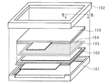
図1は、ハウジングイン方式で製造された表示装置の構成を示す模式分解斜視図である。貼り合された上下基板100、それを支持および収納するケース部101および表示部分が開口されたハウジング102を含むユニットを表示モジュール103と呼ぶ。上下基板100は、例えばカラーフィルタ(CF(Color Filter))基板と薄膜トランジスタ(TFT(Thin Film Transistor))基板からなる液晶表示パネルである。ケース部101は、例えば、バックライトユニットである。ハウジング102は、例えば、金属ベゼルである。
FIG. 1 is a schematic exploded perspective view showing the configuration of a display device manufactured by the housing-in method. A unit including the bonded upper and
表示モジュール103の表示部に、透明な樹脂であるOCR104を介して前面パネル106を全面的に貼り合せた表示装置がある(図1参照)。前面パネル106は、例えば、投影型静電容量式タッチパネルPCAP(Projected Capacitive Touch panel)または強化ガラスである。
On the display unit of the
このような表示装置を製造するに当たって、硬化する前のOCR104が表示モジュール103内部に漏れ出さないよう、ハウジング102と上下基板100との隙間に樹脂製のシール材をあらかじめ形成しておく手法がある。便宜上、このシール材を設けることをダム形成、使用する樹脂をダム材、形成されたシール部分を樹脂ダム(樹脂部材)105と呼ぶ。
In manufacturing such a display device, there is a method of forming a resin sealing material in advance in the gap between the
ハウジングアウト方式の基本的な製造プロセスは、特許文献1に公開されている。ハウジングイン方式の基本的な製造プロセスは、特許文献2に公開されている。どちらの製造プロセス(および製品構造)を選択するかは、製品の仕様、開発コストおよび事業方針等による。本願発明においては、ハウジングイン方式での課題解決を目指している。 The basic manufacturing process of the housing-out method is published in Patent Document 1. The basic manufacturing process of the housing-in method is published in Patent Document 2. Which manufacturing process (and product structure) to choose depends on the product specifications, development costs, business policy, etc. In the present invention, it is aimed to solve the problem by the housing-in method.
比較例であるハウジングアウト方式の製造プロセスの概略を図2に示す。ハウジングイン方式の製造プロセスの概略を図3に示す。ハウジングアウト方式で製造された表示装置の構成を図4に示す。ハウジングイン方式で製造された表示装置の構成を先にあげた図1に示す。 FIG. 2 shows an outline of the manufacturing process of the housing-out method, which is a comparative example. The outline of the housing-in method manufacturing process is shown in FIG. FIG. 4 shows the configuration of the display device manufactured by the housing-out method. The configuration of the display device manufactured by the housing-in method is shown in FIG.
図2を使用して、ハウジングアウト方式の製造プロセスの概略を説明する。図2Aに示すように、ワークである上下基板100を水平な状態に配置して、以後の工程の準備を行う。図2Bに示すように、ディスペンス装置300を用いて上下基板100の縁に沿って一筆書きによりダム材を塗布する。この際、塗布を開始する形成開始端502(図11参照)と、塗布を終了する形成終了端503(図11参照)とが重なる樹脂ダム接合部504(図11参照)も形成される。なお、ダム材の塗布を2回以上に分けて行っても良い。このようにする場合には、樹脂ダム接合部504も複数形成される。紫外線ランプ301を用いてUV照射を行い、ダム材を硬化させて樹脂ダム105を形成する。
FIG. 2 will be used to outline the housing-out manufacturing process. As shown in FIG. 2A, the upper and
図2Cに示すように、樹脂ダム105の内側にOCR104を塗布する。OCR104は、複数のノズルを有するディスペンス装置300を用いて、一様な厚さに塗布することが望ましい。図2Dに示すように、前面パネル106をかぶせることにより、上下基板100と前面パネル106との間にOCR104を挟む。この際、上下基板100の下面を保持しながら、前面パネル106の上面に荷重を加える(図9B参照)。
As shown in FIG. 2C, OCR104 is applied to the inside of the
図2Eに示すように、紫外線ランプ301を用いて弱いUV照射を行い、OCR104を仮硬化させる。図2Fに示すように、強力紫外線ランプ302を用いて強いUV照射を行い、OCR104を完全硬化させる。その後、前面パネル106が固定された上下基板100を、ケース部101とハウジング102との間に組み込む。
As shown in FIG. 2E, weak UV irradiation is performed using the
図3を使用して、ハウジングイン方式の製造プロセスの概略を説明する。ハウジングアウト方式と同様の部分については、説明を省略する。図3Aに示すように、ワークである表示モジュール103を水平な状態に配置して、以後の工程の準備を行う。図3Bに示すように、ディスペンス装置300を用いてハウジング102の開口端部に沿って一筆書きによりダム材を塗布する。紫外線ランプ301を用いてUV照射を行い、ダム材を硬化させて樹脂ダム105を形成する。
FIG. 3 will be used to outline the housing-in manufacturing process. The description of the same part as the housing-out method will be omitted. As shown in FIG. 3A, the
図3Cに示すように、樹脂ダム105の内側にOCR104を塗布する。図3Dに示すように、前面パネル106をかぶせることにより、表示モジュール103と前面パネル106との間にOCR104を挟む。この際、ケース部101の下面を保持しながら、前面パネル106の上面に荷重を加える(図9A参照)。
As shown in FIG. 3C, OCR104 is applied to the inside of the
図3Eに示すように、紫外線ランプ301を用いて弱いUV照射を行い、OCR104を仮硬化させる。図3Fに示すように、強力紫外線ランプ302を用いて強いUV照射を行い、OCR104を完全硬化させる。以上により、表示モジュール103と前面パネル106とが固定される。
As shown in FIG. 3E, weak UV irradiation is performed using the
図5は、樹脂ダム105の形状がハウジング102の開口端部に沿って変化する場合の例を示す模式拡大斜視図である。図5は、ハウジングイン方式の場合を示す。ディスペンス装置300からのダム材の吐出量の変動等により、ハウジング102の開口端部に沿って、図5に示すように樹脂ダム105の太さ、形状および位置等が変動する場合がある。なお、ディスペンス装置300は、このような変動をできるだけ抑制するように、設定される。
FIG. 5 is a schematic enlarged perspective view showing an example in which the shape of the
以下の説明において、図5中に示す切断線で切断した模式断面図を使用する場合がある。模式断面図の図番と、図5中の切断位置との関係は、切断線の両端に示す符号により示す。 In the following description, a schematic cross-sectional view cut along the cutting line shown in FIG. 5 may be used. The relationship between the drawing number of the schematic cross-sectional view and the cutting position in FIG. 5 is indicated by the reference numerals shown at both ends of the cutting line.
ハウジングイン方式とハウジングアウト方式のそれぞれの表示装置の断面構造(図1のVI−VI断面と、図4のVI−VI断面)の比較を図6に示す。ハウジングイン方式(図3参照)が、ハウジングアウト方式(図2参照)と異なる点は、以下の通りである。準備するワークが、上下基板100から表示モジュール103であること。樹脂ダム105を配置する場所が、上下基板100の外周ではなくハウジング102の開口端部であること。前面パネル106の接着後に組込作業が不要なこと。
FIG. 6 shows a comparison of the cross-sectional structures (VI-VI cross-section of FIG. 1 and VI-VI cross-section of FIG. 4) of each of the housing-in type and housing-out type display devices. The difference between the housing-in method (see FIG. 3) and the housing-out method (see FIG. 2) is as follows. The workpiece to be prepared is the upper and
ハウジングアウト方式とハウジングイン方式とでは、製造順序が異なるため、部材配置と形状に違いが生じる。図6に示す通り、ハウジングアウト方式(図6B参照)では、貼り合される上下基板100と前面パネル106の間には、接着剤であるOCR104とOCR104の漏れを抑制する樹脂ダム105しか存在しない。ハウジングイン方式(図6A参照)では、上下基板100と前面パネル106との間にハウジング102も存在する。したがって、ハウジングイン方式の場合には、貼り合せ時の上下基板100の保持構造と、OCR104およびダム105材へのUV照射手順とに制限が加わる。
Since the manufacturing order is different between the housing-out method and the housing-in method, the member arrangement and the shape are different. As shown in FIG. 6, in the housing-out method (see FIG. 6B), there is only a
図7から図11は、課題を説明する図である。図7において、「OK」はOCR104または樹脂ダム105にUV照射を行えることを示している。図7において、「NG」は、ハウジング102等の非透光性の部材に遮られて、OCR104または樹脂ダム105にUV照射を行えないことを示している。ハウジングアウト方式(図7B参照)の場合は、UV照射方向に制限は有るものの、UV照射が不可能な領域は存在しない。したがって樹脂ダム105を越えてOCR104が漏れ出すということについて注意する必要はない。
7 to 11 are diagrams for explaining the problem. In FIG. 7, "OK" indicates that the
一方、ハウジングイン方式(図7A参照)の場合は、上下基板100とハウジング102に挟まれた空間に、UV照射が不可能な領域(UV照射不能域)501が存在する。ハウジングイン方式の場合には、UV照射不能域501を解消することはできない。したがって、樹脂が漏れ出さないように対策を施すか、あらかじめUV照射不能域501を何らかの方法で埋めておくかの対策が必要である。しかし、ハウジングイン方式において、上下基板100とハウジング102の間に物を挟むことは、表示異常を誘発する恐れがある上、材料コスト増の原因にもなる。そのため、UV照射不能域501に樹脂ダム105材およびOCR104等の樹脂を漏れ出させないための対策を講じる必要がある。
On the other hand, in the case of the housing-in method (see FIG. 7A), a region (UV irradiation impossible region) 501 where UV irradiation is impossible exists in the space sandwiched between the upper and
ハウジングイン方式でのダム形成位置には、大まかに二通りがある。一つは、ハウジング102に接触している(図8A参照)場合、もう一つは、非接触(図8B参照)の場合である。非接触の場合には、もしOCR104が樹脂ダム105を越えて漏れ出した場合には、OCR104がUV照射不能域501へ浸入する。UV照射不能域501へ浸入したOCR104をUV硬化させることはできない。硬化させることができなかったOCR104は、後々表示面内へ染み出し表示異常を誘発するおそれがある。
There are roughly two types of dam formation positions in the housing-in method. One is in contact with the housing 102 (see FIG. 8A) and the other is in non-contact (see FIG. 8B). In the case of non-contact, if the
ハウジング102に樹脂ダム105が接触していれば(図8A参照)、OCR104が樹脂ダム105を越えて漏れ出した場合でも、OCR104をUV硬化させることができる。よってハウジングイン方式での樹脂ダム105は、ハウジング102に接触していることが望ましい。このとき、樹脂ダム105は、OCR104のはみ出しを抑制する役割と、はみ出したOCR104がUV照射不能域501へ浸入することを防止する役割との二つの役割を有する。
If the
ハウジングイン方式でのワークである上下基板100はケース部101の周囲辺でのみ保持されている。そのため、前面パネル106に荷重が加わった場合には、上下基板100の中央部が沈み込んでたわむ(図9A参照)。このようなたわみ現象は、ハウジングアウト方式(図9B参照)では発生しない。
The upper and
ハウジング102は0.4〜1.0ミリメートル程度の厚みである。したがって、樹脂ダム105とハウジング102の開口端部との間の接着面積は小さい。そのため、図9Aを使用して説明した上下基板100がたわむ現象により、荷重に耐えきれずに、樹脂ダム105がハウジング102の開口端部から乖離する場合がある。乖離が生じた場合には、硬化前のOCR104が、樹脂ダム105を越えてUV照射不能域501に漏れ出してしまう(図10参照)。
The
このような現象に対する対策として、ハウジング102と乖離し難いダム材を選択する方法も考えられる。しかし、下記の理由により、その方法の採用は困難である。まず、前面パネル106付きの表示装置としての用途を考えた場合には、ダム材には以下のような様々な特性が要求される。表示装置として視認の邪魔にならない透明性を有すること。OCR104との相性が良いこと。UV硬化後に、表示異常(押圧ムラや波紋状のムラ)を起こさない程度の柔らかさ(硬度)を有すること。OCR104のはみ出しを抑制する強靱性を有すること。硬化前のディスペンス精度および作業性に影響する粘度が、適正な値であること。ハウジング102から乖離し難い接着性を備えること。ダム材およびOCR104の物性については、特許文献3にも開示されている。しかし、特許文献3においては、ダム材とハウジング102との接着性について考慮されていない。それ故に、構造や形状での工夫が必要になる。
As a countermeasure against such a phenomenon, a method of selecting a dam material that does not easily deviate from the
ダム材の形状の工夫として、特許文献2には、樹脂ダム105をハウジング102の開口端を覆うように形成する技術が開示されている(実施例3)。しかしながら、OCR104として上下基板(表示パネル)100側に第1接着剤、前面パネル(透光性基板)106側に第2接着剤を形成して、貼り合せを行うため、製造工程が複雑になる。
As a device for the shape of the dam material, Patent Document 2 discloses a technique for forming the
さらに、未硬化のダム材がUV照射不能域501に流れ込まないようにするため、ダム材を素早く硬化させる必要がある。これにより、ダム材の形成開始端502と形成終了端503との接合部である樹脂ダム接合部504が膨らむという問題を生じる(図11参照)。表示パネルのように貼り合わされた上下基板100をワークとする場合には、この樹脂ダム接合部504の膨らみ508が製品として許容される範囲は狭い。局所的な膨らみ508がある場合には、その場所を基点として、表示異常(押圧ムラや波紋状のムラ)が発生するおそれがあるからである。したがって、ディスペンス装置300を用いて樹脂ダム105を塗布する際に、適正な範囲に条件を制御することが困難な場合がある。
Further, in order to prevent the uncured dam material from flowing into the UV irradiation
膨らみ508の適合性について、図12を用いて説明する。樹脂ダム105の形成開始端502と終了端503との接合部である樹脂ダム接合部504の膨らみ508が、周囲の樹脂ダムの高さ507より低いこと、および樹脂ダム接合部504の凹みがUV照射不能域501へ通じていないことの両方が必要である。
The suitability of the
図12Aから図12Eは、膨らみ508の形状の異なる5種類の例を示す。図12の各図の上側は、図11に示す斜視図を図中上側から見た上面図である。図12の各図の下側は、図11に示す斜視図を図中右側から見た側面図である。図12Aおよび図12Bは、膨らみ508が周囲より高いため、不適合である。図12Cおよび図12Dは、膨らみ508が周囲より低く、凹みが照射不能域501へ通じていないため、適合である。図12Eは凹みがUV照射不能域501へ通じているため不適合である。
12A to 12E show five types of
前述の通り、ハウジング102は、厚みが0.4〜1.0ミリメートル程度である。そのため、ディスペンス装置300の形成条件(ノズル幅、塗付位置、吐出開始および終了のタイミング、吐出圧力、吐出速度、サックバック圧力など)の調整を行い、図12Cまたは図12Dの形状を安定的に作製することは困難である。
As described above, the
まず最初に、本願発明に係る表示装置の全体の構成について説明する。表示モジュール103は、貼合された上下基板100、上下基板100を収納するケース部101および表示部が開口しているハウジング102を含む。表示装置は、表示モジュール103と、上下基板100の表面にOCR104およびOCR104の漏えいを抑制する樹脂部材105を介して貼り付けられた前面パネル106を有する(図1参照)。
First, the entire configuration of the display device according to the present invention will be described. The
表示モジュール103のハウジング102は、上下基板100と前面パネル106の間に挟まれる位置に配置されている。ハウジング102の開口端部には、樹脂部材105が接触している。樹脂部材105は、単純にハウジング102に接触しているだけでなく、ハウジング102と樹脂部材105との乖離防止のため、ハウジング102の上面(前面パネル106側の面)に端掛けされるように設けられている(図6A参照)。
The
このような構造にすることにより、OCR104のはみ出しを抑制することが可能である。さらにOCR104がはみ出した場合であっても、またはみ出したOCR104が表示モジュール103の内部へ浸入することを防止することができる。
With such a structure, it is possible to suppress the protrusion of the
樹脂部材105の形状および高さの変動を吸収するために、樹脂部材105が端掛けされているハウジング102の開口端部に、部分的にコーナー処理が施されている。具体的には、樹脂部材105の接合部である樹脂ダム接合部504に対応する位置に、部分的なコーナー処理(斜面、L字面、凹曲面、凸曲面等の加工面500)を施す。コーナー処理により樹脂部材105の膨らみ508を抑えて、表示異常の発生を防止する。
In order to absorb fluctuations in the shape and height of the
製造設備および製造条件の調整により、樹脂ダム接合部504の膨らみ508を解消できない場合がある。例をあげると、選択したダム材が硬く、樹脂ダム接合部504の膨らみ508の影響をダイレクトにワークへ伝えてしまう場合、または樹脂ダム接合部504に残る少しの膨らみ508によっても、過敏に表示異常が起こるワークである場合である。このような場合であっても、樹脂ダム接合部504に位置するハウジング102の開口端部の一部分にコーナー処理を施して加工面500(図14参照)を設けておくことで、表示異常を軽減できる。加工面500は、具体的には斜面、L字面、凹曲面、凸曲面の少なくともいずれかである。実現可能なコーナー処理の形状、深さ、面積は、ハウジング102の厚みおよび材質に依存する。
The
コーナー処理を施すことにより、加工面500の深さ分だけ樹脂ダム接合部504の膨らみ508を低くすることができる。そのため、表示異常を発生させず、ハウジング102から乖離しない樹脂ダム105の形成が容易となる。このため、表示装置の表示品質および製造歩留を向上できる。またダム材および使用する設備の選択肢を広げることも可能になる。
By performing the corner treatment, the
ハウジング102は、前面パネル106との貼り合せが不要な表示モジュール製品との共用が可能であるので、開発コストを抑制できる。前面パネル106を後からハウジングイン方式で貼り合せることを見越して、設計および開発を進めておくことにより、追加開発費用も不要となる。
Since the
以下では、タッチパネル付き液晶表示装置を例に説明を行うが、これに限定されるものでは無い。押圧によって表示異常を起こす上下基板100が、ハウジング102とケース部101との間に組み込まれた表示モジュール103の表示面に、前面パネル106を貼り合せる表示装置すべてに同様の効果が期待できる。上下基板100は、例えばプラズパネル、有機ELパネルおよび電子ペーパーパネル等である。前面パネル106は、例えばタッチパネルまたは補強ガラス等である。
In the following, a liquid crystal display device with a touch panel will be described as an example, but the description is not limited to this. The same effect can be expected for all display devices in which the
構造上、貼り合わされた上下基板100と前面パネル106との間にハウジング102が挟まれており、ダム材がハウジング102の上面端部(前面パネル106側の表面端部)に端掛けされていることが必要である。ハウジング102の材質には特に制約は無いが、一般的に金属板金または樹脂成型が用いられる。以下の説明では金属ベゼルを例に取り上げる。
Structurally, the
図13は、ハウジング102の基本断面形状を示す図である。上下基板100と接触する可能性のあるハウジング102の裏面は、表示異常(押圧ムラや波紋状のムラ)を誘発しない程度に平滑面であることが望ましい。ハウジング102の裏面は、表示異常を誘発しなければ、どのような状態や形状でも構わない。上下基板100の厚みを調整するための形状(図13参照)や電気的な導通を目的とした金属片など、付属品の有無は特に問わない。
FIG. 13 is a diagram showing a basic cross-sectional shape of the
以下の説明は余計な形状や付属物の無い平滑面形状(図13A参照)を使用して行う。ハウジング102の開口端部の前面パネル106側の表面基準線505と側面基準線506とが交わる稜線の部分に、以下に説明するコーナー処理を施す。
The following description will be given using a smooth surface shape (see FIG. 13A) with no extra shape or accessories. The corner treatment described below is applied to the portion of the ridge line where the
図14は、図13との組み合わせで展開できるハウジング102の開口端部のコーナー処理の加工面500の形状を示す模式断面図である。図14Aは斜面、図14BはL字面、図14Cは凹曲面、図14Dは凸曲面の加工面500を示す。コーナー処理された後のハウジング102の開口端部が、表面基準線505および側面基準線506からはみ出さずに内側に後退しており、両基準線の交点o(コーナー処理を実施しない場合のハウジング102の稜線)に達していなければ、任意のコーナー処理形状を採用することができる。コーナー処理形状は、それぞれの複合形状であっても良い。複合形状の具体例については後述する。
FIG. 14 is a schematic cross-sectional view showing the shape of the processed
効果が期待できる順に並べると、図14B>図14C>図14A>図14Dである。寸法的にはa≧0.5ミリメートル且つb≧0.1ミリメートルが望ましい。ハウジング102の材質および加工方法によって、製作可能なコーナー処理部の形状は異なる。以下の説明は図14Aおよび図14Bに示す形状で行う。
Arranged in the order in which the effects can be expected, FIG. 14B> FIG. 14C> FIG. 14A> FIG. 14D. Dimensionally, a ≧ 0.5 mm and b ≧ 0.1 mm are desirable. The shape of the corner processing portion that can be manufactured differs depending on the material and processing method of the
図15は、ハウジング102の開口端部のコーナー処理による加工面500の配置位置と幅(ハウジング102の開口端部に沿う長さ)とを示す部分断面図である。コーナー処理が施される位置は、図15に示すように、樹脂ダム接合部504に対応する位置である。コーナー処理が施される部分の幅は、少なくとも樹脂ダム接合部504の樹脂が膨らんでいる部分を含む長さとする。
FIG. 15 is a partial cross-sectional view showing the arrangement position and width (length along the open end of the housing 102) of the machined
図16は上記の樹脂ダム接合部504に対応する位置に加え、さらにハウジング102の開口端部全周にも加工面500が設けられる場合を示している。図16Aおよび図16Bは、加工面500の形状のバリエーションを示す。図16Aおよび図16Bの下側の図は、樹脂ダム接合部504に対応する部分近傍のハウジング102の拡大斜視図を示す。図16Aおよび図16Bの上側の図は、樹脂ダム接合部504に対応する部分で切断した、ハウジング102の断面図を示す。図16に示す形状の詳細については、後述する。
FIG. 16 shows a case where the machined
図17は、ハウジング102の開口端部のコーナー処理の形状の例を示す説明図である。なお、図17においては、代表的な形状の例を記載する。
FIG. 17 is an explanatory view showing an example of the shape of the corner treatment of the open end portion of the
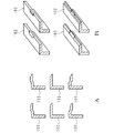
図17Aは、図13A、図13Bおよび図13Cに示す3通りのハウジング102の基本断面形状と、図14Aおよび図14Bに示す2通りのコーナー処理形状とを組み合わせた、6通りのハウジング102の断面形状の例を示す模式断面図である。図17Aの上側に示す2個の図は、図13Bに記載したハウジング102の形状の例を示す。図17Aの中央の2個の図は、図13Aに記載したハウジング102の形状の例を示す。図17Aの下側の2個の図は、図13Cに記載したハウジング102の形状の例を示す。図17Aの左側の3個の図は、図14Aに記載したコーナー処理形状の例を示す。図17Aの右側の3個の図は、図14Bに記載したコーナー処理形状の例を示す。
FIG. 17A shows a cross section of the six
図17Bは、図14Aおよび図14Bに示す2通りのコーナー処理形状と、図15および図16に示すコーナー処理の配置方法とを組み合わせた、4通りのハウジング102の部分拡大斜視図の例を示す模式斜視図である。図17Bの左上の図は、図14Aに記載したコーナー処理形状を、図15に示す配置方法で配置した例を示す。図17Bの右上の図は、図14Bに記載したコーナー処理形状を、図15に示す配置方法で配置した例を示す。図17Bの左下の図は、図14Aに記載したコーナー処理形状を、図16Aに示す配置方法で配置した例を示す。図17Bの右下の図は、図14Bに記載したコーナー処理形状を、図16Bに示す配置方法で配置した例を示す。
FIG. 17B shows an example of a partially enlarged perspective view of the four
それぞれの形状の場合に使用する、UV硬化型等のエネルギー線硬化型のダム材およびOCR104について、物性的な制約は無い。さらには、湿気硬化型、熱硬化型、二液硬化型、これらの硬化方式が複合した複合硬化型の樹脂等の、エネルギー線硬化型に比べて硬化に時間を要する樹脂を採用する場合であっても、UV硬化樹脂と同様の効果を得ることができる。いずれの樹脂材料を使用する場合であっても、ハウジング102の開口端部に端掛けを行った状態で樹脂ダム105を形成することにより、耐荷重を増す効果を得ることができる。
There are no physical restrictions on the energy ray-curable dam material such as UV curable and OCR104 used for each shape. Furthermore, there is a case where a resin that takes longer to cure than the energy ray curing type, such as a moisture curing type, a thermosetting type, a two-component curing type, and a composite curing type resin in which these curing methods are combined, is adopted. However, the same effect as that of the UV curable resin can be obtained. Regardless of which resin material is used, the effect of increasing the load capacity can be obtained by forming the
[実施の形態1]
次に、具体的な実施の形態について説明する。
[Embodiment 1]
Next, a specific embodiment will be described.
図1は実施の形態1の表示装置の構成を示す図である。一般的な表示モジュール103は、上下基板(液晶表示パネル)100がケース部(バックライト)101とハウジング(金属ベゼル)102との間に組み込まれた構成である。表示モジュール103の表示面をワークとして、ハウジング102の開口端部に沿って全周に、UV硬化型の樹脂材料製の樹脂ダム105により隙間なくシールが施されている。樹脂ダム105で囲まれた表示面に、OCR104が均一の厚さで塗布されている。OCR104を介して上下基板100の表示面と前面パネル(タッチパネル)106とが貼り合わされている。ハウジング102の厚みは、10.4型以下の表示装置であれば0.4ミリメートル程度、19型以上の表示装置であれば1ミリメートル程度である。
FIG. 1 is a diagram showing a configuration of a display device according to the first embodiment. The
図18は、表示装置の模式断面図を示す。表示装置の断面を見た場合、ハウジング102と液晶表示パネル100との間には、0.2ミリメートル程度の隙間が空いている。ハウジング102の開口端部の上面(前面パネル106側の表面)に幅0.5ミリメートル、高さ0.3ミリメートル程度の樹脂ダム105材が液晶表示パネル100の表示面との間で端掛けされ、ハウジング102と樹脂ダム105とが乖離しないよう形成されている。
FIG. 18 shows a schematic cross-sectional view of the display device. Looking at the cross section of the display device, there is a gap of about 0.2 mm between the
図19は、斜面によるコーナー処理を、ハウジング102の樹脂ダム接合部504に対応する部分に施した例を示す模式部分拡大斜視図である。図20は、L字面によるコーナー処理を、ハウジング102の樹脂ダム接合部504に対応する部分に施した例を示す模式部分拡大斜視図である。図19および図20に示すように、樹脂ダム接合部504に対応する部分のハウジング102にコーナー処理を施すことにより、膨らみ508を抑えることができる。そのため、膨らみ508に起因する表示異常の発生を抑制できる。
FIG. 19 is a schematic partial enlarged perspective view showing an example in which a corner treatment by a slope is applied to a portion of the
図21は、図19および図20に示す形状における樹脂ダム接合部504の脹らみ508の適合性を説明する図である。図21Aから図21Eは、膨らみ508の形状の異なる5種類の例を示す。図21の各図の上側は、図19および図20に示す斜視図を図中上側から見た上面図である。図21の各図の下側は、図19および図20に示す斜視図を図中右側から見た側面図である。
FIG. 21 is a diagram illustrating the suitability of the
図21Aは、膨らみ508が周囲より高いため不適合である。図21B、図21Cおよび図21Dは膨らみ508が周囲よりも低く、凹みが照射不能域501へ通じていないため、適合である。図21Eは、凹みが照射不能域501へ通じているため不適合である。
FIG. 21A is incompatible because the
図19および図20に示すように、ハウジング102の樹脂ダム接合部504に対応しる部分に部分的にコーナー処理を施すことで、樹脂ダム105の膨らみ508の高さを低減することができる。例えば、不適合である図12Bと同程度の樹脂ダム105の膨らみ508の高さを、図21Bに示す程度にまで軽減することにより、適合の状態にすることが可能になる。その結果、表示パネル100の表示異常の発生を抑制することができる。
As shown in FIGS. 19 and 20, the height of the
本実施の形態によると、樹脂ダム接合部504の膨らみ508を小さくすることができる。そのため、樹脂ダム接合部504の膨らみ508に起因する上下基板100の表示異常の発生を防止することができる。
According to this embodiment, the
本実施の形態のハウジング102は、前面パネル106の貼り合せが不要な表示モジュール製品との共用も可能であるので、開発費用と開発期間を圧縮できる。
Since the
なお、本願発明者らの実験によると、ハウジング102開口端部に樹脂ダム105を接触させただけの形状(図8A参照)と比較して、ハウジング102上面に樹脂ダム105を端掛けした形状(図18参照)では、2倍以上の強度が得られることが確認された。したがって、ハウジングイン方式で表示モジュール103と前面パネル106とを樹脂ダム105材およびOCR104を用いて貼り合せる場合には、樹脂ダム105は、図18に示すような端掛け構造であることが望ましい。さらに表示異常の誘発を防止するために、樹脂ダム105はハウジング102の開口端部に凹凸少なく形成されていることが望ましい。
According to the experiments by the inventors of the present application, the shape in which the
前述した通り、ハウジングイン方式の場合にはUV照射不能域501が存在する。したがって、UV照射不能域501へ通じるパスが樹脂ダム105に有ってはならない。UV照射不能域501へ通じるパスが存在する不適合な樹脂ダム105の形状の例を示す模式断面図を、図22に示す。図22Aに示す例では、樹脂ダム105と上下基板100の間にパスが有る。図22Bに示す例では、樹脂ダム105とハウジング102の間にパスが有る。図22Cに示す例では、樹脂ダム105の間にパスが有る。
As described above, in the case of the housing-in method, there is a UV irradiation
[実施の形態2]
図10に示すように、樹脂ダム105をハウジング102開口端部に接触させるだけの場合には、必要最小限の量のOCR104を使用して製造することが可能である。しかし図18に示すように、ハウジング102上面に樹脂ダム105を端掛けする場合は、樹脂ダム105の高さが0.3ミリメートル(20〜30パーセント)程度高くなる。そのため、製造に必要なOCR104の量が増えて、製造コストが上がってしまう。本実施の形態は、このような課題を緩和または解消することが可能な、ハウジング102の開口端部の形状に関する。実施の形態1と共通する部分については説明を省略する。
[Embodiment 2]
As shown in FIG. 10, when the
図16は、本実施の形態のハウジング102の形状を示す図である。本実施の形態は、ハウジング102が厚い場合(0.6ミリメートル程度以上)に適している。ハウジング102の樹脂ダム接合部504に対応する位置に部分的にコーナー処理を施した上で、さらにハウジング102の開口端部の全周にわたって複合してコーナー処理を施している。
FIG. 16 is a diagram showing the shape of the
本実施の形態によると、樹脂ダム接合部504の膨らみ508を抑制することによる表示品質の改善が可能である。また、樹脂ダム105の高さを低くすることによってダム材およびOCR104の使用量を削減することによる、製造コストの低減も可能である。
According to this embodiment, it is possible to improve the display quality by suppressing the
図16Aは、斜面による全周のコーナー処理(図14A参照)を施した上で、さらに樹脂ダム接合部504に対応する位置に斜面による部分的なコーナー処理(図14A参照)を施したハウジング102の例を示す。図16Bは、L字面による全周のコーナー処理(図14B参照)を施した上で、さらに樹脂ダム接合部504に対応する位置にL字面による部分的なコーナー処理(図14B参照)を施した例を示す。
FIG. 16A shows the
なお、全周のコーナー処理の形状と樹脂ダム接合部504に対応した部分的なコーナー処理の形状とを、一致させる必要は無い。ハウジング102の材質、形状、厚み等に応じて、図14Aから図14Dに示す形状等を種々組み合わせて選択することが可能である。
It is not necessary to match the shape of the corner treatment on the entire circumference with the shape of the partial corner treatment corresponding to the resin dam
[実施の形態3]
実施の形態1および実施の形態2では、表示モジュール103と前面パネル106とをOCR104を介して貼り合せるオプティカルボンディングの場合について説明した。本実施の形態は、表示モジュール103と前面パネル106とを空気層107を介して貼り合せるエアギャップボンディング構造の表示装置に関する。実施の形態1と共通する部分については説明を省略する。
[Embodiment 3]
In the first embodiment and the second embodiment, the case of opticarboning in which the
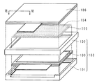
図23は実施の形態3の表示装置の構成を示す模式分解斜視図である。図24は、実施の形態3の表示装置の模式断面図である。表示モジュール103と前面パネル106との間に、空気層107が存在する。ハウジング102と前面パネル106とは、両面テープ108により貼り合わされている。樹脂ダム105は空気層107へ異物が侵入することを防止するために設けられている。
FIG. 23 is a schematic exploded perspective view showing the configuration of the display device according to the third embodiment. FIG. 24 is a schematic cross-sectional view of the display device of the third embodiment. An
本実施の形態においては、実施の形態1および実施の形態2と同様に、樹脂ダム接合部504の膨らみ508を低くすることにより表示異常を防止することができる。また、樹脂ダム105をハウジング102の開口端部に端掛けるように構成することにより、ハウジング102から乖離しにくい樹脂ダム105を作製することができる。これにより、表示面内への異物侵入による表示品質の低下を防止することができる。
In the present embodiment, as in the first and second embodiments, the display abnormality can be prevented by lowering the
各実施例で記載されている技術的特徴(構成要件)はお互いに組合せ可能であり、組み合わせすることにより、新しい技術的特徴を形成することができる。
今回開示された実施の形態はすべての点で例示であって、制限的なものでは無いと考えられるべきである。本発明の範囲は、上記した意味では無く、特許請求の範囲によって示され、特許請求の範囲と均等の意味および範囲内でのすべての変更が含まれることが意図される。
The technical features (constituent requirements) described in each embodiment can be combined with each other, and by combining them, a new technical feature can be formed.
The embodiments disclosed this time should be considered as exemplary in all respects and not restrictive. The scope of the present invention is indicated by the scope of claims, not the above-mentioned meaning, and is intended to include all modifications within the meaning and scope equivalent to the scope of claims.
100 上下基板(表示パネル、液晶表示パネル)
101 ケース部
102 ハウジング(金属ベゼル)
103 表示モジュール
104 透明樹脂(光学弾性樹脂、OCR)
105 樹脂部材(樹脂ダム)
106 前面パネル(透光性基板、タッチパネル)
107 空気層
108 両面テープ(貼り合せ部材)
300 ディスペンス装置
301 紫外線ランプ
302 強力紫外線ランプ
500 加工面
501 UV照射不能域
502 形成開始端
503 形成終了端
504 樹脂ダム接合部
505 表面基準線
506 側面基準線
507 樹脂ダムの高さ
508 脹らみ
100 Upper and lower boards (display panel, liquid crystal display panel)
101
103
105 Resin member (resin dam)
106 Front panel (translucent board, touch panel)
107
300
Claims (9)
前記ハウジングの開口の全周に沿って前記上下基板上に設けられており、形成開始端と形成終了端とが前記開口の周方向に重なって他の部分に比べて膨らんだ接合部を有する樹脂部材と、
前記樹脂部材を挟んで前記表示モジュールと対向する前面パネルとを有し、
前記ハウジングは、前記上下基板と前記前面パネルとの間に挟まれるように設けられ、さらに前記ハウジングの開口端部の稜線の前記接合部に対応する箇所に加工面が設けられており、
前記樹脂部材は、前記ハウジングの開口端部の全周に接触し、なおかつ前記ハウジングの上面に端掛けされるように設けられている
ことを特徴とする表示装置。 A display module including a bonded upper and lower boards, a case portion for accommodating the upper and lower boards, and a housing having an open display portion.
Wherein and wherein provided on the upper and lower substrates along the entire periphery of the opening of the housing, the formation start end and the completion of forming end joints swollen than circumferentially heavy Do I other portion of said opening With the resin member
It has a front panel facing the display module with the resin member interposed therebetween.
The housing is provided so as to be sandwiched between the upper and lower substrates and the front panel, and a machined surface is provided at a portion corresponding to the joint portion of the ridgeline of the open end portion of the housing.
A display device characterized in that the resin member is provided so as to be in contact with the entire circumference of an open end portion of the housing and to be end-mounted on the upper surface of the housing.
前記表示モジュールと前記前面パネルとが前記樹脂部材と前記透明樹脂とを介して貼合されている
ことを特徴とする請求項1に記載の表示装置。 Further having a transparent resin on the upper and lower substrates inside the resin member,
The display device according to claim 1, wherein the display module and the front panel are bonded to each other via the resin member and the transparent resin.
ことを特徴とする請求項2に記載の表示装置。 The display device according to claim 2, wherein the transparent resin material comprises an energy ray-curable type, a moisture-curable type, a thermosetting type, a two-component curable type, or a composite material thereof.
ことを特徴とする請求項1から請求項3のいずれか一つに記載の表示装置。 The display device according to any one of claims 1 to 3, wherein the machined surface is a slope, an L-shaped surface, a concave curved surface, or a convex curved surface.
ことを特徴とする請求項1から請求項4のいずれか一つに記載の表示装置。 The display device according to any one of claims 1 to 4, wherein the processed surface is provided corresponding to a joint portion of the resin member at an open end portion of the housing.
ことを特徴とする請求項1から請求項6のいずれか一つに記載の表示装置。 The cross-sectional shape of the machined surface is any one of claims 1 to 6, characterized in that the cross-sectional shape of the open end portion is recessed inward from the front panel side surface and the side surface. The display device described.
ことを特徴とする請求項1から請求項7のいずれか一つに記載の表示装置。 The material of the resin member is any one of claims 1 to 7, wherein the material is an energy ray-curable type, a moisture-curable type, a thermosetting type, a two-component curable type, or a composite material thereof. The display device described.
前記ハウジングの開口端部の稜線の一部に設けられた加工面を始点および終点として、前記加工面において形成開始端と形成終了端とが前記開口端部の周方向に重なって他の部分に比べて膨らんだ接合部を形成し、かつ前記ハウジングの上面に端掛けされるように、流動性を備える樹脂を前記開口の全周に沿って塗布し、
前記樹脂を挟んで前記表示モジュールと対向する前面パネルを配置する
ことを特徴とする表示装置の製造方法。 A display module including the bonded upper and lower substrates, a case portion for accommodating the upper and lower substrates, and a housing having an open display portion is arranged with the housing facing up.
The working surface provided on a portion of the ridge line of the open end of the housing as a start point and an end point, the formation starting end and formed finish end in the machined surface of the circumferential heavy Do I other said open end A fluid resin is applied along the entire circumference of the opening so as to form a joint portion that bulges compared to the portion and is end-mounted on the upper surface of the housing.
A method for manufacturing a display device, which comprises arranging a front panel facing the display module with the resin sandwiched between them.
Priority Applications (3)
| Application Number | Priority Date | Filing Date | Title |
|---|---|---|---|
| JP2016111987A JP6870164B2 (en) | 2016-06-03 | 2016-06-03 | Display device and manufacturing method of display device |
| CN201710407911.XA CN107463017B (en) | 2016-06-03 | 2017-06-02 | Display device and method of manufacturing the same |
| US15/611,862 US10234709B2 (en) | 2016-06-03 | 2017-06-02 | Display apparatus and method of manufacturing the same |
Applications Claiming Priority (1)
| Application Number | Priority Date | Filing Date | Title |
|---|---|---|---|
| JP2016111987A JP6870164B2 (en) | 2016-06-03 | 2016-06-03 | Display device and manufacturing method of display device |
Publications (3)
| Publication Number | Publication Date |
|---|---|
| JP2017219584A JP2017219584A (en) | 2017-12-14 |
| JP2017219584A5 JP2017219584A5 (en) | 2019-07-04 |
| JP6870164B2 true JP6870164B2 (en) | 2021-05-12 |
Family
ID=60483188
Family Applications (1)
| Application Number | Title | Priority Date | Filing Date |
|---|---|---|---|
| JP2016111987A Active JP6870164B2 (en) | 2016-06-03 | 2016-06-03 | Display device and manufacturing method of display device |
Country Status (3)
| Country | Link |
|---|---|
| US (1) | US10234709B2 (en) |
| JP (1) | JP6870164B2 (en) |
| CN (1) | CN107463017B (en) |
Families Citing this family (3)
| Publication number | Priority date | Publication date | Assignee | Title |
|---|---|---|---|---|
| KR102750572B1 (en) * | 2017-01-06 | 2025-01-07 | 삼성디스플레이 주식회사 | Display Apparatus |
| JP2021096423A (en) * | 2019-12-19 | 2021-06-24 | 株式会社デンソー | Vehicle display device |
| CN115698916A (en) * | 2021-05-31 | 2023-02-03 | 京东方科技集团股份有限公司 | display device |
Family Cites Families (15)
| Publication number | Priority date | Publication date | Assignee | Title |
|---|---|---|---|---|
| JP3979914B2 (en) * | 2002-10-09 | 2007-09-19 | シャープ株式会社 | Method for manufacturing liquid crystal panel unit and method for manufacturing liquid crystal display device |
| KR20060022164A (en) * | 2004-09-06 | 2006-03-09 | 삼성전자주식회사 | A storage container for a display device, a liquid crystal display device having the storage container and a manufacturing method of the liquid crystal display device |
| JP5044830B2 (en) * | 2007-03-08 | 2012-10-10 | 株式会社ジャパンディスプレイウェスト | Electro-optical device and electronic apparatus |
| KR101445897B1 (en) * | 2007-04-04 | 2014-09-29 | 데쿠세리아루즈 가부시키가이샤 | Manufacturing method of image display device |
| JP5155826B2 (en) * | 2007-12-27 | 2013-03-06 | セイコーインスツル株式会社 | Manufacturing method of display device |
| US20090183819A1 (en) | 2007-12-27 | 2009-07-23 | Tsutomu Matsuhira | Manufacturing method for a display device |
| JP5142854B2 (en) * | 2008-06-25 | 2013-02-13 | 株式会社ジャパンディスプレイイースト | Display device and manufacturing method thereof |
| JP5451015B2 (en) * | 2008-09-12 | 2014-03-26 | 協立化学産業株式会社 | Display panel manufacturing method and display panel |
| JP2013076934A (en) * | 2011-09-30 | 2013-04-25 | Shibaura Mechatronics Corp | Bonding structure and manufacturing method of the same |
| JP2013088455A (en) * | 2011-10-13 | 2013-05-13 | Kaneka Corp | Image display device, manufacturing method of the same, and electric/electronic device |
| CN103853366B (en) * | 2012-11-29 | 2017-07-11 | 宸鸿科技(厦门)有限公司 | Apply the adhesive layer and preparation method thereof in contact panel |
| JP6292477B2 (en) * | 2013-09-07 | 2018-03-14 | Tianma Japan株式会社 | Display device |
| JP6324045B2 (en) * | 2013-12-04 | 2018-05-16 | 三菱電機株式会社 | Display device |
| JP6494920B2 (en) * | 2014-04-07 | 2019-04-03 | 三菱電機株式会社 | Manufacturing method of image display device |
| JP6406952B2 (en) * | 2014-09-19 | 2018-10-17 | 三菱電機株式会社 | Display device |
-
2016
- 2016-06-03 JP JP2016111987A patent/JP6870164B2/en active Active
-
2017
- 2017-06-02 CN CN201710407911.XA patent/CN107463017B/en active Active
- 2017-06-02 US US15/611,862 patent/US10234709B2/en active Active
Also Published As
| Publication number | Publication date |
|---|---|
| US20170351136A1 (en) | 2017-12-07 |
| JP2017219584A (en) | 2017-12-14 |
| US10234709B2 (en) | 2019-03-19 |
| CN107463017A (en) | 2017-12-12 |
| CN107463017B (en) | 2021-11-02 |
Similar Documents
| Publication | Publication Date | Title |
|---|---|---|
| JP6566297B2 (en) | Display device and manufacturing method thereof | |
| EP2485082B1 (en) | Liquid crystal display device | |
| EP2246730B1 (en) | Liquid crystal display device | |
| CN101387769B (en) | Display device | |
| JP5370240B2 (en) | Display module | |
| CN103376574B (en) | Display device and manufacture method thereof | |
| KR20120044501A (en) | Display device having a touch screen panel and manufacturing method of the same | |
| KR20150059586A (en) | Structure of amoled module and method for assembling the same | |
| JP6494920B2 (en) | Manufacturing method of image display device | |
| US20170285819A1 (en) | Display Panel, Manufacturing Method Thereof and Display Device | |
| TWI486680B (en) | Liquid crystal display device and manufacturing method thereof | |
| KR20160053923A (en) | Capacitive touch panel | |
| JP6870164B2 (en) | Display device and manufacturing method of display device | |
| JP2016194670A (en) | Display device and manufacturing method of display device | |
| JP2014182164A (en) | Display device | |
| TW201627166A (en) | Optical adhesive, panel, and method for bonding substrates | |
| WO2022178664A9 (en) | Display module and manufacturing method therefor, and display device | |
| JP2005107165A (en) | Liquid crystal display device and method of manufacturing liquid crystal display device | |
| US20160274411A1 (en) | Liquid crystal display apparatus and method for fabricating the same | |
| US11090906B2 (en) | Apparatus and manufacturing method thereof | |
| EP3674784B1 (en) | Display manufacturing device and display manufacturing method | |
| JP6739565B2 (en) | Image display | |
| JP2017198763A (en) | Image display panel having front plate and method for manufacturing the same | |
| TWI706202B (en) | Display panel | |
| WO2026020282A1 (en) | Housing assembly, manufacturing method for housing assembly, and device having housing assembly |
Legal Events
| Date | Code | Title | Description |
|---|---|---|---|
| A521 | Request for written amendment filed |
Free format text: JAPANESE INTERMEDIATE CODE: A523 Effective date: 20190528 |
|
| A621 | Written request for application examination |
Free format text: JAPANESE INTERMEDIATE CODE: A621 Effective date: 20190528 |
|
| A711 | Notification of change in applicant |
Free format text: JAPANESE INTERMEDIATE CODE: A711 Effective date: 20191108 |
|
| A521 | Request for written amendment filed |
Free format text: JAPANESE INTERMEDIATE CODE: A523 Effective date: 20200117 |
|
| A977 | Report on retrieval |
Free format text: JAPANESE INTERMEDIATE CODE: A971007 Effective date: 20200318 |
|
| A131 | Notification of reasons for refusal |
Free format text: JAPANESE INTERMEDIATE CODE: A131 Effective date: 20200331 |
|
| A521 | Request for written amendment filed |
Free format text: JAPANESE INTERMEDIATE CODE: A523 Effective date: 20200624 |
|
| A131 | Notification of reasons for refusal |
Free format text: JAPANESE INTERMEDIATE CODE: A131 Effective date: 20200811 |
|
| A521 | Request for written amendment filed |
Free format text: JAPANESE INTERMEDIATE CODE: A523 Effective date: 20201106 |
|
| TRDD | Decision of grant or rejection written | ||
| A01 | Written decision to grant a patent or to grant a registration (utility model) |
Free format text: JAPANESE INTERMEDIATE CODE: A01 Effective date: 20210209 |
|
| A61 | First payment of annual fees (during grant procedure) |
Free format text: JAPANESE INTERMEDIATE CODE: A61 Effective date: 20210308 |
|
| R150 | Certificate of patent or registration of utility model |
Ref document number: 6870164 Country of ref document: JP Free format text: JAPANESE INTERMEDIATE CODE: R150 |
|
| R250 | Receipt of annual fees |
Free format text: JAPANESE INTERMEDIATE CODE: R250 |
|
| R250 | Receipt of annual fees |
Free format text: JAPANESE INTERMEDIATE CODE: R250 |
|
| R250 | Receipt of annual fees |
Free format text: JAPANESE INTERMEDIATE CODE: R250 |