JP6870164B2 - 表示装置および表示装置の製造方法 - Google Patents
表示装置および表示装置の製造方法 Download PDFInfo
- Publication number
- JP6870164B2 JP6870164B2 JP2016111987A JP2016111987A JP6870164B2 JP 6870164 B2 JP6870164 B2 JP 6870164B2 JP 2016111987 A JP2016111987 A JP 2016111987A JP 2016111987 A JP2016111987 A JP 2016111987A JP 6870164 B2 JP6870164 B2 JP 6870164B2
- Authority
- JP
- Japan
- Prior art keywords
- housing
- display device
- resin
- display
- front panel
- Prior art date
- Legal status (The legal status is an assumption and is not a legal conclusion. Google has not performed a legal analysis and makes no representation as to the accuracy of the status listed.)
- Active
Links
Images






Classifications
-
- G—PHYSICS
- G02—OPTICS
- G02F—OPTICAL DEVICES OR ARRANGEMENTS FOR THE CONTROL OF LIGHT BY MODIFICATION OF THE OPTICAL PROPERTIES OF THE MEDIA OF THE ELEMENTS INVOLVED THEREIN; NON-LINEAR OPTICS; FREQUENCY-CHANGING OF LIGHT; OPTICAL LOGIC ELEMENTS; OPTICAL ANALOGUE/DIGITAL CONVERTERS
- G02F1/00—Devices or arrangements for the control of the intensity, colour, phase, polarisation or direction of light arriving from an independent light source, e.g. switching, gating or modulating; Non-linear optics
- G02F1/01—Devices or arrangements for the control of the intensity, colour, phase, polarisation or direction of light arriving from an independent light source, e.g. switching, gating or modulating; Non-linear optics for the control of the intensity, phase, polarisation or colour
- G02F1/13—Devices or arrangements for the control of the intensity, colour, phase, polarisation or direction of light arriving from an independent light source, e.g. switching, gating or modulating; Non-linear optics for the control of the intensity, phase, polarisation or colour based on liquid crystals, e.g. single liquid crystal display cells
- G02F1/133—Constructional arrangements; Operation of liquid crystal cells; Circuit arrangements
- G02F1/1333—Constructional arrangements; Manufacturing methods
- G02F1/133308—Support structures for LCD panels, e.g. frames or bezels
-
- G—PHYSICS
- G02—OPTICS
- G02B—OPTICAL ELEMENTS, SYSTEMS OR APPARATUS
- G02B1/00—Optical elements characterised by the material of which they are made; Optical coatings for optical elements
- G02B1/04—Optical elements characterised by the material of which they are made; Optical coatings for optical elements made of organic materials, e.g. plastics
-
- G—PHYSICS
- G02—OPTICS
- G02F—OPTICAL DEVICES OR ARRANGEMENTS FOR THE CONTROL OF LIGHT BY MODIFICATION OF THE OPTICAL PROPERTIES OF THE MEDIA OF THE ELEMENTS INVOLVED THEREIN; NON-LINEAR OPTICS; FREQUENCY-CHANGING OF LIGHT; OPTICAL LOGIC ELEMENTS; OPTICAL ANALOGUE/DIGITAL CONVERTERS
- G02F1/00—Devices or arrangements for the control of the intensity, colour, phase, polarisation or direction of light arriving from an independent light source, e.g. switching, gating or modulating; Non-linear optics
- G02F1/01—Devices or arrangements for the control of the intensity, colour, phase, polarisation or direction of light arriving from an independent light source, e.g. switching, gating or modulating; Non-linear optics for the control of the intensity, phase, polarisation or colour
- G02F1/13—Devices or arrangements for the control of the intensity, colour, phase, polarisation or direction of light arriving from an independent light source, e.g. switching, gating or modulating; Non-linear optics for the control of the intensity, phase, polarisation or colour based on liquid crystals, e.g. single liquid crystal display cells
- G02F1/133—Constructional arrangements; Operation of liquid crystal cells; Circuit arrangements
- G02F1/1333—Constructional arrangements; Manufacturing methods
- G02F1/1343—Electrodes
- G02F1/13439—Electrodes characterised by their electrical, optical, physical properties; materials therefor; method of making
-
- G—PHYSICS
- G02—OPTICS
- G02F—OPTICAL DEVICES OR ARRANGEMENTS FOR THE CONTROL OF LIGHT BY MODIFICATION OF THE OPTICAL PROPERTIES OF THE MEDIA OF THE ELEMENTS INVOLVED THEREIN; NON-LINEAR OPTICS; FREQUENCY-CHANGING OF LIGHT; OPTICAL LOGIC ELEMENTS; OPTICAL ANALOGUE/DIGITAL CONVERTERS
- G02F1/00—Devices or arrangements for the control of the intensity, colour, phase, polarisation or direction of light arriving from an independent light source, e.g. switching, gating or modulating; Non-linear optics
- G02F1/01—Devices or arrangements for the control of the intensity, colour, phase, polarisation or direction of light arriving from an independent light source, e.g. switching, gating or modulating; Non-linear optics for the control of the intensity, phase, polarisation or colour
- G02F1/13—Devices or arrangements for the control of the intensity, colour, phase, polarisation or direction of light arriving from an independent light source, e.g. switching, gating or modulating; Non-linear optics for the control of the intensity, phase, polarisation or colour based on liquid crystals, e.g. single liquid crystal display cells
- G02F1/133—Constructional arrangements; Operation of liquid crystal cells; Circuit arrangements
- G02F1/136—Liquid crystal cells structurally associated with a semi-conducting layer or substrate, e.g. cells forming part of an integrated circuit
-
- H—ELECTRICITY
- H10—SEMICONDUCTOR DEVICES; ELECTRIC SOLID-STATE DEVICES NOT OTHERWISE PROVIDED FOR
- H10K—ORGANIC ELECTRIC SOLID-STATE DEVICES
- H10K50/00—Organic light-emitting devices
- H10K50/80—Constructional details
- H10K50/84—Passivation; Containers; Encapsulations
- H10K50/842—Containers
- H10K50/8426—Peripheral sealing arrangements, e.g. adhesives, sealants
-
- H—ELECTRICITY
- H10—SEMICONDUCTOR DEVICES; ELECTRIC SOLID-STATE DEVICES NOT OTHERWISE PROVIDED FOR
- H10K—ORGANIC ELECTRIC SOLID-STATE DEVICES
- H10K50/00—Organic light-emitting devices
- H10K50/80—Constructional details
- H10K50/84—Passivation; Containers; Encapsulations
- H10K50/844—Encapsulations
-
- H—ELECTRICITY
- H10—SEMICONDUCTOR DEVICES; ELECTRIC SOLID-STATE DEVICES NOT OTHERWISE PROVIDED FOR
- H10K—ORGANIC ELECTRIC SOLID-STATE DEVICES
- H10K50/00—Organic light-emitting devices
- H10K50/80—Constructional details
- H10K50/85—Arrangements for extracting light from the devices
- H10K50/858—Arrangements for extracting light from the devices comprising refractive means, e.g. lenses
-
- H—ELECTRICITY
- H10—SEMICONDUCTOR DEVICES; ELECTRIC SOLID-STATE DEVICES NOT OTHERWISE PROVIDED FOR
- H10K—ORGANIC ELECTRIC SOLID-STATE DEVICES
- H10K59/00—Integrated devices, or assemblies of multiple devices, comprising at least one organic light-emitting element covered by group H10K50/00
- H10K59/80—Constructional details
- H10K59/87—Passivation; Containers; Encapsulations
- H10K59/871—Self-supporting sealing arrangements
- H10K59/8722—Peripheral sealing arrangements, e.g. adhesives, sealants
-
- H—ELECTRICITY
- H10—SEMICONDUCTOR DEVICES; ELECTRIC SOLID-STATE DEVICES NOT OTHERWISE PROVIDED FOR
- H10K—ORGANIC ELECTRIC SOLID-STATE DEVICES
- H10K71/00—Manufacture or treatment specially adapted for the organic devices covered by this subclass
- H10K71/50—Forming devices by joining two substrates together, e.g. lamination techniques
-
- G—PHYSICS
- G02—OPTICS
- G02F—OPTICAL DEVICES OR ARRANGEMENTS FOR THE CONTROL OF LIGHT BY MODIFICATION OF THE OPTICAL PROPERTIES OF THE MEDIA OF THE ELEMENTS INVOLVED THEREIN; NON-LINEAR OPTICS; FREQUENCY-CHANGING OF LIGHT; OPTICAL LOGIC ELEMENTS; OPTICAL ANALOGUE/DIGITAL CONVERTERS
- G02F1/00—Devices or arrangements for the control of the intensity, colour, phase, polarisation or direction of light arriving from an independent light source, e.g. switching, gating or modulating; Non-linear optics
- G02F1/01—Devices or arrangements for the control of the intensity, colour, phase, polarisation or direction of light arriving from an independent light source, e.g. switching, gating or modulating; Non-linear optics for the control of the intensity, phase, polarisation or colour
- G02F1/13—Devices or arrangements for the control of the intensity, colour, phase, polarisation or direction of light arriving from an independent light source, e.g. switching, gating or modulating; Non-linear optics for the control of the intensity, phase, polarisation or colour based on liquid crystals, e.g. single liquid crystal display cells
- G02F1/133—Constructional arrangements; Operation of liquid crystal cells; Circuit arrangements
- G02F1/1333—Constructional arrangements; Manufacturing methods
- G02F1/133308—Support structures for LCD panels, e.g. frames or bezels
- G02F1/133311—Environmental protection, e.g. against dust or humidity
-
- G—PHYSICS
- G02—OPTICS
- G02F—OPTICAL DEVICES OR ARRANGEMENTS FOR THE CONTROL OF LIGHT BY MODIFICATION OF THE OPTICAL PROPERTIES OF THE MEDIA OF THE ELEMENTS INVOLVED THEREIN; NON-LINEAR OPTICS; FREQUENCY-CHANGING OF LIGHT; OPTICAL LOGIC ELEMENTS; OPTICAL ANALOGUE/DIGITAL CONVERTERS
- G02F1/00—Devices or arrangements for the control of the intensity, colour, phase, polarisation or direction of light arriving from an independent light source, e.g. switching, gating or modulating; Non-linear optics
- G02F1/01—Devices or arrangements for the control of the intensity, colour, phase, polarisation or direction of light arriving from an independent light source, e.g. switching, gating or modulating; Non-linear optics for the control of the intensity, phase, polarisation or colour
- G02F1/13—Devices or arrangements for the control of the intensity, colour, phase, polarisation or direction of light arriving from an independent light source, e.g. switching, gating or modulating; Non-linear optics for the control of the intensity, phase, polarisation or colour based on liquid crystals, e.g. single liquid crystal display cells
- G02F1/133—Constructional arrangements; Operation of liquid crystal cells; Circuit arrangements
- G02F1/1333—Constructional arrangements; Manufacturing methods
- G02F1/133308—Support structures for LCD panels, e.g. frames or bezels
- G02F1/13332—Front frames
-
- G—PHYSICS
- G02—OPTICS
- G02F—OPTICAL DEVICES OR ARRANGEMENTS FOR THE CONTROL OF LIGHT BY MODIFICATION OF THE OPTICAL PROPERTIES OF THE MEDIA OF THE ELEMENTS INVOLVED THEREIN; NON-LINEAR OPTICS; FREQUENCY-CHANGING OF LIGHT; OPTICAL LOGIC ELEMENTS; OPTICAL ANALOGUE/DIGITAL CONVERTERS
- G02F1/00—Devices or arrangements for the control of the intensity, colour, phase, polarisation or direction of light arriving from an independent light source, e.g. switching, gating or modulating; Non-linear optics
- G02F1/01—Devices or arrangements for the control of the intensity, colour, phase, polarisation or direction of light arriving from an independent light source, e.g. switching, gating or modulating; Non-linear optics for the control of the intensity, phase, polarisation or colour
- G02F1/13—Devices or arrangements for the control of the intensity, colour, phase, polarisation or direction of light arriving from an independent light source, e.g. switching, gating or modulating; Non-linear optics for the control of the intensity, phase, polarisation or colour based on liquid crystals, e.g. single liquid crystal display cells
- G02F1/133—Constructional arrangements; Operation of liquid crystal cells; Circuit arrangements
- G02F1/1333—Constructional arrangements; Manufacturing methods
- G02F1/133308—Support structures for LCD panels, e.g. frames or bezels
- G02F1/133325—Assembling processes
-
- G—PHYSICS
- G02—OPTICS
- G02F—OPTICAL DEVICES OR ARRANGEMENTS FOR THE CONTROL OF LIGHT BY MODIFICATION OF THE OPTICAL PROPERTIES OF THE MEDIA OF THE ELEMENTS INVOLVED THEREIN; NON-LINEAR OPTICS; FREQUENCY-CHANGING OF LIGHT; OPTICAL LOGIC ELEMENTS; OPTICAL ANALOGUE/DIGITAL CONVERTERS
- G02F1/00—Devices or arrangements for the control of the intensity, colour, phase, polarisation or direction of light arriving from an independent light source, e.g. switching, gating or modulating; Non-linear optics
- G02F1/01—Devices or arrangements for the control of the intensity, colour, phase, polarisation or direction of light arriving from an independent light source, e.g. switching, gating or modulating; Non-linear optics for the control of the intensity, phase, polarisation or colour
- G02F1/13—Devices or arrangements for the control of the intensity, colour, phase, polarisation or direction of light arriving from an independent light source, e.g. switching, gating or modulating; Non-linear optics for the control of the intensity, phase, polarisation or colour based on liquid crystals, e.g. single liquid crystal display cells
- G02F1/133—Constructional arrangements; Operation of liquid crystal cells; Circuit arrangements
- G02F1/1333—Constructional arrangements; Manufacturing methods
- G02F1/133308—Support structures for LCD panels, e.g. frames or bezels
- G02F1/133331—Cover glasses
-
- G—PHYSICS
- G02—OPTICS
- G02F—OPTICAL DEVICES OR ARRANGEMENTS FOR THE CONTROL OF LIGHT BY MODIFICATION OF THE OPTICAL PROPERTIES OF THE MEDIA OF THE ELEMENTS INVOLVED THEREIN; NON-LINEAR OPTICS; FREQUENCY-CHANGING OF LIGHT; OPTICAL LOGIC ELEMENTS; OPTICAL ANALOGUE/DIGITAL CONVERTERS
- G02F1/00—Devices or arrangements for the control of the intensity, colour, phase, polarisation or direction of light arriving from an independent light source, e.g. switching, gating or modulating; Non-linear optics
- G02F1/01—Devices or arrangements for the control of the intensity, colour, phase, polarisation or direction of light arriving from an independent light source, e.g. switching, gating or modulating; Non-linear optics for the control of the intensity, phase, polarisation or colour
- G02F1/13—Devices or arrangements for the control of the intensity, colour, phase, polarisation or direction of light arriving from an independent light source, e.g. switching, gating or modulating; Non-linear optics for the control of the intensity, phase, polarisation or colour based on liquid crystals, e.g. single liquid crystal display cells
- G02F1/133—Constructional arrangements; Operation of liquid crystal cells; Circuit arrangements
- G02F1/1333—Constructional arrangements; Manufacturing methods
- G02F1/13338—Input devices, e.g. touch panels
-
- G—PHYSICS
- G02—OPTICS
- G02F—OPTICAL DEVICES OR ARRANGEMENTS FOR THE CONTROL OF LIGHT BY MODIFICATION OF THE OPTICAL PROPERTIES OF THE MEDIA OF THE ELEMENTS INVOLVED THEREIN; NON-LINEAR OPTICS; FREQUENCY-CHANGING OF LIGHT; OPTICAL LOGIC ELEMENTS; OPTICAL ANALOGUE/DIGITAL CONVERTERS
- G02F2202/00—Materials and properties
- G02F2202/28—Adhesive materials or arrangements
Landscapes
- Physics & Mathematics (AREA)
- Nonlinear Science (AREA)
- Optics & Photonics (AREA)
- General Physics & Mathematics (AREA)
- Mathematical Physics (AREA)
- Chemical & Material Sciences (AREA)
- Crystallography & Structural Chemistry (AREA)
- Engineering & Computer Science (AREA)
- Manufacturing & Machinery (AREA)
- Microelectronics & Electronic Packaging (AREA)
- Devices For Indicating Variable Information By Combining Individual Elements (AREA)
- Liquid Crystal (AREA)
Description
次に、具体的な実施の形態について説明する。
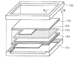
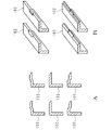
図10に示すように、樹脂ダム105をハウジング102開口端部に接触させるだけの場合には、必要最小限の量のOCR104を使用して製造することが可能である。しかし図18に示すように、ハウジング102上面に樹脂ダム105を端掛けする場合は、樹脂ダム105の高さが0.3ミリメートル(20〜30パーセント)程度高くなる。そのため、製造に必要なOCR104の量が増えて、製造コストが上がってしまう。本実施の形態は、このような課題を緩和または解消することが可能な、ハウジング102の開口端部の形状に関する。実施の形態1と共通する部分については説明を省略する。
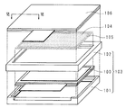
実施の形態1および実施の形態2では、表示モジュール103と前面パネル106とをOCR104を介して貼り合せるオプティカルボンディングの場合について説明した。本実施の形態は、表示モジュール103と前面パネル106とを空気層107を介して貼り合せるエアギャップボンディング構造の表示装置に関する。実施の形態1と共通する部分については説明を省略する。
今回開示された実施の形態はすべての点で例示であって、制限的なものでは無いと考えられるべきである。本発明の範囲は、上記した意味では無く、特許請求の範囲によって示され、特許請求の範囲と均等の意味および範囲内でのすべての変更が含まれることが意図される。
101 ケース部
102 ハウジング(金属ベゼル)
103 表示モジュール
104 透明樹脂(光学弾性樹脂、OCR)
105 樹脂部材(樹脂ダム)
106 前面パネル(透光性基板、タッチパネル)
107 空気層
108 両面テープ(貼り合せ部材)
300 ディスペンス装置
301 紫外線ランプ
302 強力紫外線ランプ
500 加工面
501 UV照射不能域
502 形成開始端
503 形成終了端
504 樹脂ダム接合部
505 表面基準線
506 側面基準線
507 樹脂ダムの高さ
508 脹らみ
Claims (9)
- 貼合された上下基板と、前記上下基板を収納するケース部と、表示部が開口しているハウジングとを含む表示モジュールと、
前記ハウジングの開口の全周に沿って前記上下基板上に設けられており、形成開始端と形成終了端とが前記開口の周方向に重なって他の部分に比べて膨らんだ接合部を有する樹脂部材と、
前記樹脂部材を挟んで前記表示モジュールと対向する前面パネルとを有し、
前記ハウジングは、前記上下基板と前記前面パネルとの間に挟まれるように設けられ、さらに前記ハウジングの開口端部の稜線の前記接合部に対応する箇所に加工面が設けられており、
前記樹脂部材は、前記ハウジングの開口端部の全周に接触し、なおかつ前記ハウジングの上面に端掛けされるように設けられている
ことを特徴とする表示装置。 - 前記樹脂部材の内側の前記上下基板上にさらに透明樹脂を有し、
前記表示モジュールと前記前面パネルとが前記樹脂部材と前記透明樹脂とを介して貼合されている
ことを特徴とする請求項1に記載の表示装置。 - 前記透明樹脂の材料は、エネルギー線硬化型、湿気硬化型、熱硬化型もしくは二液硬化型またはこれらが複合した材料からなる
ことを特徴とする請求項2に記載の表示装置。 - 前記加工面は、斜面、L字面、凹曲面または凸曲面である
ことを特徴とする請求項1から請求項3のいずれか一つに記載の表示装置。 - 前記加工面は、前記ハウジングの開口端部の前記樹脂部材の接合部に対応して設けられている
ことを特徴とする請求項1から請求項4のいずれか一つに記載の表示装置。 - 前記加工面は、さらに前記ハウジングの開口端部の全周囲に複合して設けられていることを特徴とする請求項1から請求項5のいずれか一つに記載の表示装置。
- 前記加工面の断面形状は、これを設けない前記開口端部の前記前面パネル側表面および側面から内側に後退した形状である
ことを特徴とする請求項1から請求項6のいずれか一つに記載の表示装置。 - 前記樹脂部材の材料は、エネルギー線硬化型、湿気硬化型、熱硬化型もしくは二液硬化型またはこれらが複合した材料である
ことを特徴とする請求項1から請求項7のいずれか一つに記載の表示装置。 - 貼合された上下基板と、前記上下基板を収納するケース部と、表示部が開口しているハウジングとを含む表示モジュールを、前記ハウジングを上側にして配置し、
前記ハウジングの開口端部の稜線の一部に設けられた加工面を始点および終点として、前記加工面において形成開始端と形成終了端とが前記開口端部の周方向に重なって他の部分に比べて膨らんだ接合部を形成し、かつ前記ハウジングの上面に端掛けされるように、流動性を備える樹脂を前記開口の全周に沿って塗布し、
前記樹脂を挟んで前記表示モジュールと対向する前面パネルを配置する
ことを特徴とする表示装置の製造方法。
Priority Applications (3)
| Application Number | Priority Date | Filing Date | Title |
|---|---|---|---|
| JP2016111987A JP6870164B2 (ja) | 2016-06-03 | 2016-06-03 | 表示装置および表示装置の製造方法 |
| CN201710407911.XA CN107463017B (zh) | 2016-06-03 | 2017-06-02 | 显示设备和制造该显示设备的方法 |
| US15/611,862 US10234709B2 (en) | 2016-06-03 | 2017-06-02 | Display apparatus and method of manufacturing the same |
Applications Claiming Priority (1)
| Application Number | Priority Date | Filing Date | Title |
|---|---|---|---|
| JP2016111987A JP6870164B2 (ja) | 2016-06-03 | 2016-06-03 | 表示装置および表示装置の製造方法 |
Publications (3)
| Publication Number | Publication Date |
|---|---|
| JP2017219584A JP2017219584A (ja) | 2017-12-14 |
| JP2017219584A5 JP2017219584A5 (ja) | 2019-07-04 |
| JP6870164B2 true JP6870164B2 (ja) | 2021-05-12 |
Family
ID=60483188
Family Applications (1)
| Application Number | Title | Priority Date | Filing Date |
|---|---|---|---|
| JP2016111987A Active JP6870164B2 (ja) | 2016-06-03 | 2016-06-03 | 表示装置および表示装置の製造方法 |
Country Status (3)
| Country | Link |
|---|---|
| US (1) | US10234709B2 (ja) |
| JP (1) | JP6870164B2 (ja) |
| CN (1) | CN107463017B (ja) |
Families Citing this family (3)
| Publication number | Priority date | Publication date | Assignee | Title |
|---|---|---|---|---|
| KR102750572B1 (ko) * | 2017-01-06 | 2025-01-07 | 삼성디스플레이 주식회사 | 표시 장치 |
| JP2021096423A (ja) * | 2019-12-19 | 2021-06-24 | 株式会社デンソー | 車両用表示装置 |
| CN115698916A (zh) * | 2021-05-31 | 2023-02-03 | 京东方科技集团股份有限公司 | 显示装置 |
Family Cites Families (15)
| Publication number | Priority date | Publication date | Assignee | Title |
|---|---|---|---|---|
| JP3979914B2 (ja) * | 2002-10-09 | 2007-09-19 | シャープ株式会社 | 液晶パネルユニットの製造方法及び液晶表示装置の製造方法 |
| KR20060022164A (ko) * | 2004-09-06 | 2006-03-09 | 삼성전자주식회사 | 표시장치용 수납용기, 상기 수납용기를 갖는 액정 표시장치 및 액정 표시 장치의 제조방법 |
| JP5044830B2 (ja) * | 2007-03-08 | 2012-10-10 | 株式会社ジャパンディスプレイウェスト | 電気光学装置及び電子機器 |
| KR101445897B1 (ko) * | 2007-04-04 | 2014-09-29 | 데쿠세리아루즈 가부시키가이샤 | 화상 표시 장치의 제조 방법 |
| JP5155826B2 (ja) * | 2007-12-27 | 2013-03-06 | セイコーインスツル株式会社 | 表示装置の製造方法 |
| US20090183819A1 (en) | 2007-12-27 | 2009-07-23 | Tsutomu Matsuhira | Manufacturing method for a display device |
| JP5142854B2 (ja) * | 2008-06-25 | 2013-02-13 | 株式会社ジャパンディスプレイイースト | 表示装置及びその製造方法 |
| JP5451015B2 (ja) * | 2008-09-12 | 2014-03-26 | 協立化学産業株式会社 | 表示パネルの製造方法及び表示パネル |
| JP2013076934A (ja) * | 2011-09-30 | 2013-04-25 | Shibaura Mechatronics Corp | 貼合構造体及びその製造方法 |
| JP2013088455A (ja) * | 2011-10-13 | 2013-05-13 | Kaneka Corp | 画像表示装置、画像表示装置の製造方法、及び、電気・電子機器 |
| CN103853366B (zh) * | 2012-11-29 | 2017-07-11 | 宸鸿科技(厦门)有限公司 | 应用在触控面板的粘合层及其制备方法 |
| JP6292477B2 (ja) * | 2013-09-07 | 2018-03-14 | Tianma Japan株式会社 | 表示装置 |
| JP6324045B2 (ja) * | 2013-12-04 | 2018-05-16 | 三菱電機株式会社 | 表示装置 |
| JP6494920B2 (ja) * | 2014-04-07 | 2019-04-03 | 三菱電機株式会社 | 画像表示装置の製造方法 |
| JP6406952B2 (ja) * | 2014-09-19 | 2018-10-17 | 三菱電機株式会社 | 表示装置 |
-
2016
- 2016-06-03 JP JP2016111987A patent/JP6870164B2/ja active Active
-
2017
- 2017-06-02 CN CN201710407911.XA patent/CN107463017B/zh active Active
- 2017-06-02 US US15/611,862 patent/US10234709B2/en active Active
Also Published As
| Publication number | Publication date |
|---|---|
| US20170351136A1 (en) | 2017-12-07 |
| JP2017219584A (ja) | 2017-12-14 |
| US10234709B2 (en) | 2019-03-19 |
| CN107463017A (zh) | 2017-12-12 |
| CN107463017B (zh) | 2021-11-02 |
Similar Documents
| Publication | Publication Date | Title |
|---|---|---|
| JP6566297B2 (ja) | 表示装置及びその製造方法 | |
| EP2485082B1 (en) | Liquid crystal display device | |
| EP2246730B1 (en) | Liquid crystal display device | |
| CN101387769B (zh) | 显示器件 | |
| JP5370240B2 (ja) | 表示モジュール | |
| CN103376574B (zh) | 显示设备及其制造方法 | |
| KR20120044501A (ko) | 터치 스크린 패널을 구비한 표시 장치 및 그 제조 방법 | |
| KR20150059586A (ko) | 아몰레드 모듈의 구조 및 조립 방법 | |
| JP6494920B2 (ja) | 画像表示装置の製造方法 | |
| US20170285819A1 (en) | Display Panel, Manufacturing Method Thereof and Display Device | |
| TWI486680B (zh) | Liquid crystal display device and manufacturing method thereof | |
| KR20160053923A (ko) | 정전 용량형 터치 패널 | |
| JP6870164B2 (ja) | 表示装置および表示装置の製造方法 | |
| JP2016194670A (ja) | 表示装置及び表示装置の製造方法 | |
| JP2014182164A (ja) | 表示装置 | |
| TW201627166A (zh) | 光學膠、面板以及基板貼合方法 | |
| WO2022178664A9 (zh) | 显示模组及其制造方法、显示装置 | |
| JP2005107165A (ja) | 液晶表示装置及び液晶表示装置の製造方法 | |
| US20160274411A1 (en) | Liquid crystal display apparatus and method for fabricating the same | |
| US11090906B2 (en) | Apparatus and manufacturing method thereof | |
| EP3674784B1 (en) | Display manufacturing device and display manufacturing method | |
| JP6739565B2 (ja) | 画像表示装置 | |
| JP2017198763A (ja) | 前面板を有する画像表示パネル、およびその製造方法 | |
| TWI706202B (zh) | 顯示面板 | |
| WO2026020282A1 (zh) | 壳体组件、壳体组件的制造方法及带壳体组件的设备 |
Legal Events
| Date | Code | Title | Description |
|---|---|---|---|
| A521 | Request for written amendment filed |
Free format text: JAPANESE INTERMEDIATE CODE: A523 Effective date: 20190528 |
|
| A621 | Written request for application examination |
Free format text: JAPANESE INTERMEDIATE CODE: A621 Effective date: 20190528 |
|
| A711 | Notification of change in applicant |
Free format text: JAPANESE INTERMEDIATE CODE: A711 Effective date: 20191108 |
|
| A521 | Request for written amendment filed |
Free format text: JAPANESE INTERMEDIATE CODE: A523 Effective date: 20200117 |
|
| A977 | Report on retrieval |
Free format text: JAPANESE INTERMEDIATE CODE: A971007 Effective date: 20200318 |
|
| A131 | Notification of reasons for refusal |
Free format text: JAPANESE INTERMEDIATE CODE: A131 Effective date: 20200331 |
|
| A521 | Request for written amendment filed |
Free format text: JAPANESE INTERMEDIATE CODE: A523 Effective date: 20200624 |
|
| A131 | Notification of reasons for refusal |
Free format text: JAPANESE INTERMEDIATE CODE: A131 Effective date: 20200811 |
|
| A521 | Request for written amendment filed |
Free format text: JAPANESE INTERMEDIATE CODE: A523 Effective date: 20201106 |
|
| TRDD | Decision of grant or rejection written | ||
| A01 | Written decision to grant a patent or to grant a registration (utility model) |
Free format text: JAPANESE INTERMEDIATE CODE: A01 Effective date: 20210209 |
|
| A61 | First payment of annual fees (during grant procedure) |
Free format text: JAPANESE INTERMEDIATE CODE: A61 Effective date: 20210308 |
|
| R150 | Certificate of patent or registration of utility model |
Ref document number: 6870164 Country of ref document: JP Free format text: JAPANESE INTERMEDIATE CODE: R150 |
|
| R250 | Receipt of annual fees |
Free format text: JAPANESE INTERMEDIATE CODE: R250 |
|
| R250 | Receipt of annual fees |
Free format text: JAPANESE INTERMEDIATE CODE: R250 |
|
| R250 | Receipt of annual fees |
Free format text: JAPANESE INTERMEDIATE CODE: R250 |