JP6878342B2 - 半導体装置 - Google Patents
半導体装置 Download PDFInfo
- Publication number
- JP6878342B2 JP6878342B2 JP2018050137A JP2018050137A JP6878342B2 JP 6878342 B2 JP6878342 B2 JP 6878342B2 JP 2018050137 A JP2018050137 A JP 2018050137A JP 2018050137 A JP2018050137 A JP 2018050137A JP 6878342 B2 JP6878342 B2 JP 6878342B2
- Authority
- JP
- Japan
- Prior art keywords
- insulating film
- hydrogen
- semiconductor substrate
- barrier member
- semiconductor device
- Prior art date
- Legal status (The legal status is an assumption and is not a legal conclusion. Google has not performed a legal analysis and makes no representation as to the accuracy of the status listed.)
- Active
Links
Images




Classifications
-
- H—ELECTRICITY
- H10—SEMICONDUCTOR DEVICES; ELECTRIC SOLID-STATE DEVICES NOT OTHERWISE PROVIDED FOR
- H10D—INORGANIC ELECTRIC SEMICONDUCTOR DEVICES
- H10D64/00—Electrodes of devices having potential barriers
- H10D64/01—Manufacture or treatment
- H10D64/013—Manufacture or treatment of electrodes having a conductor capacitively coupled to a semiconductor by an insulator
- H10D64/01302—Manufacture or treatment of electrodes having a conductor capacitively coupled to a semiconductor by an insulator the insulator being formed after the semiconductor body, the semiconductor being silicon
- H10D64/01332—Making the insulator
- H10D64/01336—Making the insulator on single crystalline silicon, e.g. chemical oxidation using a liquid
- H10D64/01338—Making the insulator on single crystalline silicon, e.g. chemical oxidation using a liquid with a treatment, e.g. annealing, after the formation of the conductor
-
- H—ELECTRICITY
- H10—SEMICONDUCTOR DEVICES; ELECTRIC SOLID-STATE DEVICES NOT OTHERWISE PROVIDED FOR
- H10W—GENERIC PACKAGES, INTERCONNECTIONS, CONNECTORS OR OTHER CONSTRUCTIONAL DETAILS OF DEVICES COVERED BY CLASS H10
- H10W20/00—Interconnections in chips, wafers or substrates
- H10W20/40—Interconnections external to wafers or substrates, e.g. back-end-of-line [BEOL] metallisations or vias connecting to gate electrodes
- H10W20/45—Interconnections external to wafers or substrates, e.g. back-end-of-line [BEOL] metallisations or vias connecting to gate electrodes characterised by their insulating parts
- H10W20/47—Interconnections external to wafers or substrates, e.g. back-end-of-line [BEOL] metallisations or vias connecting to gate electrodes characterised by their insulating parts comprising two or more dielectric layers having different properties, e.g. different dielectric constants
-
- H—ELECTRICITY
- H10—SEMICONDUCTOR DEVICES; ELECTRIC SOLID-STATE DEVICES NOT OTHERWISE PROVIDED FOR
- H10P—GENERIC PROCESSES OR APPARATUS FOR THE MANUFACTURE OR TREATMENT OF DEVICES COVERED BY CLASS H10
- H10P95/00—Generic processes or apparatus for manufacture or treatments not covered by the other groups of this subclass
- H10P95/94—Hydrogenation or deuterisation, e.g. using atomic hydrogen from a plasma
-
- H—ELECTRICITY
- H10—SEMICONDUCTOR DEVICES; ELECTRIC SOLID-STATE DEVICES NOT OTHERWISE PROVIDED FOR
- H10W—GENERIC PACKAGES, INTERCONNECTIONS, CONNECTORS OR OTHER CONSTRUCTIONAL DETAILS OF DEVICES COVERED BY CLASS H10
- H10W20/00—Interconnections in chips, wafers or substrates
- H10W20/01—Manufacture or treatment
- H10W20/071—Manufacture or treatment of dielectric parts thereof
-
- H—ELECTRICITY
- H10—SEMICONDUCTOR DEVICES; ELECTRIC SOLID-STATE DEVICES NOT OTHERWISE PROVIDED FOR
- H10W—GENERIC PACKAGES, INTERCONNECTIONS, CONNECTORS OR OTHER CONSTRUCTIONAL DETAILS OF DEVICES COVERED BY CLASS H10
- H10W20/00—Interconnections in chips, wafers or substrates
- H10W20/01—Manufacture or treatment
- H10W20/071—Manufacture or treatment of dielectric parts thereof
- H10W20/081—Manufacture or treatment of dielectric parts thereof by forming openings in the dielectric parts
-
- H—ELECTRICITY
- H10—SEMICONDUCTOR DEVICES; ELECTRIC SOLID-STATE DEVICES NOT OTHERWISE PROVIDED FOR
- H10W—GENERIC PACKAGES, INTERCONNECTIONS, CONNECTORS OR OTHER CONSTRUCTIONAL DETAILS OF DEVICES COVERED BY CLASS H10
- H10W42/00—Arrangements for protection of devices
-
- H—ELECTRICITY
- H10—SEMICONDUCTOR DEVICES; ELECTRIC SOLID-STATE DEVICES NOT OTHERWISE PROVIDED FOR
- H10D—INORGANIC ELECTRIC SEMICONDUCTOR DEVICES
- H10D84/00—Integrated devices formed in or on semiconductor substrates that comprise only semiconducting layers, e.g. on Si wafers or on GaAs-on-Si wafers
- H10D84/01—Manufacture or treatment
- H10D84/0123—Integrating together multiple components covered by H10D12/00 or H10D30/00, e.g. integrating multiple IGBTs
- H10D84/0126—Integrating together multiple components covered by H10D12/00 or H10D30/00, e.g. integrating multiple IGBTs the components including insulated gates, e.g. IGFETs
- H10D84/0149—Manufacturing their interconnections or electrodes, e.g. source or drain electrodes
-
- H—ELECTRICITY
- H10—SEMICONDUCTOR DEVICES; ELECTRIC SOLID-STATE DEVICES NOT OTHERWISE PROVIDED FOR
- H10D—INORGANIC ELECTRIC SEMICONDUCTOR DEVICES
- H10D84/00—Integrated devices formed in or on semiconductor substrates that comprise only semiconducting layers, e.g. on Si wafers or on GaAs-on-Si wafers
- H10D84/01—Manufacture or treatment
- H10D84/02—Manufacture or treatment characterised by using material-based technologies
- H10D84/03—Manufacture or treatment characterised by using material-based technologies using Group IV technology, e.g. silicon technology or silicon-carbide [SiC] technology
- H10D84/038—Manufacture or treatment characterised by using material-based technologies using Group IV technology, e.g. silicon technology or silicon-carbide [SiC] technology using silicon technology, e.g. SiGe
Landscapes
- Internal Circuitry In Semiconductor Integrated Circuit Devices (AREA)
- Physics & Mathematics (AREA)
- Engineering & Computer Science (AREA)
- Plasma & Fusion (AREA)
- Semiconductor Integrated Circuits (AREA)
- Metal-Oxide And Bipolar Metal-Oxide Semiconductor Integrated Circuits (AREA)
- Semiconductor Memories (AREA)
- Non-Volatile Memory (AREA)
Description
以下、第1の実施形態について説明する。
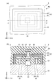
図1(a)は本実施形態に係る半導体装置を示す平面図であり、(b)は(a)に示すA−A’線による断面図である。
なお、各図は模式的なものであり、適宜誇張及び省略して描かれている。例えば、各構成要素は実際よりも少なく且つ大きく描かれている。また、図間において、構成要素の数及び寸法比等は、必ずしも一致していない。
図1(b)に示す破線の矢印は、水素の移動を模式的に表している。
本実施形態に係る半導体装置1を製造する際には、素子20、素子30、水素バリア部材40及び層間絶縁膜12等を形成した後に、高温の水素雰囲気に曝し、水素シンター処理を行う。このとき、水素イオン(H+)は層間絶縁膜12内を通過し、素子20に到達する。これにより、素子20において、シリコンとシリコン酸化物との界面に存在するダングリングボンドが水素によって終端される。この結果、素子20の信頼性が向上する。
図2(a)は素子20の具体例を示す断面図であり、(b)〜(d)は素子30の具体例を示す断面図である。
なお、素子20及び素子30の種類は、以下の具体例には限定されない。
次に、第2の実施形態について説明する。
図3(a)は本実施形態に係る半導体装置を示す平面図であり、(b)は(a)に示すB−B’線による断面図である。
本実施形態における上記以外の構成、動作及び効果は、前述の第1の実施形態と同様である。
次に、第3の実施形態について説明する。
図4(a)は本実施形態に係る半導体装置を示す平面図であり、(b)は(a)に示すC−C’線による断面図である。
本実施形態は、前述の第1の実施形態と第2の実施形態を組み合わせた例である。
本実施形態における上記以外の構成、動作及び効果は、前述の第1の実施形態と同様である。
次に、第4の実施形態について説明する。
本実施形態は、前述の第3の実施形態に係る半導体装置の製造方法である。
図5(a)〜(c)及び図6(a)〜(c)は、本実施形態に係る半導体装置の製造方法を示す断面図である。
本実施形態における上記以外の構成、動作及び効果は、前述の第3の実施形態と同様である。
10:半導体基板
12、12a、12b:層間絶縁膜
14:抵抗部材
20:素子
20a:MOSFET
21:コンタクト
22:配線
23:ビア
24:配線
25:STI
26:アクティブエリア
27:ソース・ドレイン領域
28:ゲート絶縁膜
29:ゲート電極
30:素子
30a:MOSFET
30b:メモリ素子
30c:抵抗素子
31:コンタクト
32:配線
33:ビア
34:配線
35:積層体
36:トンネル絶縁膜
37:浮遊ゲート電極
38:ブロック絶縁膜
39:制御ゲート電極
40:水素バリア部材
41:側壁
42:天板
43:下部
44:上部
50:水素バリア部材
60:水素バリア部材
61:側壁
62:箱状部材
63:下部
64:上部
65:側板
66:天板
71:レジスト膜
72:開口部
73:トレンチ
74:シリコン窒化部材
75:レジスト膜
R1、R2:領域
Claims (5)
- 半導体基板と、
前記半導体基板上に設けられた絶縁膜と、
少なくとも前記絶縁膜の下層部分に配置された第1素子と、
少なくとも前記絶縁膜の下層部分に配置された第2素子と、
前記半導体基板上に設けられ、前記絶縁膜の材料よりも水素が通過しにくい材料からなり、前記半導体基板と共に前記第2素子を囲み、前記第1素子を囲まない水素バリア部材と、
を備え、
前記絶縁膜はシリコン酸化物を含み、
前記水素バリア部材は、
金属からなり、上方から見て前記第2素子を囲む側壁と、
シリコン窒化物からなり、前記側壁に接した天板と、
を有した半導体装置。 - 前記水素バリア部材の形状は下面が開口した箱形であり、前記下面は前記半導体基板によって塞がれている請求項1記載の半導体装置。
- 半導体基板と、
前記半導体基板上に設けられた絶縁膜と、
少なくとも前記絶縁膜の下層部分に配置された第1素子と、
少なくとも前記絶縁膜の下層部分に配置された第2素子と、
前記半導体基板上に設けられ、前記絶縁膜の材料よりも水素が通過しにくい材料からなり、前記半導体基板と共に前記第2素子を囲み、前記第1素子を囲まない水素バリア部材と、
を備え、
前記絶縁膜はシリコン酸化物を含み、
前記水素バリア部材は、
金属からなり、上方から見て前記第2素子を囲む側壁と、
シリコン窒化物により一体的に形成され、前記第2素子及び前記側壁を囲む箱状部材と、
を有し、
前記側壁の上端は前記箱状部材に接した半導体装置。 - 前記第1素子はトランジスタである請求項1〜3のいずれか1つに記載の半導体装置。
- 前記第2素子は、トランジスタ、メモリ素子、又は、抵抗素子である請求項1〜4のいずれか1つに記載の半導体装置。
Priority Applications (2)
| Application Number | Priority Date | Filing Date | Title |
|---|---|---|---|
| JP2018050137A JP6878342B2 (ja) | 2018-03-16 | 2018-03-16 | 半導体装置 |
| US16/124,548 US10825771B2 (en) | 2018-03-16 | 2018-09-07 | Semiconductor device |
Applications Claiming Priority (1)
| Application Number | Priority Date | Filing Date | Title |
|---|---|---|---|
| JP2018050137A JP6878342B2 (ja) | 2018-03-16 | 2018-03-16 | 半導体装置 |
Publications (2)
| Publication Number | Publication Date |
|---|---|
| JP2019161192A JP2019161192A (ja) | 2019-09-19 |
| JP6878342B2 true JP6878342B2 (ja) | 2021-05-26 |
Family
ID=67904576
Family Applications (1)
| Application Number | Title | Priority Date | Filing Date |
|---|---|---|---|
| JP2018050137A Active JP6878342B2 (ja) | 2018-03-16 | 2018-03-16 | 半導体装置 |
Country Status (2)
| Country | Link |
|---|---|
| US (1) | US10825771B2 (ja) |
| JP (1) | JP6878342B2 (ja) |
Families Citing this family (1)
| Publication number | Priority date | Publication date | Assignee | Title |
|---|---|---|---|---|
| KR20230149150A (ko) | 2022-04-19 | 2023-10-26 | 삼성전자주식회사 | 반도체 메모리 소자 및 그의 제조 방법 |
Family Cites Families (6)
| Publication number | Priority date | Publication date | Assignee | Title |
|---|---|---|---|---|
| JPH09293869A (ja) | 1996-04-25 | 1997-11-11 | Nec Corp | 半導体装置およびその製造方法 |
| JP4181135B2 (ja) * | 2005-01-28 | 2008-11-12 | 株式会社東芝 | 半導体記憶装置 |
| JP2009016462A (ja) * | 2007-07-03 | 2009-01-22 | Renesas Technology Corp | 半導体装置およびその製造方法 |
| JP2009158704A (ja) * | 2007-12-26 | 2009-07-16 | Panasonic Corp | 半導体装置及びその製造方法 |
| JP2015109343A (ja) * | 2013-12-04 | 2015-06-11 | キヤノン株式会社 | 半導体装置の製造方法 |
| JP2016219550A (ja) | 2015-05-18 | 2016-12-22 | キヤノン株式会社 | 撮像装置、撮像システムおよび撮像装置の製造方法 |
-
2018
- 2018-03-16 JP JP2018050137A patent/JP6878342B2/ja active Active
- 2018-09-07 US US16/124,548 patent/US10825771B2/en active Active
Also Published As
| Publication number | Publication date |
|---|---|
| US10825771B2 (en) | 2020-11-03 |
| JP2019161192A (ja) | 2019-09-19 |
| US20190287917A1 (en) | 2019-09-19 |
Similar Documents
| Publication | Publication Date | Title |
|---|---|---|
| US20210249413A1 (en) | Semiconductor devices | |
| JP6947987B2 (ja) | 半導体集積回路装置 | |
| US10896956B2 (en) | Field effect transistor with reduced contact resistance | |
| US10804403B2 (en) | Method of fabricating semiconductor devices | |
| JP7077251B2 (ja) | 半導体装置 | |
| CN108122917B (zh) | 半导体器件 | |
| CN108962993B (zh) | 半导体装置及其制造方法 | |
| TW201813061A (zh) | 半導體裝置及其製造方法 | |
| CN108063157A (zh) | 半导体装置 | |
| JP2006013303A (ja) | 半導体装置及びその製造方法 | |
| KR20160010271A (ko) | 반도체 디바이스 및 수직 구조물을 형성하는 방법 | |
| KR20230053958A (ko) | 반도체 장치 | |
| JP7368107B2 (ja) | 半導体装置 | |
| CN102856207B (zh) | 一种半导体结构及其制造方法 | |
| CN107482047A (zh) | 半导体装置 | |
| US10978422B2 (en) | Vertical transistor device and method for fabricating the same | |
| JP6878342B2 (ja) | 半導体装置 | |
| CN105336726A (zh) | 半导体装置 | |
| CN110416292A (zh) | 包括栅极分离区的半导体器件 | |
| JP6889074B2 (ja) | 集積回路装置 | |
| TWI695477B (zh) | 半導體結構及其製作方法 | |
| JP5563811B2 (ja) | 半導体装置および半導体装置の製造方法 | |
| JP2007165780A (ja) | 半導体装置 | |
| CN100550424C (zh) | 半导体器件及其制造方法 | |
| CN116406227A (zh) | 包括电容器结构的半导体器件 |
Legal Events
| Date | Code | Title | Description |
|---|---|---|---|
| A621 | Written request for application examination |
Free format text: JAPANESE INTERMEDIATE CODE: A621 Effective date: 20200115 |
|
| A131 | Notification of reasons for refusal |
Free format text: JAPANESE INTERMEDIATE CODE: A131 Effective date: 20210129 |
|
| A977 | Report on retrieval |
Free format text: JAPANESE INTERMEDIATE CODE: A971007 Effective date: 20210129 |
|
| A521 | Request for written amendment filed |
Free format text: JAPANESE INTERMEDIATE CODE: A523 Effective date: 20210323 |
|
| TRDD | Decision of grant or rejection written | ||
| A01 | Written decision to grant a patent or to grant a registration (utility model) |
Free format text: JAPANESE INTERMEDIATE CODE: A01 Effective date: 20210406 |
|
| A61 | First payment of annual fees (during grant procedure) |
Free format text: JAPANESE INTERMEDIATE CODE: A61 Effective date: 20210428 |
|
| R150 | Certificate of patent or registration of utility model |
Ref document number: 6878342 Country of ref document: JP Free format text: JAPANESE INTERMEDIATE CODE: R150 |