JP6946776B2 - 回路基板 - Google Patents
回路基板 Download PDFInfo
- Publication number
- JP6946776B2 JP6946776B2 JP2017124666A JP2017124666A JP6946776B2 JP 6946776 B2 JP6946776 B2 JP 6946776B2 JP 2017124666 A JP2017124666 A JP 2017124666A JP 2017124666 A JP2017124666 A JP 2017124666A JP 6946776 B2 JP6946776 B2 JP 6946776B2
- Authority
- JP
- Japan
- Prior art keywords
- circuit board
- layer
- substrate
- board according
- via hole
- Prior art date
- Legal status (The legal status is an assumption and is not a legal conclusion. Google has not performed a legal analysis and makes no representation as to the accuracy of the status listed.)
- Active
Links
Images




Classifications
-
- H—ELECTRICITY
- H05—ELECTRIC TECHNIQUES NOT OTHERWISE PROVIDED FOR
- H05K—PRINTED CIRCUITS; CASINGS OR CONSTRUCTIONAL DETAILS OF ELECTRIC APPARATUS; MANUFACTURE OF ASSEMBLAGES OF ELECTRICAL COMPONENTS
- H05K1/00—Printed circuits
- H05K1/02—Details
- H05K1/0213—Electrical arrangements not otherwise provided for
- H05K1/0216—Reduction of cross-talk, noise or electromagnetic interference
- H05K1/0228—Compensation of cross-talk by a mutually correlated lay-out of printed circuit traces, e.g. for compensation of cross-talk in mounted connectors
-
- H—ELECTRICITY
- H05—ELECTRIC TECHNIQUES NOT OTHERWISE PROVIDED FOR
- H05K—PRINTED CIRCUITS; CASINGS OR CONSTRUCTIONAL DETAILS OF ELECTRIC APPARATUS; MANUFACTURE OF ASSEMBLAGES OF ELECTRICAL COMPONENTS
- H05K1/00—Printed circuits
- H05K1/02—Details
- H05K1/0213—Electrical arrangements not otherwise provided for
- H05K1/0216—Reduction of cross-talk, noise or electromagnetic interference
- H05K1/0218—Reduction of cross-talk, noise or electromagnetic interference by printed shielding conductors, ground planes or power plane
- H05K1/0219—Printed shielding conductors for shielding around or between signal conductors, e.g. coplanar or coaxial printed shielding conductors
-
- H—ELECTRICITY
- H05—ELECTRIC TECHNIQUES NOT OTHERWISE PROVIDED FOR
- H05K—PRINTED CIRCUITS; CASINGS OR CONSTRUCTIONAL DETAILS OF ELECTRIC APPARATUS; MANUFACTURE OF ASSEMBLAGES OF ELECTRICAL COMPONENTS
- H05K1/00—Printed circuits
- H05K1/02—Details
- H05K1/11—Printed elements for providing electric connections to or between printed circuits
- H05K1/115—Via connections; Lands around holes or via connections
-
- H—ELECTRICITY
- H05—ELECTRIC TECHNIQUES NOT OTHERWISE PROVIDED FOR
- H05K—PRINTED CIRCUITS; CASINGS OR CONSTRUCTIONAL DETAILS OF ELECTRIC APPARATUS; MANUFACTURE OF ASSEMBLAGES OF ELECTRICAL COMPONENTS
- H05K1/00—Printed circuits
- H05K1/18—Printed circuits structurally associated with non-printed electric components
- H05K1/181—Printed circuits structurally associated with non-printed electric components associated with surface mounted components
-
- H—ELECTRICITY
- H01—ELECTRIC ELEMENTS
- H01R—ELECTRICALLY-CONDUCTIVE CONNECTIONS; STRUCTURAL ASSOCIATIONS OF A PLURALITY OF MUTUALLY-INSULATED ELECTRICAL CONNECTING ELEMENTS; COUPLING DEVICES; CURRENT COLLECTORS
- H01R12/00—Structural associations of a plurality of mutually-insulated electrical connecting elements, specially adapted for printed circuits, e.g. printed circuit boards [PCB], flat or ribbon cables, or like generally planar structures, e.g. terminal strips, terminal blocks; Coupling devices specially adapted for printed circuits, flat or ribbon cables, or like generally planar structures; Terminals specially adapted for contact with, or insertion into, printed circuits, flat or ribbon cables, or like generally planar structures
- H01R12/70—Coupling devices
- H01R12/71—Coupling devices for rigid printing circuits or like structures
- H01R12/712—Coupling devices for rigid printing circuits or like structures co-operating with the surface of the printed circuit or with a coupling device exclusively provided on the surface of the printed circuit
- H01R12/716—Coupling device provided on the PCB
-
- H—ELECTRICITY
- H01—ELECTRIC ELEMENTS
- H01R—ELECTRICALLY-CONDUCTIVE CONNECTIONS; STRUCTURAL ASSOCIATIONS OF A PLURALITY OF MUTUALLY-INSULATED ELECTRICAL CONNECTING ELEMENTS; COUPLING DEVICES; CURRENT COLLECTORS
- H01R12/00—Structural associations of a plurality of mutually-insulated electrical connecting elements, specially adapted for printed circuits, e.g. printed circuit boards [PCB], flat or ribbon cables, or like generally planar structures, e.g. terminal strips, terminal blocks; Coupling devices specially adapted for printed circuits, flat or ribbon cables, or like generally planar structures; Terminals specially adapted for contact with, or insertion into, printed circuits, flat or ribbon cables, or like generally planar structures
- H01R12/70—Coupling devices
- H01R12/71—Coupling devices for rigid printing circuits or like structures
- H01R12/72—Coupling devices for rigid printing circuits or like structures coupling with the edge of the rigid printed circuits or like structures
- H01R12/722—Coupling devices for rigid printing circuits or like structures coupling with the edge of the rigid printed circuits or like structures coupling devices mounted on the edge of the printed circuits
-
- H—ELECTRICITY
- H05—ELECTRIC TECHNIQUES NOT OTHERWISE PROVIDED FOR
- H05K—PRINTED CIRCUITS; CASINGS OR CONSTRUCTIONAL DETAILS OF ELECTRIC APPARATUS; MANUFACTURE OF ASSEMBLAGES OF ELECTRICAL COMPONENTS
- H05K1/00—Printed circuits
- H05K1/02—Details
- H05K1/0213—Electrical arrangements not otherwise provided for
- H05K1/0237—High frequency adaptations
- H05K1/025—Impedance arrangements, e.g. impedance matching, reduction of parasitic impedance
-
- H—ELECTRICITY
- H05—ELECTRIC TECHNIQUES NOT OTHERWISE PROVIDED FOR
- H05K—PRINTED CIRCUITS; CASINGS OR CONSTRUCTIONAL DETAILS OF ELECTRIC APPARATUS; MANUFACTURE OF ASSEMBLAGES OF ELECTRICAL COMPONENTS
- H05K2201/00—Indexing scheme relating to printed circuits covered by H05K1/00
- H05K2201/09—Shape and layout
- H05K2201/09209—Shape and layout details of conductors
- H05K2201/095—Conductive through-holes or vias
- H05K2201/09609—Via grid, i.e. two-dimensional array of vias or holes in a single plane
-
- H—ELECTRICITY
- H05—ELECTRIC TECHNIQUES NOT OTHERWISE PROVIDED FOR
- H05K—PRINTED CIRCUITS; CASINGS OR CONSTRUCTIONAL DETAILS OF ELECTRIC APPARATUS; MANUFACTURE OF ASSEMBLAGES OF ELECTRICAL COMPONENTS
- H05K2201/00—Indexing scheme relating to printed circuits covered by H05K1/00
- H05K2201/10—Details of components or other objects attached to or integrated in a printed circuit board
- H05K2201/10007—Types of components
- H05K2201/10189—Non-printed connector
-
- H—ELECTRICITY
- H05—ELECTRIC TECHNIQUES NOT OTHERWISE PROVIDED FOR
- H05K—PRINTED CIRCUITS; CASINGS OR CONSTRUCTIONAL DETAILS OF ELECTRIC APPARATUS; MANUFACTURE OF ASSEMBLAGES OF ELECTRICAL COMPONENTS
- H05K2201/00—Indexing scheme relating to printed circuits covered by H05K1/00
- H05K2201/10—Details of components or other objects attached to or integrated in a printed circuit board
- H05K2201/10227—Other objects, e.g. metallic pieces
- H05K2201/10356—Cables
Landscapes
- Engineering & Computer Science (AREA)
- Microelectronics & Electronic Packaging (AREA)
- Physics & Mathematics (AREA)
- Electromagnetism (AREA)
- Structure Of Printed Boards (AREA)
- Production Of Multi-Layered Print Wiring Board (AREA)
Description
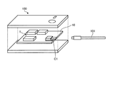
本実施の形態にかかる回路基板は、多層構造のプリント配線基板である。本実施の形態において、複数の層が形成されている積層体の部分を基体と呼ぶ。基体は、ビルドアップ工法により形成したものや、貫通多層板などが使用される。当該回路基板は、信号を伝送するハーネスを接続するためのコネクタを有し、コネクタと回路基板とは基体の取り付け穴(固定穴)でねじ等により締結されている。
中央領域1bの回路面の集積密度を、内層配線の厚みをより厚くして配線幅を狭めることにより高くし、高集積化した中央領域1bの空いた領域を縁1a若しくはその一部として利用しても良い。
実施の形態では、ビアホール12と取り付け穴11との位置が取り付け穴11がビアホール12の列の内側(中央領域1b側)になる配置のものについて一例を示した。この配置は、逆つまり取り付け穴11がビアホール12の列の外側(縁1a側)になる配置であっても良い。
1a 縁
1b 中央領域
10 基体
11 取り付け穴
12 ビアホール
13 メッキ層
C1 コネクタ
L1〜L8 第1層〜第8層
N1〜N8 GNDベタパターン
P1〜P7 誘電体層
Claims (10)
- 多層構造の基体を有する回路基板であって、
前記基体は、
信号を伝送するハーネスを接続するコネクタの固定穴と、
複数の層に設けられたGNDベタパターンと、
前記複数の層に設けられた各GNDベタパターンを電気的に接続するビアホールと、
を有し、
前記複数の層のうちの電源層の各厚みがより厚く、
前記電源層に接する誘電体層の各厚みが前記電源層に接しない各誘電体層よりも薄い、
ことを特徴とする回路基板。 - 前記GNDベタパターンは、前記基体の各層が有する、
請求項1に記載の回路基板。 - 前記固定穴に固定された前記コネクタの配置領域と該配置領域の近傍とにおいて各層に前記GNDベタパターンが設けられている、
請求項2に記載の回路基板。 - 前記ビアホールは、前記コネクタの前記配置領域の前記近傍に設けられている、
請求項3に記載の回路基板。 - 前記ビアホールは、前記基体の縁に設けられている、
請求項4に記載の回路基板。 - 前記ビアホールは、2列で設けられている、
請求項5に記載の回路基板。 - 前記ビアホールは、前記基体の外周に沿って2列で設けられている、
請求項6に記載の回路基板。 - 前記ビアホールは互いが重ならないように10mm以下の間隔で設けられている、
請求項7に記載の回路基板。 - 前記基体の内層配線は、厚みを厚くすることにより配線幅が狭められている、
請求項1乃至8の内の何れか一項に記載の回路基板。 - 前記ビアホールは、前記基体を貫通する貫通構造を有する、
請求項1乃至8の内の何れか一項に記載の回路基板。
Priority Applications (2)
| Application Number | Priority Date | Filing Date | Title |
|---|---|---|---|
| JP2017124666A JP6946776B2 (ja) | 2017-06-26 | 2017-06-26 | 回路基板 |
| US16/009,397 US10687414B2 (en) | 2017-06-26 | 2018-06-15 | Circuit board |
Applications Claiming Priority (1)
| Application Number | Priority Date | Filing Date | Title |
|---|---|---|---|
| JP2017124666A JP6946776B2 (ja) | 2017-06-26 | 2017-06-26 | 回路基板 |
Publications (2)
| Publication Number | Publication Date |
|---|---|
| JP2019009322A JP2019009322A (ja) | 2019-01-17 |
| JP6946776B2 true JP6946776B2 (ja) | 2021-10-06 |
Family
ID=64692998
Family Applications (1)
| Application Number | Title | Priority Date | Filing Date |
|---|---|---|---|
| JP2017124666A Active JP6946776B2 (ja) | 2017-06-26 | 2017-06-26 | 回路基板 |
Country Status (2)
| Country | Link |
|---|---|
| US (1) | US10687414B2 (ja) |
| JP (1) | JP6946776B2 (ja) |
Families Citing this family (6)
| Publication number | Priority date | Publication date | Assignee | Title |
|---|---|---|---|---|
| JP2020021808A (ja) * | 2018-07-31 | 2020-02-06 | キヤノン株式会社 | 回路基板とその回路基板を有する電子装置 |
| JP7547036B2 (ja) * | 2019-08-09 | 2024-09-09 | キヤノン株式会社 | プリント基板 |
| KR20210031303A (ko) * | 2019-09-11 | 2021-03-19 | 삼성전자주식회사 | 회로 기판에 실장되는 커넥터를 포함하는 전자 장치 |
| CN115441264A (zh) * | 2021-06-05 | 2022-12-06 | 富士康(昆山)电脑接插件有限公司 | 端子模组及具有该端子模组的电连接器 |
| US12347978B2 (en) * | 2022-07-18 | 2025-07-01 | Raytheon Company | Overmold-overmold micro radio frequency connector |
| WO2025211998A1 (en) * | 2024-04-04 | 2025-10-09 | Magna Electronics Sweden Ab | Enhanced pcb and pcb housing |
Family Cites Families (21)
| Publication number | Priority date | Publication date | Assignee | Title |
|---|---|---|---|---|
| JPH1154944A (ja) * | 1997-08-07 | 1999-02-26 | Toshiba Corp | 回路基板 |
| JP2000286587A (ja) * | 1999-03-30 | 2000-10-13 | Matsushita Electric Ind Co Ltd | 外部ケーブル接続用コネクタ部の電磁シールド構造 |
| JP2001007456A (ja) * | 1999-06-17 | 2001-01-12 | Toshiba Corp | 配線回路基板 |
| JP2001251063A (ja) | 2000-03-06 | 2001-09-14 | Matsushita Electric Ind Co Ltd | 回路基板およびこれを用いたテレビジョン受信機 |
| JP2002222892A (ja) * | 2001-01-26 | 2002-08-09 | Kyocera Corp | 多層配線基板 |
| JP2004055988A (ja) | 2002-07-23 | 2004-02-19 | Fujitsu Ltd | 情報処理装置 |
| JP3960178B2 (ja) * | 2002-09-17 | 2007-08-15 | 株式会社デンソー | 多層プリント基板 |
| CN100344976C (zh) * | 2002-10-31 | 2007-10-24 | 株式会社爱德万测试 | 被测量组件搭载板、探针卡以及组件接口部 |
| DE102004016146B4 (de) * | 2004-04-01 | 2006-09-14 | Epcos Ag | Elektrisches Vielschichtbauelement |
| JP4551730B2 (ja) * | 2004-10-15 | 2010-09-29 | イビデン株式会社 | 多層コア基板及びその製造方法 |
| US7355125B2 (en) * | 2005-11-17 | 2008-04-08 | International Business Machines Corporation | Printed circuit board and chip module |
| JP5070077B2 (ja) | 2008-02-08 | 2012-11-07 | 株式会社リコー | Lsiを装備する電装基板,画像形成制御板および画像形成装置 |
| WO2010114825A1 (en) * | 2009-03-30 | 2010-10-07 | Magna Mirrors Of America, Inc. | Electro-optic rearview mirror assembly for vehicle |
| KR101072591B1 (ko) | 2009-08-10 | 2011-10-11 | 삼성전기주식회사 | Emi 노이즈 저감 인쇄회로기판 |
| US8319116B2 (en) * | 2009-09-11 | 2012-11-27 | Oracle America, Inc. | Rib reinforcement of plated thru-holes |
| US8371316B2 (en) * | 2009-12-03 | 2013-02-12 | International Test Solutions, Inc. | Apparatuses, device, and methods for cleaning tester interface contact elements and support hardware |
| JP2012094843A (ja) * | 2010-09-30 | 2012-05-17 | Incorporated Educational Institution Meisei | 回路基板、電源構造体、回路基板の製造方法、および電源構造体の製造方法 |
| DE102011077206B4 (de) * | 2011-06-08 | 2019-01-31 | Zf Friedrichshafen Ag | Leiterplatte und Steuergerät für ein Getriebe eines Fahrzeugs mit der Leiterplatte |
| CN102496804A (zh) * | 2011-11-22 | 2012-06-13 | 华为终端有限公司 | Usb连接器及电子设备 |
| US8834182B2 (en) * | 2012-10-17 | 2014-09-16 | Microelectronics Assembly Technologies | Pierced flexible circuit and compression joint |
| DE102013211640A1 (de) * | 2013-06-20 | 2014-12-24 | Osram Opto Semiconductors Gmbh | Optoelektronische Anordnung |
-
2017
- 2017-06-26 JP JP2017124666A patent/JP6946776B2/ja active Active
-
2018
- 2018-06-15 US US16/009,397 patent/US10687414B2/en active Active
Also Published As
| Publication number | Publication date |
|---|---|
| US20180376581A1 (en) | 2018-12-27 |
| US10687414B2 (en) | 2020-06-16 |
| JP2019009322A (ja) | 2019-01-17 |
Similar Documents
| Publication | Publication Date | Title |
|---|---|---|
| JP6946776B2 (ja) | 回路基板 | |
| US10741303B2 (en) | Transmission line, flat cable, and electronic device | |
| US6236572B1 (en) | Controlled impedance bus and method for a computer system | |
| US8309863B2 (en) | Printed wiring board | |
| US7435912B1 (en) | Tailoring via impedance on a circuit board | |
| EP2654387B1 (en) | Printed circuit board | |
| EP1945010B1 (en) | Multi-layer substrate and electronic device having the same | |
| JP5983780B2 (ja) | プリント配線基板、電子機器及び配線接続方法 | |
| KR20170048575A (ko) | 프린트 배선판 | |
| CN104040787A (zh) | 具有降低的串扰的印刷电路板 | |
| CN109587942B (zh) | 用于反钻式差分通孔的间隙大小减小 | |
| US7086869B1 (en) | Flexible cable interconnect with integrated EMC shielding | |
| WO2008003021A2 (en) | Shielded via | |
| KR102447839B1 (ko) | 회로 기판 및 이를 포함하는 전자 기기 | |
| KR101888592B1 (ko) | 연성회로기판 및 그 제조방법 | |
| KR100666224B1 (ko) | 개구를 가지는 리지드 플렉시블 인쇄회로기판 | |
| US7186924B2 (en) | Dielectric structure for printed circuit board traces | |
| US10128810B2 (en) | Impedance matching structure of transmission line | |
| US7679005B2 (en) | Circuitized substrate with shielded signal lines and plated-thru-holes and method of making same, and electrical assembly and information handling system utilizing same | |
| US20030085055A1 (en) | Substrate design and process for reducing electromagnetic emission | |
| US20080165514A1 (en) | Printed circuit board | |
| US10729003B2 (en) | Anti-electromagnetic interference circuit board | |
| JP2013222924A (ja) | 部品内蔵基板 | |
| US8664537B2 (en) | Method and apparatus for reducing signal noise | |
| US20070181996A1 (en) | Circuit board |
Legal Events
| Date | Code | Title | Description |
|---|---|---|---|
| A621 | Written request for application examination |
Free format text: JAPANESE INTERMEDIATE CODE: A621 Effective date: 20200226 |
|
| A977 | Report on retrieval |
Free format text: JAPANESE INTERMEDIATE CODE: A971007 Effective date: 20201224 |
|
| A131 | Notification of reasons for refusal |
Free format text: JAPANESE INTERMEDIATE CODE: A131 Effective date: 20210105 |
|
| A521 | Request for written amendment filed |
Free format text: JAPANESE INTERMEDIATE CODE: A523 Effective date: 20210303 |
|
| TRDD | Decision of grant or rejection written | ||
| A01 | Written decision to grant a patent or to grant a registration (utility model) |
Free format text: JAPANESE INTERMEDIATE CODE: A01 Effective date: 20210817 |
|
| A61 | First payment of annual fees (during grant procedure) |
Free format text: JAPANESE INTERMEDIATE CODE: A61 Effective date: 20210830 |
|
| R151 | Written notification of patent or utility model registration |
Ref document number: 6946776 Country of ref document: JP Free format text: JAPANESE INTERMEDIATE CODE: R151 |